Note: Descriptions are shown in the official language in which they were submitted.
CA 02127442 1999-09-17
- 1 -
IMAGE DISPLAY
The present invention relates to a flat-type
image display apparatus. More particularly, it relates to
an improved image display apparatus with less luminance
unevenness.
Figs. 16 and 17 are, respectively, an exploded
perspective view of a conventional flat-type image display
apparatus as disclosed in, for example, Japanese
Unexamined Patent Publications Nos. 2 2 6 9 4 9 / 19 9 l and
18 4 2 3 9 / 19 8 8 and an enlarged, partially broken away view of
a principal part of another example. In Figs. 16 and 17,
numeral 1 denotes string like hot cathodes each of which
is connected to a support and emits electrons when
energized, and numeral 3 denotes perforated cover
electrodes each covering each string like hot cathode 1
and each shaped elliptic in section. Each cover electrode
3 has small apertures permitting electrons to pass
therethrough and serves to lead electrons out of the
corresponding string like hot cathode 1 when applied with
an appropriate potential. An electron-emitting source 40
comprises the string like hot cathodes 1, perforated cover
electrodes 3 and back electrodes 42 fixing the cover
electrodes 3 arranged in parallel and each assuming a
3 0 potential equal to that of the corresponding cover
electrode 3. Numeral 8 denotes a front glass which is
coated on the inner surface thereof with three types of
luminous elements (not shown) in a dotted or striped
manner and with an aluminum film (not shown) covering
these luminous elements for electric conduction, the
luminous elements being adapted to be excited by electrons
emitted from the electron-emitting source 40 to emit light
in respective colors, i.e., red, green and blue.
~.~~'~4~~
- 2 -
In such a configuration, an application of a
voltage of about 5 to about 30 kV to the aluminum film of
the front glass 8 causes electrons to accelerate and
thereby the luminous elements (not shown) to be excited to
emit light. Numeral 4 denotes a control electrode for
permitting or shutting off the passage of electrons led
out by each cover electrode 3 toward the front glass 8,
the control electrode being interposed between the front
glass 8 and the string like hot cathodes 1. Numeral 10
denotes a focusing electrode to be applied with a
predetermined voltage for causing electron beam having
passed through an electron-pass aperture 4a of the control
electrode 4 to pass through an electron-pass aperture l0a
and to be focused upon the corresponding dot of luminous
element. The control electrode 4 includes a surface-
insulative substrate 5 having electron-pass apertures 4a
corresponding to pixels formed on the front glass 8, for
example, a surface-insulative substrate 5 formed by
coating an etch-perforated metallic substrate with an
insulating film, a first control electrode group 6A
including metallic electrodes 6 which are patterned like
stripes having electron-pass apertures and arranged on the
lower side of the surface-insulative substrate 5, or on
the electron-emitting source 40 side, corresponding to
respective columns of pixels, and a second control
electrode group 7A, similar to the former group, including
metallic electrodes 7 which are patterned like stripes
having electron-pass apertures and arranged on the upper
side of the surface-insulative substrate 5 corresponding
to respective rows of pixels. Each metallic electrode of r
the first and second control electrode groups 6A and 7A is
formed of, for example, a nickel film. The first and
second control electrode groups 6A and 7A are insulated
from each other by a nickel-free portion existing within
each electron-pass aperture though nickel penetrates
thereinto from both sides. The first control electrode
group 6A further includes isolation grooves 44, or
nickel-free insulating grooves, which extend between
- 3 -
adjacent electron-pass apertures 4a in the direction
perpendicular to the string like hot cathode 1.
Similarly, the second control electrode group 7A includes
isolation grooves 45 extending in the direction
perpendicular to the isolation grooves 44 of the first
control electrode group 6A. These are disposed within a
sealed enclosure in the form of flat panel, the inside of
which is kept vacuum. Each of the electrodes is usually
disposed in a flattened manner by means of a fix-hold
member (not shown) and electrically connected to the
outside through a seal portion provided on a lateral
surface of the sealed enclosure.
Figs. 18 and 19 also illustrate another
conventional flat-type image display apparatus. Fig.
19(a) is a perspective view of the arrangement of control
electrodes 4 shown in Fig. 18, and Fig. 19 (b) is an
enlarged view of a portion thereof. In Figs. 18 and 19,
same numerals are used to denote corresponding parts of
Figs 16 and 17, and the descriptions on such parts are
omitted. This example has front glass 8 shaped as curved
and is so structured as to allow stress relaxation (to be
described later) to be encouraged and the overall
apparatus to be lightened. Further, this example has
first control electrode group 6A and second control
electrode group 7A which comprise stripe-like metallic
electrodes 6 and stripe-like metallic electrodes 7,
respectively, instead of the metallic film penetrating
into electron-pass apertures of insulating substrate 5.
These electrodes 6 and 7 are bonded to the insulating
substrate 5 in such a manner that their electron-pass
apertures are coincident with the corresponding
electrode-pass apertures of the insulating substrate 5
thereby defining electron-pass apertures 4a of the control
electrodes 4.
Description on the operation is as follows:
Thermoelectrons emitted from the string like hot
cathode 1 are led out by a positive potential of about 5
to about 40 V applied to the perforated cover electrode 3,
, .:s
:
f . .
.
h
~ y
r "
. . ...:
i
i~ .
~~~ . . y,
~ ,'.
~'.
,
,
' . ; r ;
~.
. , .,
. . ,
A . .
.
.
..' , . .s ,
. ;'.. ,.
. .
.. '
" . . .
' .
.; ..
. ~ . .,;.
'
,..
,.. .. ,,.. ,
~~
, ~
.
;.
,; ...
' ,
N
- 4 -
the positive potential being relative to the average
potential of the string like hot cathode 1 assumed as a
reference potential (hereinafter this average potential
will be assumed to be 0 V). Further, by applying a
positive potential of about 20 V to about 100 V relative
to the potential of string like hot cathode 1 to one
electrode of the first control electrode group 6A
comprising metallic electrodes 6 arranged in the direction
perpendicular to the string like hot cathode 1, the
thermoelectons are drawn toward this electrode and reaches
the control electrode 4. This apparatus is designed such
that the density of an electron beam on the surface of any
metallic electrode of the first control electrode group 6A
is made substantially uniform by adjusting the elliptic
shape of the perforated cover electrode 3, the position of
the first control electrode group 6A and the voltage to be
applied to each metallic electrode 6.
It should be noted that although the operation
of this control electrode 4 is not described in Japanese
Unexamined Patent Publication No. 184239/1988, it is
similar to the operation of typical matrix-type displays
as disclosed in, for example, Japanese Unexamined Patent
Publication Nos. 172642/1987, 126688/1989 and
226949/1991.
If only one metallic electrode 6 of the first
control electrode group 6A assumes a positive potential
(on-state) while the others assume 0 V or negative
potential (off-state), the electrons emitted from the
string like hot cathode 1 are attracted only by that
control electrode 6 at a positive potential and enter each '
electrode-pass aperture 4a of this control electrode 6.
However, not all the electrons entering the aperture pass
therethrough toward the front glass 8. When the second
control electrode group 7A is made to assume 0 V or
negative potential, a negative potential region is
produced by the second control electrode group 7A, so that
the electrons stop within the electron-pass aperture 4a.
Consequently, electrons are allowed. to pass
~~~'~~4~
- 5 -
through only the electron-pass aperture 4a lying at the
intersection of the metallic electrode, being applied with
a positive potential, of the first control electrode group
6A and the metallic electrode, being applied with a
positive potential (for example 40 V to 100 V), of the
second control electrode group 7A. The electrons having
passed through the aperture 4a cause the luminous element
positioned coincident with the aperture 4a to emit light.
Therefore, desired pixel display can be achieved by
controlling the application of voltage to metallic
electrodes 6 and 7 so that the intersection thereof is
located corresponding to a desired position.
The luminance of each pixel is controlled by
adjusting the on-state duration of each electrode of the
second control electrode group 7A.
In this case, electron beam 2 (refer to Fig. 18)
passing through the electron-pass aperture 4a is required
to be focused within a phosphor dot corresponding to the
aperture 4a. If the electron beam 2 passing dot of a
luminous element through the electron-pass aperture 4a is
incident on another too, color fringing will occur in the
resulting image, or unclear contour of the image will
result. For that reason, the focusing electrode 10 is
provided for the purpose of controlling the path of the
electron beam so that the electron beam is incident within
a desired dot of a luminous element by applying an
appropriate voltage to the, focusing electrode.
Flat-type image display apparatus utilizing
electrom beam need to have electron-passing areas all kept
vacuum and hence requires a sealed vacuum enclosure.
Where an image display apparatus is sold as an practical
commercial article, for example, a television set for
domestic use, it is desirable that the vacuum enclosure be
made as light and thin (or small in the length in the
direction perpendicular to the screen) as possible.
Where the above-mentioned conventional flat-type
image display apparatus have a screen size as small as
about 16 in., the glass thickness of the sealed enclosure
~"~2'~~~~
- 6 -
does not need to be made so thick. However, where the
screen size is as large as 20 in. or greater, the glass
thickness needs to be made not smaller than about 20 mm to
provide the enclosure with a sufficient strength against
vacuum. This results in a difficulty in lightening
display apparatus of this type.
The most effective approach to lighten the
vacuum enclosure is to shape the enclosure into a sphere
ensuring the least stress concentration. However, this is
against the demand mentioned above for a thinner
enclosure. Assuming that the vacuum enclosure of a
flat-type display apparatus is a box-like vacuum enclosure
11, as shown in section at Fig. 20(a), for accommodating
an image display unit Ila, stress concentration caused by
the pressure difference between the inside and outside of
the vaccum enclosure 11 will occur at angular portions and
central portions of the screen indicated by arrow. If a
reinforcing member is added to the enclosure at the
angular portions or like portions to withstand such
stress, the weight of the enclosure increases
significantly. Therefore, the vacuum enclosure 11 in the
form of oval in section as shown in Fig. 20(b) is most
easily realized with the aim of making the enclosure 11
light and thin.
Typically, the phosphor for use in a television
set is coated directly on the inner surface of the
front glass forming part of the vacuum enclosure. This is
because the provision of another glass plate or the like
intermediate the front glass and the luminous element
would cause light to reduce and hence the luminance of the '
display screen to decrease, because the screen would
provide unclear image even though the space between the
front glass and the glass plate coated with the luminous
element is made vacuum, because the manufacturing cost is
low, and like reasons.
In consequence, it is appreciated that the front
glass of the vacuum enclosure needs to be shaped curved as
having a curvature as shown in Fig. 18 so as to have a
~1~'~~~~
_~_
lightened weight and a reduced thickness, and that the
luminous element is desirably coated on the inner surface
of the front glass.
In the structure shown in Fig. 18, however,
since the control electrode 4 and focusing electrode 10
are flat though the front glass is curved, there is a
difference in the distance from the control electrode 4 or
focusing electrode 10 to the front glass coated with the
luminous element between end portion and central portion
of the screen.
As described above, the focusing electrode 10 is
applied with a desired voltage to focus electron beam 2
within a desired dot of luminous element. However, as
shown in the enlarged sectional view at Fig. 21, where
there is only one focusing electrode 10 and the voltage
capable of being applied is fixed, the beam diameter
reaches the minimum (becomes just focused) at only one
point P,,. Accordingly, where the distance Daf between
the focusing electrode 10 and the front glass 8 provided
with the aluminum film serving as the anode on the inner
side thereof is uneven, it is impossible to cause the
electron beam 2 to assume a minimum beam diameter at
overall surface of the front glass 8. Stated otherwise,
the beam diameter of electron beam 2 on the front glass is
not fixed at different locations on the screen of the
front glass 8 and, hence, the electron beam 2 becomes
" fuzzy" at point PZ as shown in Fig. 18.
Where the electron beam 2 becomes " fuzzy", for
example, the beam diameter of electron beam 2a exceeds the
size of a pixel as shown in Fig. 22, black matrix 12 is '
also irradiated with the electron beam 2a, so that the
intensity of the beam to be applied onto luminous element
9 decreases and, hence, the luminous intensity of the
corresponding pixel decreases. Therefore, when the
overall screen is viewed, luminance unevenness occurs.
Alternatively, where the electron beam 2 is an electron
beam 2a having a beam diameter such that the beam extends
from the subject pixel to pixels adjacent thereto over the
212'~~42
pitch therebetween, the pixels other than desired to emit
light are also caused to emit light, so that phenomena are
developed such as color fringing and blurred contour of
the resulting image.
Accordingly, when point PZ at which the electron
beam 2 becomes " fuzzy" appears in a portion of the
screen, luminance unevenness, color fringing or the like
occurs at point P2. This is a fatal defect to a
commercial article having a display screen.
To overcome such problem, there is disclosed in,
for example, Japanese Unexamined Patent Publication No.
19947/1992 a structure wherein the wall of a sealed vaccum
enclosure on light-emitting means side, the light-emitting
means (phosphor-coated surface), an electron beam control
electrode and an electron beam lead-out electrode are
curved as having respective curvatures substantially equal
to each other, while in addition a correction means is
provided to render the quantity of electron beam incident
on the electron beam lead-out electrode uniform in the
horizontal direction; or a structure wherein the wall of
the sealed vacuum enclosure on the light-emitting means
side, a string like hot cathode, the electron beam lead-
out electrode, electron beam control electrode and the
light-emitting means are shaped into curved lines or
curved surfaces as having respective curvatures
substantially equal to each other. In this structure,
however, the electron beam lead-out electrode cannot be
applied to an electrode (perforated cover electrode)
shaped elliptic in section and adapted to cover each
string like hot cathode since the electron beam lead-out '
electrode is in the form of one plate and is a common
electrode for all the string like hot cathodes, for
avoiding the occurrence of substantial deformation
thereof even though it is curved. In more detail, each
perforated cover electrode needs to have a curvature small
enough to form an elliptic section and further another
curvature harmonizing with the curved surface of the front
glass. In addition, the perforated cover electrode is
CA 02127442 1999-09-17
' - 9 -
located very near the string like hot cathode and hence is
heated thereby to elevated temperatures, leading to severe
thermal deformation. As a result, there arise problems that
the luminance distribution on the display screen is possible
to be extremely degraded, insulation failure between the
perforated cover electrode and the cathode becomes likely,
the life time of the cathode is shortened, and the like.
An object of the present invention is to provide a
highly reliable image display apparatus which is lightened
and thinned by employing a sealed vacuum enclosure
comprising a curved surface and is capable of displaying a
clear image free of luminance unevenness over the entire
screen and of being manufactured with less cost.
The present invention relates to an image display
apparatus comprising: a cathode for emitting electrons; a
perforated cover electrode for leading out and accelerating
the electrons emitted from the cathode; a control electrode
disposed in substantially parallel with the cathode and
having an electron-pass aperture permitting the emitted
electrons to pass therethrough, the control electrode being
adapted to control an electron beam passing through the
electron-pass aperture; a luminous element which emits light
when irradiated with the emitted electrons and is formed on
a curved screen panel; and a focusing electrode disposed
between the control electrode and the luminous element and
having an electron-pass aperture and a means for correcting
the beam diameter of the electron beam on the luminous
element which varies in accordance with a variation in the
distance between the luminous element and the control
electrode. The correcting means creates at least two kinds
of the electron beams having different focal points from the
focusing electrode.
The aforesaid means for correcting the beam diameter of
the electron beam on the luminous element can be realized by
dividing the focusing electrode into a plurality of
CA 02127442 1999-09-17
- 10 -
electrodes and applying different voltages to respective
electrodes.
Another aspect of the present invention relates to an
image display apparatus comprising a cathode for emitting
electrons, a perforated cover electrode for leading out and
accelerating the electrons emitted from the cathode, and a
control electrode disposed substantially parallel with the
cathode and having an electron-pass aperture permitting the
emitted electrons to pass therethrough. The control
electrode is adapted to control an electron beam passing
through the electron-pass aperture. A luminous element,
which emits light when irradiated with the emitted
electrons, is formed on a curved screen panel. A focusing
electrode is disposed between the control electrode and the
luminous element. The focusing electrode is disposed such
that the ratio of the distance between the focusing
electrode and the control electrode to that between the
focusing electrode and the luminous element is substantially
constant over an entire display screen.
The present invention also relates to an image display
apparatus comprising a cathode for emitting electrons, a
perforated cover electrode for leading out and accelerating
the electrons emitted from the cathode, and a control
electrode disposed substantially parallel with the cathode
and having an electron-pass aperture permitting the emitted
electrons to pass therethrough. The control electrode is
adapted to control an electron beam passing through the
electron-pass aperture. A luminous element, which emits
light when irradiated with the emitted electrons, is formed
on a curved screen panel. A focusing electrode is disposed
between the control electrode and the luminous element and
has an electron-pass aperture and a means for correcting the
beam diameter of the electron beam on the luminous element.
The correcting means comprises the electron-pass aperture of
the focusing electrode having a size of the electron-pass
CA 02127442 1999-09-17
~ - l0a -
aperture which is varied in accordance with the distance
between the focusing electrode and the luminous element.
Another aspect of the present invention relates to an
image display apparatus comprising a cathode for emitting
electrons, a perforated cover electrode for leading out and
accelerating the electrons emitted from the cathode, and a
control electrode disposed substantially parallel with the
cathode and having an electron-pass aperture permitting the
emitted electrons to pass therethrough. The control
electrode is adapted to control an electron beam passing
through the electron-pass aperture. A luminous element
emits light when irradiated with the emitted electrons. A
focusing electrode is disposed between the control electrode
and the luminous element. The focusing electrode is divided
into at least two electrodes, each of the at least two
electrodes being independently controlled. The focusing
electrode includes a plurality of electron-pass apertures
through which the electron beam passes.
The present invention also relates to an image display
apparatus comprising: a cathode for emitting electrons; a
perforated cover electrode for leading out and accelerating
the electrons emitted from the cathode; a control electrode
disposed substantially parallel with the cathode and having
an electron-pass aperture permitting the emitted electrons
to pass therethrough and adapted to control an electron beam
passing through the electron-pass aperture; a luminous
element which emits light when irradiated with the emitted
electrons; a focusing electrode disposed between the control
electrode and the luminous element and having an electron-
pass aperture permitting the emitted electrons to pass
therethrough; and a second grid disposed between the control
electrode and the perforated electrode and having an
electrode-pass aperture for correcting the brightness of the
luminous element which varies in accordance with a variation
CA 02127442 1999-09-17
- lOb -
in the distance between the luminous element and the
perforated cover electrode; the luminous element, the
focusing electrode and the control electrode comprising
respective curved surfaces having a substantially equal
curvature, the perforated cover electrode and the cathode
respectively comprising a plurality of perforated cover
electrodes and a plurality of cathodes, the perforated cover
electrodes and the cathodes being arranged in an array on a
curved surface having a curvature substantially larger than
the former curvature or on a flat plane.
The term "a substantially equal curvature" is herein
meant to express such an extent that the respective
distances between the luminous element and individual
electrodes are almost equal to each other and, hence, a
30
- 11 -
problem of luminance unevenness due to a variation in the
beam diameter of the electron beam on the luminous element
will not occur.
The aforesaid second grid may comprise a curved
surface having a curvature larger than or substantially
equal to that of the control electrode or a flat plane.
To improve the uniformity ratio of electron
beam, preferably, the perforated cover electrodes and the
cathodes may be arranged with increasing pitch as viewed
in the direction from a central portion to a peripheral
portion; the curved surface or flat plane on which the
perforated cover electrodes and the cathodes are formed
may be spaced apart from the second grid by a distance 1.0
to 6.0 times as large as the pitch at which the cathodes
are arranged in array; the rate of hole area of at least
one of the second grid and the perforated cover electrode
may be made large in a central portion and made small in a
peripheral portion when viewed in the arrangement pitch
direction of the perforated cover electrodes and cathodes;
the perforated cover electrode and the cathode may be
disposed such that the distance therebetween is made small
in the central portion and made large in the peripheral
portion when viewed in the arrangement pitch direction of
the perforated cover electrodes and cathodes; or the
second grid may be divided into at least three sections
in such arrangement pitch direction so that the central
section of the second grid is applied with a large voltage
and the peripheral sections thereof with a small voltage.
According to the present invention, for example,
the focusing electrode is dividedly formed, and ' each
divided electrode can be applied with a voltage inversely
proportional to the distance by which it is spaced apart
from the luminous element serving as the anode.
Accordingly, it is possible to make the beam diameter of
an electron beam on the display screen substantially
uniform and small over the entire screen and hence to
display a clear image over the entire screen.
Further, according to the present invention, the
rr
~
, ..
' '
, ,'
.
'
'
' . : ~ . , .
... ~
~..~ , , y, . .. . ' .
f,'. ~ ~ .., . . . .., , .., . . ,: ". ~ .. , ~. . ' . . ~ '. ~
, ' ~ _ 1
~I ..
~ ,
~ ~
'
~'
~~
..
! ' ' ,' , ., , ,.
, ' ; ' , ".
J ~. ,. ..
'.
.
. .
-:. ,.
f ..... : .... : ~ ~ . ~
,
~' . . . 7
'.
"
~
~
.
., . . , ,
Y: '~ '. . .. .. ,
.; .,~. .' . .. .. ,
. . .,
,,~, t ;
"
,...
; ..
.1 . . . ~~ ' ' ~~ .. . ~
~
~ . :
:'
'
. . ,
...~ ,
, .
' ,..,
~ ' ..
' .
' ;.'.. .
, . . . ~. ..,
.. , .. ... ,:... ~ ... . . , ..-." ,.' ; . ' ~'.
. . ,. .
., :.. ... i.'.. '. . .
S
CA 02127442 1999-09-17
- 12 -
curvature of each of the focusing electrode and control
electrode is made substantially equal to that of the curved
surface of the luminous element, while the second grid is
provided between the control electrode and the perforated
cover electrode. Such arrangement allows the second grid to
correct the location at which electron beam assumes its
minimum beam diameter, whereby the uniformity ratio of
electron beam incident on the control electrode can be made
constant even though the distance between the perforated cover
electrode and the control electrode varies. This assures
display of clear image with little luminance unevenness over
the entire screen.
Furthermore, since the surface of the luminous element,
i.e., the wall of the vacuum enclosure is curved, stress
concentration can be avoided, and the vacuum enclosure can be
lightened and thinned. In addition, since each electrode can
be made planar, it is possible to minimize the manufacturing
costs.
The invention will be described in greater detail with
reference to the accompanying drawings.
Fig. 1 is an exploded perspective view of a principal
part of one example of an image display apparatus according to
the present invention for illustrating the arrangement
thereof.
Fig. 2 is a graphic representation showing characteristic
curves representing the relation between the distance between
the front glass and the focusing electrode and the focusing
electrode voltage needed to decrease the beam diameter of
electron beam on the front glass.
Fig. 3 is a perspective view illustrating an example of
the focusing electrode of divided structure.
Fig. 4 is an explanatory view for illustrating an example
of the way of applying voltage to the focusing electrode.
Fig. 5 is a sectional view of an example of a structure
for varying the distance between the focusing electrode and
the control electrode.
2z~~~~~
- 13 -
Fig. 6 is a perspective view of an
example of
another structure
of the focusing
electrode.
Fig. 7 is a perspective view of one example
employing a field-emission
cathode as the
cathode.
Fig. 8 is an exploded perspective
view of a
principal part of display
another example
of the image
apparatus accordingto the present invention
for
illustrating the
arrangement thereof.
Fig. 9 is a fragmentary front sectionof the
10arrangement of another display
example of the
image
apparatus accordingthe present invention.
to
Fig. 10 is a fragmentary front sectionof the
arrangement of yet another example of the display
image
apparatus accordingthe present invention.
to
15Fig. 11 is a fragmentary front sectionof the
arrangement of yet another example of the display
image
apparatus accordingthe present invention.
to
Fig. 12 is a fragmentary front sectionof the
arrangement of yet another example of the display
image
20apparatus accordingthe present invention.
to
Fig. 13 is a fragmentary front sectionof the
arrangement of yet another example of the display
image
apparatus accordingthe present invention.
to
Fig. 14 is a fragmentary front sectionof the
25arrangement of yet another example of the display
image
apparatus accordingthe present invention.
to
Fig. 15 is a fragmentary front sectionof the
arrangement of yet another example of the display
image
apparatus accordingthe present invention.
to
30Fig. 16 is an exploded perspective of the '
view
arrangement of an display
example of a conventional
image
apparatus.
Fig. 17 is a partially cut-away enlargedview of
a principal part another example of a conventional
of
35image display apparatus.
Fig. 18 is an exploded perspective of yet
view
another example
of a conventional
image display apparatus.
Fig. 19 is an enlarged perspective of the
view
2.
CA 02127442 1999-09-17
- 14 -
control electrode shown in Fig. 19.
Fig. 20 is a chematic representation for
illustrating the relation between the schematic shape of a
vacuum enclosure and the stress concentration.
Fig. 21 is a schematic representation for
illutrating the path of electron beam and an electro-
optical lens comprising the focusing electrode.
Fig. 22 is a perspective view for illustrating
the relation between the beam diameter of electron beam
and a dot of a luminous element.
An image display apparatus according to the
present invention will now be described with reference to
the drawings.
Example 1
Fig. 1 an exploded explanatory view of a
principal part of one example of the image display
apparatus according to the present invention, in which
same numerals are used to denote same parts of the
foregoing Figs. 16 to 22 and the description on such parts
is omitted. This example includes a means for correcting
the beam diameter of electron beam 2 on the surface of the
front glass 8 which varies in accordance with a variation
in the distance between the control electrode 4 or the
focusing electrode l0A and the front glass 8, the means
comprising focusing electrode l0A divided into, for
example, three electrodes which are applied with
respective different voltages so as to focus electron beam
2 on the luminous element of the front glass 8. The
number of the divided electrodes has to be at least two
since the central portion and side portions of the
focusing electrode need to be independently controlled.
Although a larger number of divided electrodes assures
more accurate control, it is preferable to divide the
focusing electrode into three to nine electrodes in view
of the complexity in manufacture and use. In Fig. 1, the
- 15 -
focusing electrode l0A is divided into first, second and
third focusing electrodes 101, 102 and 103 and is
interposed between the front glass 8 and the control
electrode 4. The focusing electrode l0A has a
multiplicity of 'electron-pass apertures l0a corresponding
to respective pixels of the display screen, each of which
allows electron beam 2 to pass therethrough toward the
front glass 8 serving as an anode and formed on the inner
surface thereof with the luminous element (not shown)
adapted to emit light in red, green and blue and to be
focused thereon. Electron beam 2 passing through each of
the multiplicity of electron-pass apertures l0a causes the
luminous element to emit light thereby displaying a
desired image. The luminous elements of the front glass 8
and the electron-pass apertures l0a of the focusing
electrode l0A are arranged at a pitch substantially
coincident with the pitch at which the electron-pass
apertures 4a of the control electrode 4 are arranged.
Each electron-pass aperture l0a and each electron-pass
aperture 4a are positioned to share the center axis.
Further, in the focusing electrode l0A thus
configured, the divided focusing electrodes 101, 102 and
103 are applied with respective voltages different from
each other so as to decrease the beam diameter of electron
beam 2 on the display screen. These voltages are made to
vary as a function of the distance between the control
electrode l0A and the front glass 8.
To determine how much voltage should be applied
to each divided focusing electrode, surface of a luminous
element with no black matrix was prepared, and variations
in the beam diamter of electron beam on the front glass
were measured while the voltages applied to the focusing
electrode l0A and the distance between the control
electrode and the front glass were made to vary, In this
experiment, the distance between the control electrode 4
and the focusing electrode l0A was set to 0.1 mm and the
voltage for accelerating electrons moving from the
control electrode 4 to the front glass 8 was set to 10 kV.
- 16 -
As shown in Fig. 2, where the distance between
the focusing electrode l0A and the front glass 8 was
fixed, the beam diameter of electron beam on the front
surface of the display screen assumed a minimum value at
certain focusing electrode voltage (the voltage applied to
the focusing electrode l0A). Specifically, the beam
diameter of electron beam assumed a minimum at a focusing
electrode voltage of about 200 V where the distance
between the control electrode and the front glass was set
i 0 to 10 mm, at a focusing electrode voltage of about 14 0 V
where such distance was set to 20 mm, and at a focusing
electrode voltage of about 120 V where the distance was
set to 30 mm (not shown). In this experiment, the control
electrode voltage (the voltage applied to the control
electrode 4) Vc was 80 V.
It was found that at least in the range of
conditions of this experiment the beam diameter of
electron beam on the display screen could be decreased by
applying such a voltage to the focusing electrode that
distance Daf between the front glass 8 and the focusing
electrode l0A was inversely proportional to the voltage
resulting from subtracting control electrode voltage Vc
from focusing electrode voltage Vf, as represented by the
following expression:
Constant = (Vf - Vc)*Daf ... ( 1 )
Accordingly, it is possible to make the beam
diameter of electron beam uniform and small over the
entire display screen by dividing the focusing electrode
l0A as shown in Fig. 1 and applying a voltage so as to
minimize the beam diameter of electron beam 2, i.e.,
applying the voltage appearing in Fig. 2 to each of the
divided focusing electrodes 101, 102 and 103 in accordance
with distance Daf between the focusing electrode l0A and
the front glass 8 formed with the anode on the inner
surface thereof.
While the distance between the control electrode
- 17 -
4 and the focusing electrode l0A was set to 0.1 mm,
setting the distance twice as large as 0.1 mm, or to 0.2
mm and the distance between the focusing electrode and the
front glass to 10 mm caused electron beam to assume a
minimum beam diameter at a focusing electrode voltage of
about 150 V. That is, the voltage required to be applied
to the focusing electrode l0A is also dependent on the
distance between the control electrode 4 and the focusing
electrode 10A. Further, it was found that the path of
electron beam hence the beam diameter thereof could also
be controlled by adjusting the distance between the
control electrode 4 and the focusing electrode 10A.
To be described next is one example of a method
for manufacturing this focusing electrode.
The focusing electrode l0A may be formed by
perforating an electric conductor substrate such as made
of stainless steel or aluminum by an etching technique to
define electron-pass apertures l0a extending through the
substrate. The focusing electrode l0A may be fixed by
registering it with the control electrode 4 through an
intervening insulator and bonding it thereto.
It should be appreciated that although the
focusing electrode l0A is divided in the direction
indicated by y in Fig. 1 in present Example 1, the
focusing electrode l0A may be divided in both directions,
i.e., in row and column directions as shown in Fig. 3(a)
or may be divided concentrically as shown in Fig. 3(b).
Effects similar to those of the foregoing Example can be
given by any display apparatus capable of controlling the
path of electron beam 2 in accordance with the distance
between the control electrode 4 and the front glass 8.
Further, although the description in Example 1
is directed to the case where the electron-pass apertures
4a of the control electrode 4 and the electron-pass
apertures l0a of the focusing electrode l0A are shaped
circular, effects similar to those of the foregoing
example can be obtained even if the aperutures 4a and l0a
are defined in another shape such as quadrangle.
. .. .; ..... '; . . . <~ . ' ' , ,.'
' '
. .
: . .
" '. ;. y ;1 ,
.., ., ~
;,.
.:'
.
. , "
;,'
,
.
;
w
~
'. .
.... .. .
..'. '.
CA 02127442 1999-09-17
- 18 -
Further; although Example 1 presents a structure
wherein the first control electrode the second
group 6 and
control electrode group 7 are formed only on e lower
th and
upper surfaces, respecitvely, of the insulator substrate
5
by forming a film thereon, effects similar
to those
of
the foregoing example can be obtained if each
even
electron-pass aperture 4a is coated with the film on
its
inner wall.
Further, although Example 1 employs a highly
electrically-insulative substrate as the insulator
substrate 5 on which the first and second control
electrode groups 6 and 7 are bondedly disposed, the
insulator substrate 5 may be any substrate which is
electrically insulative at its surface, for example, a
metallic plate coated with an insulator layer formed of an
oxide such as AL11RTE;~ an nitride or a resin such as
polyimide by a vapor deposition process or a like process.
Further, although a space is provided
intermediate between the perforated cover electrode' 3 and
the control electrode 4 in Example 1, an electrode plate,
having electron-pass apertures, for applying a
predetermined voltage may be provided therebetween. This
would make it possible to stably supply heavy current
electron beam to the control electrode and hence to
effectively improve the luminace of the display screen.
Further, although there is no description on the
way of applying a predetermined voltage to each of the
divided focusing electrodes 101, 102 and 103, the so-
called resistive divider method, or connecting a resistor
14 between focusing electrodes 101, 102 and 103, may be
employed to supply different voltages to respective
electrodes from a power source 15. This would enable a
reduction in the number of power sources for the
application of voltage while offering effects similar to
those of the foregoing example.
Example 2
Fig. 5 is an explanatory sectional view of the
- 19 -
control electrode 4, focusing electrode l0A and front
glass 8 included in another example of the image display
apparatus according to the present invention. Other
structures are the same as in Fig. 1. This example is
characterized in an arrangement such that the ratio of the
distance between the control electrode 4 and the focusing
electrode l0A to the distance between the focusing
electrode l0A and the front glass 8 (luminous element) is
made substantially constant over the entire display
lU screen. The term "substantially constant" herein is
meant by a state where the ratio of one distance to the
other is substantially constant, and the beam diameter of
electron beam on the display screen is small enough to be
kept within a required luminous element, so that there
occurs no luminance unevenness, color fluctuation, fuzzy
contour or the like. Specifically, when the distance
between the control electrode 4 and the focusing electrode
l0A becomes large, electron beam is restricted a little
and hence focused at a far point. In contrast, when the
distance between the control electrode 4 and the focusing
electrode l0A becomes small, electron beam is much
restricted and hence focused at a near point. Therefore,
if the ratio of the distance between the control electrode
4 and the focusing electrode 10A to the distance between
the focusing electrode l0A and the front glass 8 is made
substantially constant, the beam diameter of electron beam
can be minimized over , the entire display screen without
the need of dividing the focusing electrode and applying
different voltages to the respective divided electrodes.
As described above, since the distance ratio need not '
necessarily be strictly constant, the focusing electrode
may be shaped as having a step as shown in Fig. 5(a) or
may be formed on a curved surface as shown in Fig. 5(b).
In forming the focusing electrode, the aforesaid distance
can be varied by varying the thickness of a spacer 13
formed of an insulator such as glass, as shown in enlarged
section at Figs. 5(a) and 5(b). Thus, by constructing an
apparatus such that the beam diameter of electron beam 2
r v v ~>
:., .
, '
.
. :. y
5
S .,
, ~. . v. .:. ~1 . ,
~ '
. .
':. ~
~~2or~~~
on the front glass 8 is minimized over the entire area
thereof, there can be obtained effects similar to those of
the foregoing example.
Example 3
In the foregoing Examples the size of each
electron-pass aperture l0a of the focusing electrode 10A
is fixed. Nevertheless the restriction of electron beam
can be controlled also by varying the size of electron-
pass aperture 10a. That is, when the diameter of
electron-pass aperture l0a is small, electron beam is
restricted largely and, hence, the beam diameter thereof
assumes a minimum at a point near the focusing electrode
10A. When the diameter of electron-pass aperture l0a is
large, the beam diameter assumes minimum at a point far
from the focusing electrode 10A. Consequently, electron
beam 2 can also be controlled by varying the diameter of
electron-pass aperture in accordance with the distance
between the focusing electrode l0A and the front glass 8,
thus assuring effects similar to those of the foregoing
Examples.
The focusing effect of electron beam can be
varied also by varying the depth of the electron-pass
aperture 10a, i.e., the thickness of the focusing
electrode 10 instead of varying the diameter of the
aperture. Thus, it is also possible to minimize the beam
diameter of electron beam over the entire display screen.
Specifically, when the focusing electrode is thick, the
focusing effect works strongly and, hence, it is possible
to minimize the beam diameter of electron beam on the '
display screen. When the focusing electrode is thin, the
effect is reversed. Consequently, electron beam 2 can
also be controlled by varying the thickness of the
focusing electrode 10A, for example, bonding focusing
electrodes to each other, thus obtaining effects similar
to those of the foregoing Examples.
Although the description made in Example 1 is
directed to the case where the number of focusing
~~~'1~~~~
- 21 -
electrodesl0A is fixed (one focusing electrode),it need
not nece ssarily be also be
fixed. Electron
beam 2 can
controlledby employing,for example, the structure shown
in Fig. 6 wherein spacer is provided focusing
a on a
electrode10 and a focusing electrode is added
10b
thereto. Hence, effectssimilar to those of foregoing
the
Examples can be obtained.
Example 4
Fig. 7 is an exploded perspective view of a
principal part of yet another example of the image
display apparatus according to the present invention.
This example employs, instead of the string like hot
cathode, a cathode 16 of a field emission type electron
gun or a thermionic emission type cathode as the cathode.
Such an arrangement also offers effects similar to those
of the foregoing Examples. Note that in Fig. 7 numeral 17
denotes an electrode for applying lead-out voltage to the
field emission type electron gun.
In any of the foregoing Examples the cathodes
and the perforated cover electrodes can be disposed on a
flat plane. Such configuration is highly reliable and
effective in preventing the deformation of the perforated
cover electrode due to heat of the hot cathode. The same
is true for another type of cathode such as the field
emission type electron gun as used in Example 4.
Example 5
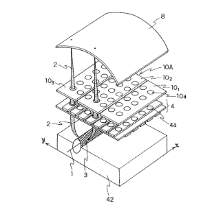
Figs. 8 and 9 are exploded perspective view
and sectional view, respectively, of yet another '
example of the image display apparatus according to the
present invention. In Figs. 8 and 9, too, same numerals
are used to denote same parts of the foregoing Examples
with the descriptions on such parts being omitted. Note
that numeral 9 denotes a luminous element. This Example
is characterized in that both the control electrode 4 and
the focusing electrode 10 are comprised of respective
curved surfaces having a curvature substantially the same
~ .
. . . ".
. :..
t
~
Is . . .
.
' .:.
' ' " .. . . . ~.. . . '. .... . .1 ,. ' ..~.. 1. ; '
" '..'. ... : ~.. .. . ,. .. ;. ... .. . . irl :.. - . ~ ,
~l ~2~4 ~.2
curvature of the front glass, the string like hot cathode
1 and the perforated cover electrode 3 are disposed on a
flat plane, and a second grid 46 is interposed between the
control electrode 4 and the perforated cover electrode
3. The second grid 46 is formed by etching a metallic
plate such as a stainless steel plate to define
electron-pass apertures 46a at even pitch and is shaped
planar, like a second grid as disclosed in, for example,
Japanese Unexamined Patent Publication No. 121014/1993.
To corroborate the effects of the present
Example, the present inventors manufactured a flat-type
image display apparatus having a front glass 8 of 29 in.
in outer size and 24 in. in effective size on an
experimental basis. In the thus manufactured image
display apparatus, the front glass 8, focusing electrode
10 and control electrode 4 comprised respective curved
surfaces having a substantially the same curvature, which
was the curvature of a cylindrical curved surface having a
radius of about 2000 mm, the second grid 46 was made
planar, and the string like hot cathode 1 and the
perforated cover electrode 3 are disposed on a planar back
electrode 42. The string like hot cathode 1 comprised 39
string like hot cathodes arranged at 12. 5 mm pitch in
array (in the direction y of Fig. 8). The distance
between the back electrode 42 and the second grid 46 was
about 15 mm, and the distance between the second grid 46
and the control electrode 4 was about 5 mm at the shortest
and about 20 mm at the longest. The second grid 46
comprised a stainless steel sheet of about 0.2 mm
thickness having about 1.8 mm-square apertures at about 2 '
mm pitch defined by etching. The perforated cover
electrode 3 was formed by etching a stainless steel sheet
of about 0.05 mm thickness to form a mesh configuration
having a rate of hole area of 72 % and hot working the
mesh into an elliptic shape having the minor axis of 2 mm
and the major axis of 3 mm.
The thus manufactured image display apparatus
was found to be substantially improved in lessening the
w . v:..... v
'.' ..' ' ~ ... ', ~ ,.
~:~~'14~~
- 23 --
luminance unevenness in the bridging direction (in the
direction x of Fig. 8) in which the cathodes of the
string like hot cathode 1 extended and in the arrangement
pitch direction (in the direction y of Fig. 8) in which
the cathodes of the string like hot cathode 1 are
arranged. Further, a change in luminance unevenness with
lapse of time was found to be little. Moreover, even in a
operation over a prolonged time period there were not
found phenomena such that emission current of individual
string like cathodes 1 decreased extremely and that the
string like hot cathode 1 was short-circuited to the
perforated cover electrode 3.
In the experimentarily manufactured apparatus,
the ratio of the distance L between the back electrode 4 2
and the second grid 46 to the arrangement pitch P of the
string like hot cathodes 1 was 1.25. When such ratio is
less than 1, the uniformity ratio of electron beam on the
second grid 46 on the string like hot cathode side is
insufficient. This causes the luminance unevenness
particularly in the arrangement pitch direction of
string like hot cathodes to occur conspicuously, in
cooperation with the influence of a variation in the
distance between the second grid 46 and the control
electrode 4. When the ratio exceeds 6, the rate of
electron beam utilized by the second grid at the same
voltage decreases though the uniformity ratio of electron
beam on the second grid 46 on the string like hot cathode
side becomes sufficient. If the application voltage (70 V
in the manufactured apparatus) of the second grid 46 is
set to have a difference of 20 V or less from the ON
voltage (80 V in the manufactured apparatus) of the
control electrode 4, the influence of a variation in the
distance between the second grid 46 and the control
electrode 4 is reduced, thus contributing to a decrease in
luminance unevenness.
Example 6
Fig. 10 is a fragmentary sectional view of yet
. , .. ,: :: : :: ; ;
.,. .,. :. ., ... , :. ..
'
y
... .. ;; .:.. .. ~ ;,;, ~ ,...1 , '
-- 24 -
another example of the image display apparatus according
to the present invention. Example 6 is of the same
arrangement as Example 5 except that the second grid 4 6
is comprised of a curved surface having a curvature
substantially the same curvature of the front glass
8. For instance, the second grid 46 is comprised of a
curved surface having a radius of curvature of about 2000
mm, which is substantially the same curvature of the front
glass 8, and the distance between the second grid 4 6 and
the control electrode 4 is set to 5 mm. In this case, the
distance between the second grid 46 and the perforated
cover electrode 3 is about 15 mm at minimum and about 35
mm at maxmium. Here, electron beam is made uniform and
flat by virtue of the configurations of the string like
hot cathode 1 and perforated cover electrode 3. Hence,
the influence of a variation in the distance between the
second grid 46 and the perforated cover electrode 3 is
little though a gentle luminance unevenness occurs in the
arrangement pitch direction of the string like hot
cathodes 1. Further, the ratio of the distance between
the second grid 46 and the perforated cover electrode 3 to
the arrangement pitch of the string like hot cathodes 1 is
1.25 to 2.9. Such ratio is preferably set within the
range of 1.0 to 6.0, more desirably 1.4 to 3.5. When the
ratio is less than 1, the uniformity ratio of electron
beam on the second grid 46 on the string like hot cathode
side is insufficient, causing keen luminance unevenness.
When the ratio exceeds 6.0, the rate of electron beam
utilized at a fixed voltage decreases.
,
Example 7
Fig. 11 is a fragmentary sectional view of yet
another example of the image display apparatus according
to the present invention. As shown in Fig. 11, Example ?
is of the same arrangement as Example 6 except that the
arrangement pitch of string like hot cathodes 1 is
gradually varied as viewed from the central portion of the
screen to a peripheral portion thereof in accordance with
,;; ; . . ::~,: :: ;:<
y .' .'~~ : .. ' . ' . . .
- 25 -
a variation in the distance between the perforated cover
electrode 3 and the second grid 46. For instance, the
arrangement pitch of string like hot cathodes 1 is
gradually varied so as to assume 8 mm in the central
portion of the screen and 16 mm in a peripheral portion
thereof. Such arrangement allows the density of cathodes
to increase in the central portion largely spaced apart
from the second grid 46 or control electrode 4, hence, the
quantity of electron beam to increase. This contributes
to a further improvement in the uniformity ratio of
electron beam on the second grid 46 on the string like hot
cathode side.
In raising the uniformity ratio of electron beam
sufficiently, the power consumption at the string like hot
cathode 1 and the perforated cover electrode 3 may
increase since the arrangement pitch of string like hot
cathodes 1 has to be decreased. Nevertheless, the power
consumption can be decreased if the back electrode 42 is
divided and driven synchronously with a scanning along a
scanning line so as to control the emission of electron
beam. In this way, the uniformity ratio of electron beam
can assuredly be improved without degrading the
characteristics of the flat-type image display apparatus.
2 5 Example 8
Fig. 12 is a fragmentary sectional view of yet
another example of the image display apparatus according
to the present invention. As shown in Fig. 12, Example 8
is of the same arrangment as Example 5 except that the
pitch of electron-pass apertures 46a of the second grid 46 '
is varied in accordance with a variation in the distance
between the second grid 46 and the control electrode 4.
Further, the rate of hole area of the electron-pass
apertures 46a may be varied. For instance, in a portion
of the second grid corresponding to the central portion of
the display screen the electron-pass apertures 46a
comprise 2.3 mm-square apertures defined at 2.5 mm pitch,
while comprising 1.5 mm-square apertures defined at 1.7 mm
...: .':. ~a-
- 26 -
pitch in a portion of the second grid corresponding to the
peripheral portion of the screen. In this way, the
aperture size and pitch are gradually varied as viewed
from the central portion of the screen to the peripheral
portion thereof. In such arrangement, the electron beam
pass-through efficiency is high in a portion of the second
grid where the aperture pitch or the rate of hole area is
large, assuring a further improvement in the uniformity
ratio of electron beam on the second grid 46 on the
string like hot cathode side in the arrangement pitch
direction of the string like hot cathodes 1.
Although in Example 8 the rate of hole area of
the second grid 46 is varied as viewed from the central
portion of the screen to the peripheral portion thereof in
the arrangement pitch direction of the perforated cover
electrodes 3 and string like hot cathodes l, the rate of
hole area of the perforated cover electrode 3 may be
varied likewise, or the rates of hole area of the
perforated cover electrode 3 and second grid 46 may be
varied at the same time.
Example 9
Fig. 13 is a fragmentary sectional view of yet
another example of the image display apparatus according
to the present invention. As shown in Fig. 13, Example 9
is of the same arrangment as Example 6 except that the
distance between the string like hot cathode 1 and the
perforated cover electrode 3 is gradually varied in the
arrangement pitch direction of the string like hot cathode
1 in accordance with a variation in the distance between
the perforated cover electrode 3 and the second grid 46.
For instance, in the central portion of the display screen
the distance between the perforated cover electrode 3 and
the string like hot cathode 1 on the major axis of the
ellipse is set to 2 mm, while in the peripheral portion of
the display screen it is set to 3 mm. In this way, the
distance between the perforated cover electrode 3 and the
string like hot cathode 1 on the major axis of the ellipse
' v
~
.
. ,
, .
:
.
~:
r
'
,
.
~?1~'~~~2
- 27 -
is gradually increased as viewed from the central portion
of the screen to the peripheral portion thereof. When the
distance between the perforated cover electrode 3 and the
string like hot cathode 1 is small, a large amount of
electrons are drawn out, while when the distance is large,
the amount of electrons drawn out is decreased. Hence, by
facilitating the emission of electron from the string Iike
hot cathode 1 at a location relatively far from the second
grid 46, the uniformity ratio of electron beam on the
second grid 46 on the string Iike hot cathode side is
improved in the arrangement pitch direction of the
string like hot cathodes 1.
Example 10
Fig. 14 is a fragmentary sectional view of yet
another example of the image display apparatus according
to the present invention. As shown in Fig. 14, Example 10
is of the same arrangment as Example 5 except that the
second grid 46 is divided in the arrangement pitch
direction of the string like hot cathodes 1 and the
divided grids are applied with respective voltages which
are different. Like the focusing electrode of Example I,
the second grid 46 is preferably divided into about three
to about nine. For example, the second grid 46 is divided
into five, a divided portion 463 of the second grid 46
which is coincident with the central portion of the
display screen is applied with a voltage of 90 V, and
divided portions 462 and 469 thereof coincident with
peripheral portions of the screen are applied with a
voltage of 60 V. The voltage applied to the second grid
46 is gradually varied so that the variation in potential
of the second grid 46 will be developed gently as viewed
from the central portion to the peripheral portion of the
screen. Such arrangement balances the quantity of emitted
electrons at a portion of the second grid 46 relatively
near the string like hot cathode 1 or the control
electrode 4 since such a portion is applied with a low
voltage. This results in a further improvement in the
t
- 28 -
uniformity ratio of electron beam on the second grid 46 on
the string like hot cathode side.
Example 11
Fig. 15 is a fragmentary sectional view of yet
another example of the image display apparatus according
to the present invention. As shown in Fig. 15, Example 11
is of the same arrangment as Example 10 except that the
second grid 46 is comprised of a curve surface. The
second grid 46 has a curvature substantially the same
curvature of the control electrode 4 and further is
divided in the arrangement pitch direction of the string
like hot cathodes l, the resulting divided grids being
applied with respective voltages which are different. For
example, the second grid 46 is divided into five, a
divided portion 463 of the second grid 46 which is
coincident with the central portion of the display screen
is applied with a voltage of 90 V, and divided portions
462 and 464 thereof coincident with peripheral portions of
the screen are applied with a voltage of 60 V. The
voltage applied to the second grid 46 is gradually varied
so that a variation in potential of the second grid 46
will be developed gently as viewed from the central
portion to the peripheral portion of the screen. Further,
the second grid 46 is comprised of a curved surface having
a radius of curvature of about 2000 mm and is disposed as
spaced by 5 mm apart from the control electrode. Like
Example 10, such arrangement allows the uniformity ratio
of electron beam on the second grid 46 on the string like
hot cathode side to be further improved than in Example 5. '
Although the vacuum enclosure 43 is formed of
glass in the foregoing Examples, it may be a vacuum
enclosure comprising a sealed metallic enclosure instead
of the part of the enclosure 43 other than at least the
front glass 8 to be provided with the luminous element 9,
the front glass 8 being formed integrally with the sealed
metallic enclosure by frit-bonding or like means.
Further, although the string like hot cathodes 1
~:r;:
- 29 -
and the perforated cover electrodes 3 are disposed on a
flat plane in the foregoing Examples, these electrodes may
be disposed on a curved surface having a curvature larger
than that of the inner wall of the vacuum enclosure on at
least the side where the luminous element 9 is provided
unless the reliability of those electrodes is
substantially degraded.
It should be appreciated that although the
cathode comprises a string like hot cathode in Examples 5
to 11, these Examples, like Example 4, may employs a hot
cathode of the structure different from the string like
structure, a cathode of a field emission type electron
gun or a thermionic emission type cathode. Such
arrangment also assures effects similar to those of the
foregoing Examples.
In addition, combining the features of two or
more Examples will afford a further improved image display
apparatus.
As has been described, according to the present
invention the division of the focusing electrode allows
application of different voltages to the divided focusing
electrodes in accordance with the distance between the
focusing electrode and the front glass. Therefore, the
beam diameter of electron beam on the display screen can
be made substantially uniform and minimized over the mire
screen, thus resulting in an effect of displaying a clear
image with a uniform luminance over the entire screen.
Also, it becomes possible to lighten and thin
the vacuum enclosure with ease and to make each electrode
flat and, hence, there is given an effect such that the '
minimization of the manufacturing cost can be realized.
Further, according to the present invention, the
image display apparauts is arranged such that the inner
wall of the vacuum enclosure on at least the side where
the luminous element is provided, namely the luminous
element, the focusing electrode and the control electrode
comprise respective curved surfaces having a substantially
the same curvature, that the second grid is disposed
r...~ ~..;', '-~ ,,wx:. ~... ~..'~:~. -~~. :'« :: ,
SVl 11.e I 1~ ~~ H .. 5~. ,
..Kv..t'sl. , .. W ~. s"~.'~:;'~~C.'~'~e.~,.W .4'..i ':~. ~y:..,~5~i"
4,....,r.,is..> .', ~ ~hun.~ 1h w~Alt '~.~~~W w c .w.:,
'.~ ",\',.~1"1~,.. ~.k~ 1...1,..
21~'~~42
- 30 -
between the control electrode and the perforated cover
electrode, and that the perforated cover electrode and the
cathode are disposed on a curved surface having a
curvature substantially larger than that of the aforesaid
curvature or on a flat plane. Such arrangement offers the
effects of: mitigating deformation of the perforated cover
electrode during operation, the temperature of the
perforated cover electrode being likely to be
significantly elevated due to its location adjacent the
cathode serving as a heat source and the impingement of
electrons thereon; minimizing the luminance unevenness;
reducing the shortening of the cathode life; and improving
the reliability of the perforated cover electrode and that
of the cathode. As a result, a highly reliable image
display apparatus of a prolonged life is obtained which is
capable of displaying a clear image with a uniform
luminance over the entire screen.
Also, by making the second grid have a curvature
substantially the same curvature of the control electrode,
image display with further improved luminance and
luminance uniformity is feasible.
Furthermore, by increasing the arrangement pitch
of the perforated cover electrodes and cathodes as viewed
from the central portion to the peripheral portion of the
screen, the flat-type image display apparatus enjoys
substantially improved luminance uniformity while
minimizing the influence on other characteristics thereof.