Note: Descriptions are shown in the official language in which they were submitted.
sEI ~4-2p
TITLE OF THE INVENTION
COUPLING STRUCTURE OF OPTICAL FIBERS AND OPTTCAL
WAVEGUIDES
BACKGROUND OF THE INVENTION
Field of the Invention
The present invention relates to a coupling structure
of optical fibers and optical waveguides which is used in an
optical communication system as an optical waveguide module
having an optical waveguide circuit.
Related Background Art
In the field of optical communications, for the purpose
of, e.g., processing signals from optical fibers by optical
waveguides, a coupling structure in which the optical
fibers and the optical waveguides are optically coupled is
sometimes needed.
For example, in a conventional coupling structure in
which optical fibers and optical waveguides are coupled by
welding, an optical fiber arrangibg connector in which a
mufti optical fiber extending from a ribbon fiber is
arranged, and a waveguide substrate on which an optical
waveguide layer including a mufti optical waveguide is
formed, are fixed in separate metal members. The end faces
of the optical f fiber arranging connector and the waveguide
substrate respectively fixed in the metal members are
abutted against each other, and the optical f ibe.rs and the
optical waveguides are aligned with each other. Then, the
1
~~2~18~1
SEI 94-20
metal members are welded with each other by using, e. g. , a
YAG laser.
In the above coupling structure, however, since the
metal members are deformed during welding, the optical
waveguides and the optical fibers cause misalignment to
increase the light transmission loss of the coupling
structure. Since the metal members axe used as metal
housings of the optical fiber arranging connector and the
optical waveguide layer, the manufacturing cost becomes
very high. Thus, a demand has arisen for a coupling
structure of optical fibers and optical waveguides free
from these problems.
Tn a conventional coupling structure in which optical
fibers and optical waveguides are coupled by using a
photo-setting (photo-curable) adhesive, a mufti optical
fiber extending from a ribbon fiber is arranged by being
(fixed in, a.g., the V-grooves of a glass optical (fiber
arranqinq connector. A waveguide substrate on which an
optical waveguide layer including a mufti optical waveguide
is formed is mounted in a glass member, and the optical
fibers and the optical waveguides are aligned with each
other. A photo-setting adhesive is injected between the end
faces of the optical fiber arranging connector and the glass
member to be coupled, and light is radiated from the
peripheral portion, thereby setting the photo-setting
adhesive. In order to sufficiently set the photo-setting
2
~~~~1~~~
SEI 94-20
adhesive, as described above, the opl:ical fiber arranging
connector is made of a glass material. (e.g., quartz. glass)
which transmits light having a wavele~ng~th capable of
setting the adhesive (e.g., an ultraviolet-curing resin) at
a high transmittance.
In the above coupling structure, the optical fiber
arranging connector is connected to one or two ends, i.e.,
one or both of the input and output portions, of the
waveguide substrate.
A prior art technique concerning the coupling structure
of optical fibers and optical waveguides in which an optical
fiber arranging connector and a waveguide substrate are
adhered by using a photo-setting adhesive is described in,
e.g. , "IEEE Photonics Technology Letters, vol. 4, No. 8,
pp. 906 - 908, Aug. 1992" in detail. A prior art technique
concerning the coupling structure of optical f fibers and
optical waveguides in which an optical fiber arranging
connector and a waveguide substrate are mechanically ffixed
is described in, e.g. , "Ceramics 29, No. 4, pp. 319 - 321,
1994" in detail.
A prior art technique concerning the coupling structure
of optical fibers and optical waveguides in which optical
fibers are directly fitted in a processed waveguide
substrate is described in, e.g., Japanese Patent Laid-Open
No. 63-279206 (French Patent No. 8,703,385, ri~arch 12,
1987), Japanese Patent Laid-Open No. 1-186905 (French
3
'~~.~~8u1
SEI 94-20
Patent No. 8,716,398, November 26, 1987), and International
Patent Laid-Open No. 4-507153 (French Patent No. 9,002,575,
March 1, 1990) in detail.
A prior art technique concerning the coupling structure
of optical fibers and optical waveguides in which quartz
glass housings respectively incorporating a waveguide
substrate and an optical fiber arranging connector are
welded with each other by heating is described in, a . g. ,
Japanese Patent Laid-Open No. 2-253206 in detail. A prior
art technique concerning the coupling structure of optical
fibers and optical waveguides in which optical fibers are
directly adhered to a waveguide substrate is described in,
e.g., Japanese Patent Laid-Open No. 5-173039 (U.S.A. -
No. 5,185,835, February 9, 1993) in detail.
SUMMARY OF THE INVENTION
However, in the conventional structures in which
coupling is made by using a photo-setting adhesive, a fiber
arranging substrate constituting the optical fiber
arranging connector must be made of a light-transmitting
material, eag., quartz glass, which transmits light having
a wavelength capable of setting the adhesive at a high
transmittance. More specifically, a silicon substrate is
generally used as a fiber arranging substrate because it .can
be processed easily. Then, however, light having a
wavelength capable of setting the adhesive is not
transmitted between the end faces of 'the fiber arranging
4
~~~~c~~~
sm 94-za
substrate and the waveguide substrate at a high
transmittance, and the adhesive remains in the liquid form
in most of the region between the end faces where guarantee
of a high adhesion strength is most important. For this
reason, in the conventional structures, e.g., a quartz
glass plate is used as the fiber arranging substrate. This,
however,. causes another problem of difficult processing.
More specifically, in order to improve the alignment
precision, the arranging substrate must be subjected to
precision grinding to form arranging grooves used for
arranging optical fibers at high precision. This precision
grinding is not easy for existing light-transmitting
materials, e.g., quartz glass. Accordingly, when, e.g., a
quartz glass plate is used as the arranging substrate, the
25 operation of farming the arranging grooves becomes very
cumbersome. Then, the manufacture time of the coupling
structure is prolonged, and it is difficult to arrange
optical fibers at high positional precision.
More specifically, when an optical fiber arranging
connector and an optical waveguide device are coupled by
using a photo-setting adhesive, if the material of the
arranging substrate is selected by considering good
formability of the fiber arranging grooves in the arrang~.ng
substrate, light transmission becomes insufficient, and the
adhesive is not sufficiently set especially between the end
faces of the optical fiber arranging connector and the
5
,..
SEI 94-20
optical waveguide device . Even if the optical f fiber
arranging connector and the optical waveguide device are
aligned before the adhesive is set, misalignment is
increased as time passes or by a temperature change, causing
an increase in light transmission loss and a decrease in
environmental durability. ~7n the other hand, if the
material of the arranging substrate is selected by
considering light transmission, since the optical fiber
arranging grooves are difficult to form, the positional
precision of the optical fiber arrangement is decreased,
and it becomes difficult to align all of the rnulti optical
fiber and the multi optical waveguide at high precision,
causing a decrease in basic characteristics of the optical
device. In this manner, in the conventional optical
coupling structures using a photo-setting adhesive, a
trade-off relationship exists in the manufacture between a
demand for aligning the optical fibers and optical
waveguides at high precision and a demand for maintaining
high reliability of the manufactured optical coupling
structure over time .
A silicon substrate may be employed as the fiber
' arranging substrate by using a thermosetting adhesive in
place of the photo-setting adhesive. However, since the ,
adhesive usually requires at least 30 minutes to thermoset,
the productivity is low. In addition, since an alignment
stage for the optical fibers and the optical waveguides is
6
~~~'~gb~.
SEI 9~-20
deformed by heat, aligned cores cause positional errors
while the adhesive is set.
The present invention has been made in view of the above
problems, and has as its object to provide a coupling
structure of optical fibers and optical waveguides, which
can be manufactured in accordance with a systematic
short-time process, which can align the mufti optical fiber
and the mufti optical waveguide with each other at high
precision, which has a small light transmission loss over
a long period of time, and which has a high environmental
durability against, e.g., a temperature change.
In order to achieve the above object, according to the
present invention, there is provided a coupling structure
of optical fibers and optical waveguides, comprising:
optical fibers; an optical fiber arranging connector having
a first and second members, the optical fibers being
sandwiched by the f first and second members to be f fixed in
the optical fiber arranging connector; a waveguide~device
having a waveguide substrate, optical waveguides being
formed on a surface of the waveguide device, ends of the
waveguides and ends of the optical fiber arranging connector
being aligned with each other by abutting end faces thereof
against each other; and an adhesive interposed and set
between the end faces, the adhesive being a photo--setting
adhesive, the first rneanber being made of a material
preventing light having a wavelength capable of setting the
adhesive from passing
7
J
SET 94-20
therethrough, and in at least part of a region where the end
faces of the optical fiber arranging connector and the
waveguide device oppose to each other,, at least one of the
optical fiber arranging connector and the waveguide device
in the vicinity of the end face thereof being made of a
light-transmitting material through which light having a
wavelength capable of setting the adhesive can pass.
The light-transmitting material may be preferably a
material having a thermal expansion coeff icient of less
than 6 x 10-~ [/K] , more preferably 1 x 10⁻⁵ [/K] . In this
case, it is preferable that the light-transmitting material
is glass containing Si02 as a major component. Especially,
it is preferable that the light-transmitting material is
glass having a thermal expansion coefficient coinciding
with that of silicon within a range of ~20%. It is
preferable that the light-transmitting material is a resin
having a light absorption edge at a wavelength of not more
than 450 nm.
The adhesive may be a photo-setting/thermosetting
adhesive containing a thermosetting initiator in addition
to a photo-setting initiator. In this case, it is
preferable 'that the adhesive is coated to be interposed
between the end face of the optical fiber arranging
connector and the end face of the waveguide device,
photo-set by light radiation, and thereafter thermoset by
heat.
8
'.
AEI 9~--20
The waveguide substrate may have an end face opposing
the end face of the optical fiber arranging connector
through the adhesive, and at least part of the waveguide
substrate in at least the vicinity of the end face thereof
may be made of the light-transmitting material that can
transmit light having the wavelength capable of setting the
adhesive.
The waveguide device may have the waveguide substrate
and a waveguide covering member that covers a surface of the
waveguide substrate on which the optical waveguides are
formed, and the waveguide covering member may have an end
face opposing the end face of the fiber arranging connector
through the adhesive, and at least part of the waveguide
covering member in at least the vicinity of the end face
thereof may be made of the light-transmitting material that
can transmit light having a wavelength capable of setting
the adhesive. In this case, it is preferable that the
light-transmitting material is constituted as part of the
end face of the waveguide covering member opposing the end
face of the optical fiber arranging connector to have a
sectional area of nat less than 1. 0 mmz .
The first member may be a fiber arranging substrate
having a surface on which arranging grooves for the optical
fibers are formed. In this ease, it is preferable that the
f fiber arranging substrate is made of a material having a
thermal expansion coefficient of less than 6 x 10'5 [/K],
9
SEI 94-20
more preferably 1 x 10⁻⁵ [/K] . Especially, it is preferable
that the fiber arranging substrate is made of silicon, and
the arranging grooves are formed by mechanical processing
or anisotropic etching. It is preferable that the fiber
arranging substrate is made of a ceramic material, and the
arranging grooves are formed during sinter ing the ceramic
material.
It is preferable that the fiber arranging substrate is
made of a plastic material, and the arranging grooves are
formed during molding the plastic material. It is
preferable that the plastic material is a phenol resin
containing a f i l ler .
The second member may be a fiber fixing member, adhered
to the fiber arranging substrate, for fixing the optical
fibers in the arranging grooves, and the end face of the
fiber fixing member may oppose the end face of the waveguide
device through the adhesive, and at least part of the fiber
fixing member in at least the vicinity of the end face
thereof may be made of the light-transmitting material that
can transmit light having a wavelength capable of setting
the adhesive.
The first and second members may be integrally farmed
by molding a plastic material. , '
One end face of the waveguide device may oppose an end
face of a f first optical f fiber arranging connector as an
optical input portion, and the other end face of the
SEI 94-20
waveguide device may oppose an end face of a second optical
fiber arranging connector as an optical output portion.
In the coupling structure of the optical fibers and the
optical waveguides of the present invention, the optical
fiber arranging connector is constituted by the first and
second members that fix the optical fibers therein. The
first member is made of a material that does not transmit
light having a wavelength capable of setting the adhesive.
Thus, the first member is not made of a lights-transmitting
material, e.g., quartz glass, but is made of, e.g., silicon,
so that it can be processed easily. Then, the optical fiber
arranging grooves can be formed in the f first member in
accordance with a short-time, simple process at high
positional precision. As the multi optical fiber and the
multi- optical waveguide are aligned with each other at high
precision, a coupling structure having a small transmission
lass in the coupled end faces can be obtained.
In part of a region where the end faces oppose each
other, at least one of the optical f fiber arranging connector
and the waveguide device in the vicinity of the end face
thereof is made of a light--transmitting material that can
transmit light having a wavelength capable of setting the
adhesive. When light is radiated through the
light-transmitting portion made of the light-transmitting
material, a thin film formed by the photo-setting adhesive
interposed between the end faces, especially in the
11
SEI 94-20
vicinity of the coupled end faces, of the optical fibers and
the optical waveguides can be set easily and reliably over
a wide area. If the optical fibers and the optical
waveguides are aligned with each other before the adhesive
is set, this aligned state can be stably maintained.
With the combination of the high processing precision
of the arranging grooves for fixing the optical fibers and
the high setting properties of the adhesive, a coupling
structure having a small light transmission loss over a long
period of time and a high environmental resistance can be
realized.
First, the optical waveguides of the waveguide device
and the optical fibers of the optical fiber arranging
connector are aligned with each other. Subsequently, the
end face of the optical fiber arranging connector is adhered
by polymerization on the end face of the waveguide device
with a photo-setting/thermosetting adhesive. When
polymerization adhesion is completed in this manner, light
is radiated from the peripheral portions of the adhesion
2o surfaces, on which the adhesive is coated, at a
predetermined intensity for a predetermined period of time,
thereby photo-setting the adhesive. Thereafter, the
optical waveguide module is heated at a predetermined
temperature for a predetermined period of time, in order to
thermoset the adhesive, so that the adhesive is
substantially and f finally set and f fixed. Then, the optical
12
~~z~~~~
AEI 94-20
waveguides and the optical f fibers can be f firmly mounted and
fixed with each other.
When the waveguide device has a waveguide covering
member that covers an optical waveguide forming surface on
the waveguide substrate, if the wavegc~ide covering member
made of a light-transmitting material is formed in part of
the connection region of the optical ffiber arranging
connector and the waveguide device to have a sectional area
of 1.0 mm2 or more, this waveguide covering member fixes
part of the adhesion surface which is not completely fixed
during photo-setting. Thus, a fluctuation in loss during
thermosetting reaction is suppressed.
The present invention will become more fully understood
from the detailed description given hereinbelow and the
accompanying drawings which are given by way of
illustration only, and thus are not to be considered as
limiting the present invention.
Further scope of applicability of the present invention
will become apparent from the detailed description given
hereinafter. However, it should be understood that the
detailed description and specific examples, while
indicating preferred embodiments of the invention, are
given by way of illustration only, since various changes and
modifications within the spirit and scope of the invention
will become apparent to those skilled in the art from this
detailed description.
13
w ~:~~'~8~~
SET 94-20
HRTEF DESGRTPTTOI~ OF THE DRAWTIdGS
Fig. 1 is a perspective view shoring the overall
arrangement of a coupling structure of optical fibers and
optical waveguides according to an ernbodiment of the
present invention;
Fig. 2 is an perspective view showing the exploded
arrangement of the main part of the coupling structure of
the optical f fibers and the optical waveguides shown in
Fig. 1;
Fig. 3 is a longitudinal sectional view showing the
structure in the vicinity of the coupled end faces of the
optical fibers and the optical waveguides shown in Fig. 1;
Fig. 4 is a cross-sectional view showing the structure
of the coupled end faces shown in Fig. 3;
Figs . 5 and 5 are longitudinal sectional views showing
the structure of a modif ication of the coupling structure
of the optical f fibers and the optical waveguides shown in
Fig. 1, in which the end faces of an arranging substrate and
a waveguide substrate are adhered to each other;
Figs . 7 to 9 are longitudinal sectional views showing
the structure of a modification of the coupling structure
of the optical fibers and the optical waveguides shown in
Fig. 1, in which the end faces of a fixing member and a '
waveguide substrate are adhered to each other;
Figs . 10 to 15 are longitudinal sectional views showing
the structure of a modification of the coupling structure
14
FEZ 9~-20
of the optical f fibers and the optical waveguides shown in
Fig. 1 in which the end faces of an arranging substrate and
a waveguide substrate and the end faces of a fixing member
and a covering member are adhered to each other;
Figs . 17 to 23 are longitudinal sectional views showing
the structure of a modification of the coupling structure
of the optical fibers and the optical waveguides shown in
Fig. 1, in which the end faces of an arranging substrate and
a covering member and the end faces of a fixing member and
a waveguide substrate are adhered to each other;
Fig. 24 is a longitudinal sectional view showing the
structure of a modification of the coupling structure of the
optical fibers and the optical waveguides shown in Fig. 1 in
the vicinity of the coupled end faces, in which the end
faces of an arranging substrate and a waveguide substrate
are adhered to each other;
Fig. 25 is a cross-sectional view showing the structure
of the coupled end faces, in which the fixing member of
Fig. 24 has a flat shape;
Fig. 2fi is a cross-sectional view showing the structure
of the coupled end faces, in which the fixing member of
Fig. 24 has a U-shaped section;
Fig. 27 is a perspective view showing the exploded '
arrangement of the main part of Fig. 2fi;
Figs . 28 to 30 are cross-sectional views showing the
structure of the coupled end faces of a modification of the
z~z~~~~
AEI 94-20
coupling structure of the optical fibers and the optical
waveguides shown in Fig. 1, in which the fixing member and
the arranging substrate have various :shapes;
Fig. 31 is a graph showing a relationship between the
wavelength of incident light and the light transmit lance of
each of various types of light-transrnitting materials;
Fig. 32 is a sectional view showing the step of forming
a resin or the like around optical fibers in an optical
fiber arranging connector by molding;
Fig. 33 is a graph showing a relationship between a
misalignment amount and a light transmission loss in a
coupling structure of a single-mode fiber and an optical
waveguide;
Fig. 34 is a cross-sectional view showing the structure
of the coupled end faces of the coupling structure of
optical fibers and optical waveguides according to Example
1 of the present invention;
Fig. 35 is a schematic arrangement diagram showing the
arrangement of a measuring system that performs a heat cycle
test of a coupling structure of optical fibers and optical
waveguides;
Fig. 36 is a graph showing a fluctuation over 'time of
the light transmission loss of two fiber-fitted optical '
waveguides which are arbitrarily selected from eight
optical waveguides in the coupling structure of the optical
fibers and the optical waveguides of Example 1;
16
SEI 94-20
Fig. 37 is a graph showing a fluctuation over time of
the light transmission loss of two fiber-fitted optical
waveguides which are arbitrarily selected from eight
optical waveguides in the coupling structure of the optical
fibers and the optical waveguides of Comparative Example 1;
Fig. 38 is a plan view showing the overall arrangement
of the coupling structure of optical fibers and optical
waveguides aecqrding to Example 3 of the present invention;
Fig.w39 is a side view of the coupling structure of
Fig. 38;
Fig. 40 is a bottom view of the coupling structure of
Fig. 38;
Fig. 41 is a cross-sectional view showing the structure
of a waveguide substrate shown in Figs. 38 to 40;
Figs . 42 to 44 are plan views showing the arrangement of
an optical waveguide layer in the waveguide substrate shown
iri Figs. 38 to 40;
Fig. 45' is a graph showing a theoretical relationship
between a misalignment amount and a light transmission loss
in the coupling structure of optical fibers and 'optical
waveguides;
Fig. 46 is a graph showing a change over time in preset
temperature in a heat cycle test conducted for a coupling
structure of optical (fibers and optical waveguides of
Example 3;
Fig. 47 is a perspective view showing the overall
17
~~.~'r8~1
SEI 94-20
arrangement of a coupling structure o:f optical fibers and
optical waveguides according to Example 4 of the present
invention;
Fig. 48 is a table showing a fluctuation in light
transmission loss obtained after the adhesive is photo-set
and after the adhesive is thermoset in a coupling structure
of the optical f fibers and the optical waveguides shown in
Fig. 47; and
Fig. 49 is a table showing a thermal expansion character
and a light absorption character of various types of
materials used in the optical waveguide module.
DESCRIPTION OF THE PREFERRED EMBODIMENT
The arrangement and function of the preferred
embodiment of the present invention will be described in
detail with reference to Figs. 1 to 48. In the description
of the drawings, the same components are denoted by the same
reference numerals, and a repetitive description will be
omitted. The ratio of the size shown in the drawings does
not necessarily coincide with that given by a description.
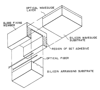
Fig. 1 is a perspective view showing the overall
arrangement of a coupling structure of optical fibers and
optical waveguides according to an embodiment of the
present invention. Fig. 2 is an perspective view showing
the exploded arrangement of the main part of the coupling
structure of the optical fibers and the optical waveguides
shown in Fig. 1. In this coupling structure of the optical
18
21~"1g~1
sEZ 94-zo
fibers and the optical waveguides, as skiown in Fig. 1,
optical f fiber arranging connectors 1 and a waveguide device
3 are fixed to each other with an ultraviolet-curing resin
i
adhesive 4 by abutting their end face:: against each other.
As shown in Fig . 2 , each optical f fiber arranging
connector 1 is constituted to have a fixing plate 11 made of
quartz glass and formed with a recessed portion so that it
has a substantially U-shaped section, and an arranging
substrate 1Z made of silicon and formed to have such a size
that it is fitted in this recessed portion. Five arranging
grooves 131 to 135 having a V-shaped section are formed in
the lower surface of the arranging substrate 12 parallel to
each other at the same interval . Five optical f fibers 211 to
215 extending from a ribbon fiber 2 entirely covered with a
resin are buried in these arranging grooves 131 to 135. when
the arranging substrate 12 is fitted in and fixed in the
recessed portion of the fixing plate 11, the five optical
fibers 211 to 215 are aligned in an array and held.
The waveguide device 3 is constituted to have a silicon
waveguide substrate 31 and a light-transmitting waveguide
covering member 32 provided on the waveguide substrate 31.
A thin optical waveguide layer 33 is formed on the upper
surface of the waveguide substrate 31, i.e., on the surface
of the waveguide substrate 31 contacting the waveguide
2~ covering member 32 ( this waveguide covering member 32 is not
an indispensable element of the present invention as will
19
~1~'~8~ ~
SET 94-20
be described later) , to be integral with the waveguide
substrate 31. Five optical waveguides 341 to 345 are formed
in the optical waveguide layer 33 to serve as cares.
The optical waveguide layer 33 is generally formed by
forming an Si02 glass layer (cladding :Layer) on a silicon
substrate (waveguide substrate 31) by the flame deposition
method, depositing an Si02 layer containing a dopant and
having a high refractive index on the SiOz glass layer and
etching this SiOz layer, thus forming Bores (the optical
waveguides 341 to 345) , and depositing an Sia2 layer serving
as an upper cladding layer. Accordingly, the arrangement
pitch of the optical waveguides 341 to 345 can be set at high
precision to coincide with the arrangement pitch of the
optical f fibers 211 to 215 of the optical f fiber arranging
connector 1.
In this coupling structure of the optical fibers and the
optical waveguides in which the end faces of the optical
fiber arranging connector a and the waveguide device 3 are
abutted against each other and fixed with the resin adhesive
4, the end face of the silicon arranging substrate 12
opposes the end face of the light-transmitting waveguide
covering member 32, and the end face of the silicon
waveguide substrate 31 opposes 'the end face of the
quartz-glass fixing plate 11. Part of the resin adhesive 4
not only swells to be present on the outer peripheral
portions of the end faces of the optical fiber arranging
aEI 94-20
connector 1 and the waveguide device 3 but also is present
between these end faces as a thin film.
The first characteristic feature of this embodiment is
that the arranging substrate 12 is formed by processing a
silicon wafer. As silicon can be easily precision-ground,
the arranging grooves 131 to 135 can be formed at high
positional precision by using a diamond blade or the like.
The arranging grooves 131 to 135 can also be formed to have
a correct v shape at high positional precision by applying
an anisotropic etching technique of the semiconductor
process.
The second characteristic feature of this embodiment is
that both the f fixing plate 11 f fixed on the arranging grooves
131 to 135 and the waveguide covering member 32 arranged on
the upper portion of the waveguide substrate 31 are made of
a light-transmitting material (e.g., quartz glass or
ultraviolet-transmitting resin), and that the arranging
substrate 12 and the waveguide substrate 31, which are made
of silicon and which do not transmit ultraviolet rays and
visible light respectively, oppose the fixing plate 11 and
waveguide covering member 32, which transmit ultraviolet
rays and visible light respectively. For this reason, when
the resin adhesive 4 is interposed between the end faces of
the optical f fiber arranging connector 1 and the waveguide
device 3 and light is . radiated through the
light-transmitting (transmits light having a wavelength
21
~~.~~'1~~~.
SET ~4-20
capable of setting the resin adhesive 4) fixing plate 11 and
waveguide covering member 32, not only the exposed resin
adhesive 4 but also the thin film of t:he resin adhesive 4
between the end faces is set, thereby firmly fixing the
optical fiber arranging connector 1 and the waveguide
device 3 with eacl~. other.
Therefore, according to this embodiment, with the
combination of the above two characteristic features, the
following remarkable effects can be obtained.
First, since the arranging substrate 12 is made of
silicon, the arranging grooves 131 to 135 can be formed ~to
have a highly precise shape at accurate positions, so that
the optical f fibers 211 to 215 can be arranged at high
precision only by fixing the fixing plate 11. hence,
alignment of the optical f fibers 211 to 215 with the optical
waveguides 341 to 345 in a step before setting the resin
adhesive 4 can be performed easily at high precision.
Second, since the resin adhesive 4 can 'be set well even
between the end faces, the aligned state can be stably held.
That is, since misalignment is not caused even if a stress
acts due to mechanical impact and temperature change during
use, the light transmission characteristics can be
maintained over a long period of time . °
Fig. 3 is a longitudinal sectional view showing the
structure in the vicinity of the coupled end faces of the
optical fibers and the optical waveguides shown in Fig. 1.
22
SEI 94-20
Fig. 4 is a cross-sectional view showing the structure of
the coupled end faces shown in Fig. 3. As shown in Fig. 3,
if one of the elements constituting the opposing end faces
has light transmission properties, the resin adhesive 4 at
this portion is set. Hence, the set adhesive covers a wide
range, as indicated by a hatched portion in Fig. 4.
In addition to this embodiment, various modifications
can be made . These modifications will be described with
reference to longitudinal sectional views of Figs. 5 to 23.
Figs . 5 and s are longitudir~.al sectional views showing
the structure of a modification in which the end faces of an
arranging substrate and a waveguide substrate are adhered
to each other . Figs . 7 to 9 are longitudinal sectional
views' showing the structure of a modification in which the
end faces of a fixing member and a waveguide substrate are
adhered to each other. Figs. 10 to 16 are longitudinal
sectional views showing the structure of a modif ication in
which the end faces of an arranging substrate and a
waveguide substrate and the end faces of a fixing member and
a covering member are adhered to each other. Figs. 17 to 23
are longitudinal sectional views showing the structure of
a modif ication in which the end faces of an arranging
substrate and a covering member and the end faces of a
f fixing member and a waveguide substrate are adhered to each
other.
The expression of the drawings will be described. A
23
SEI 9~-20
fiber arranging substrate made of sil:i~con is indicated by
a cross-hatched portion in the lower 7.eft portion in the
drawings, and optical fibers are buried in the arranging
grooves in the upper surface of the fiber arranging
substrate . A f fiber f fixing member is set on the upper
surface of the optical fiber arranging substrate, and the
optical fibers and the optical waveguides of the waveguide
substrate are aligned with each other.
A blank portion indicates a light-transmitting material
(a material that transmits light capable of setting a
photo-setting adhesive, e.g., quartz glass), a hatched
portion indicates a material that does not transmit light
(e.g. , silicon) , an adhesive shown as a solid portion
indicates a photo-set adhesive, and an adhesive shown as a
hatched portion indicates a liquid adhesive.
If the waveguide substrate has light transmission
properties, the adhesive is set at least at the end face of
the waveguide substrate, so that coupling can be made firmly
(see Figs. 5, 6, ?, 8, 10, 12, 14, 16, 17, 19, 21, and 23).
The same applies to a case wherein the waveguide covering
member has light transmission properties (see Figs. 10, 11,
14, 15, 17, 18, 21, and 22) . In contrast to these, if only
the fixing member is transparent, good coupling can be made
only when its end face opposes the end face of the waveguide
substrate or waveguide covering member (see, e.g., Figs. 9,
13, 20).
2~
z~~~~~~.
SEI 94-20
If only the waveguide covering member has light
transmission properties, from the vie~arpoint of the coupling
strength of an optical fiber arranging connector and a
waveguide device, the area of the end face of the waveguide
covering member opposing the optical fiber arranging
connector is preferably about 1/3 or more the area of the
end face of the waveguide substrate opposing the optical
f fiber arranging connector ( see, a . g. , Figs . 15 , 22 ) .
The coupling structure of the present invention relates
to a structure in which ~n adhesive interposed as a film in
at least part of a portion between the opposing end faces of
an optical fiber arranging connector and waveguide device,
can be set. 4dhen the shapes of the end faces are changed,
the position of the adhesive becomes different accordingly.
More specifically, even if a waveguide covering member
having light transmission properties is not provided and a
f fiber arranging substrate and a waveguide substrate are
both made of silicon and oppose each other (such a structure
is not shown in Fig. S or 4), the coupling structure falls
within the scope of the arrangement of the present invention
depending on the shape of the end face of the
light-transmitting f fiber f fixing plate ( f fixing member ) , as
shown in Figs . 24 to 27 . '
Fig. 24 is a longitudinal sectional view showing the
structure of a modification in the vicinity of the coupled
end faces, in which the end faces of an arranging substrate
SEI 94-20
and a waveguide substrate are adhered to each other. Fig.
25 is a cross-sectional view showing the structure of the
coupled end faces, in which the fixirxg member of Fig. 24 has
a flat shape. Fig. 26 is a cross-sectional view showing the
structure of the coupled end faces, in which the fixing
member of Fig. 24 has a U-shaped section. Fig. 27 is an
exploded perspective view showing the arrangement of the
main part of Fig. 26.
As shown in Fig. 25, when the fixing member made of
glass has a flat shape, its end face to oppose the silicon
waveguide substrate cannot be almost preserved, and the
interposed adhesive is set only slightly. However, as shown
in Figs. 26 and 27, when the fixing member made of glass has
a U-shaped section, an adhesive interposed in a wide area
between the end faces (hatched region in Fig. 26) of the
silicon waveguide substrate and the projecting portions of
the fixing member is set.
Therefore, various modifications exist regarding the
shapes of the end faces of the optical fiber arranging
connector and the waveguide device. The coupling structure
of the present invention is realized by their combinations.
Figs . 28 to 30 are cross-sectional views showing the
structure of the coupled end faces of a modification, irr
which the fixing member and the arranging substrate have
various shapes. In this manner, the end face of the optical
fiber arranging connector can have various shapes. The same
26
SEI 94-20
also applies to a waveguide device.
The adhesive adopted in the present invention may be a
photo-setting adhesive and is not limited to the
ultraviolet-curing resin described above. For example, a
visible light-setting resin which is set upon incidence of
visible light can be adopted. Also, a
photo-setting/thermosetting adhesive to which a heat-curing
catalyst is added in advance can be adopted. As a
photo-setting adhesive, the Luxtrak Series (manufactured by
ICI Co. , tJ.K. ) adhesives are suitable, and especially one
marketed as "LCR509A" (tradename) is preferable.
The light-transmitting material that can be adopted in
the present invention is not limited to quartz glass
containing Si02 as the ma jor component, but any
1.5 light-transmitting material can be used as far as it can
transmit light having a wavelength capable of setting the
photo-setting adhesive as described above. For example, a
resin, e.g., polycarbonate (PC) or polymethyl methacrylate
(PI~3A), whose light absorption edge is at a wavelength of
450 nm or less can be adopted. Especially, the
light-transmitting material is preferably a material having
a thermal expansion coefficient of less than 6 x 7.0-5 [/K],
more preferably 1 x 10⁻⁵ [/K] . The light-transmitting
material is also preferably glass having a thermal
expansion coefficient which coincides with that of silicon
within the range of ~20~ .
27
sEZ 9.4-20
zn the coupling structure of the present invention, the
photo-setting adhesive interposed as a film between the end
faces is set by radiating light through a
light-transmitting material. Hence, the light-transmitting
material to be used must be selected in accordance with the
type of adhesive employed.
Fig. 31 is a graph showing a relationship between the
wavelength of incident light and the light transmit ~tance of
each of various types of light-transmitting materials. As
ZO is apparent from this graph, polycarbonate and PIMA are
suitable for setting a visible light-setting resin, and
quartz glass is suitable for setting both an
ultraviolet-curing resin and a visible light-setting resin.
The fiber arranging substrate that can be adopted in the
present invention is not limited to one described above
which is made of silicon, but can be made of any material as
far as the arranging grooves described above can be easily
formed in it. For example, a ceramic material can be
adopted if arranging grooves are formed in it during
sintering. P~. plastic material can also be adopted if
arranging grooves are formed in it during molding.
Especially, a phenol resin containing a filler, a liquid
crystal polymer formed as an riID Molded Interconnection
Device), and the like are suitable as the plastic materials.
It is preferable that the fiber arranging member is made of
a material having a thermal expansion coefficient of less
28
\. .
sEZ 9~-zo
than 6 x 10'5 [/K] , more preferably 1 ~c 10'5 [/K] .
The f fiber arranging connector that can be adopted in the
present invention is not limited to one which is constituted
by sandwiching optical fibers with separately formed fixing
member and arranging substrate, as described above, and one
which is constitwted by forming a resin or the like around
optical fibers can be employed by molding.
Fig. 32 is a sectional view showing the step of forming
a resin or the like around optical fibers in an optical
fiber arranging connector by molding. A plurality of
optical f fibers extending from a ribbon f fiber 2 are arranged
parallel to each other at the same interval. Metal die
frames 61 and 62 are abutted against each other and fixed so
that these optical f fibers are inserted in the hollow
internal portion defined by them. A resin 60 is injected
into the region surrounded by the die frames 61 and 62 and
cooled. Subsequently, the die frames 61 and 62 are removed
from the optical fibers, and one end face of the resin 60
from which the optical fibers project is mechanically
polished. In this manner, an optical fiber arranging
connector which is integrally formed by molding is
completed.
with the above arrangement, according to the present~
invention, a coupling structure having very high alignment
precision can be xealized. Misalignment is one of the major
factors that causes a light transmission loss. Especially,
29
~1~'~8s~.
SEI 94-20
in order to connect a single-mode fiber and an optical
waveguide with a low loss, alignment is preferably
performed with an alignment precision of 0.5 dam or less.
This value is determined by also considering factors
(misalignment of connected end faces, the distance between
the end faces, and the like) other than misalignment, which
usually cause a loss .
Fig. 33 is a graph showing a relationship between a
misalignment amount and light transmission loss in a
coupling structure of a single-mode fiber and an optical
waveguide. It is apparent from this graph that the larger
the misalignment amount, the larger the loss.
Fig. 49 is a table showing a thermal expansion character
and a light absorption character of various types of
materials used in the optical waveguide module. In
accordance with this table, Si, Y-ZrOZ of the ceramic
material and a phenol resin containing a filler of the
plastic material are suitable as a material constituting a
fiber arranging substrate for having a comparative low
thermal expansion coefficient. Si02, SD1, SD2 of the
glasses containing SiOz as a major component (goods
manufactured by HOYA Co. ), PMMA and PC reinforced by glass
fibers are suitable as a light transmitting material for
having a comparative low thermal expansion coefficient and
a light absorption edge positioning at a wavelength of 450
nm or less .
SEI 9~-20
Tn order to confirm the usefulness and practicality of
the coupling structure according to the present invention,
the present inventors made coupling structure samples as
follows. These coupling structure samples will be
described as examples and comparative examples.
Example 1
Fig. 34 is a cross-sectional view showing the structure
of the coupled end faces of the coupling structure of
optical f fibers and optical waveguides according to Example
1 of the present invention. Although Figs. 1 to 4 can be
referred to in order to understand the coupling structure
of the optical f fibers and the optical waveguides of Example
1, the arrangement of the coupling structure of Example 1 is
slightly different from that of Figs. 1 to ~. The end faces
of a f fiber f fixing plate 11 and a f fiber arranging substrate
12 have the same shape as those shown in Fig. 30. As shown
in Fig. 34, the coupling structure of this example does not
have a waveguide covering member, and the end faces of the
fiber fixing plate 11 made of quartz glass and a waveguide
substrate 31 made of silicon oppose each other. An
epoxy-based ultraviolet-curing resin 4 is used as the
adhesive, and the fiber arranging substrate 12 is made of
silicon. °
An optical f fiber arranging connector 1 is constituted
by the fiber arranging substrate 12 made of silicon and the
f fiber f fixing member 11 made of quartz glass . The f fiber
31
~~~~1~~~.
SEI 94-20
arranging substrate 12 is formed with a recessed portion to
have a substantially U-shaped section, as shown in Fig. 34,
and grooves 131 to 138 having a V-slxape~d section are formed
parallel to each other in the lower surface of the recessed
portion. The V-grooves 131 to 138 are continuously formed
at once by grinding with a diamond blade to have a depth of
150 ~m and a pitch of 250 dam. Eight optical fibers 211 to 218
(having an outer diameter of 125 ~m and a core diameter of
50 ~m in accordance with CCITT standards ) are buried in the
V-grooves 131 to 138 . The f fiber f fixing member 11 is f fitted
under pressure in the recessed portion of the fiber
arranging substrate 12 to f ix the optical f fibers 211 to 218 .
In this example, the fiber fixing member 11 was adhered to
the arranging substrate 12 by using the epoxy-based
ultraviolet-curing resin ~. More specifically, the resin
is coated on the adhesion surface of the fixing member 11 to
be adhered with the fiber arranging substrate 12, and
ultraviolet light having a wavelength of 365 nm emerging
from a high-pressure mercury lamp was caused to be incident
on the adhesive through the quartz glass fixing member 11
and set, thereby adhering the fixing member 11 with the
arranging substrate 12 . The optical f fiber 211 to 218 are
arranged in an array in the optical f fiber arranging '
connector 1 obtained in this manner. The end face of the
optical fiber arranging connector 1 was shaped by optical
polishing so that no misalignment of the coupled end faces
32
SET 94-ZO
will occur without increasing a loss.
A waveguide device 3 is obtained by forming an 8-
optical waveguide layer 33 on the silicon waveguide
substrate 31. A waveguide covering member is not provided,
as described above. The optical waveguide layer 33 is
constituted by a cladding layer 35 made of SiOz--BZ03-Pzo$
glass, and eight optical waveguides 341 to 34$ made of
SiOz-GeOz-Pz05-Bz03 glass, provided at a pitch of 250 x-0.5 dam,
and formed as rectangular prisms having a length of 4 cm (a
section of 8 x 8 pamj . These optical waveguides 341 to 348
serve as cores. Tn this example, the difference in specific
refractive index between the cores and the cladding layer
was set to 0 . 3% .
The end faces of the optical fiber arranging connector
1 and the waveguide device 3 are abutted against each other
to align the optical fibers 211 to 218 and the waveguide
substrates 311 to 318 with each other at once . The
epoxy-based ultraviolet-curing resin 4 is injected between
the end faces of the optical fiber arranging connector 1 and
the waveguide device 3 and set, so that the optical f fiber
arranging connector 1 and the waveguide device 3 are f fixed
with each other, thereby forming the coupling structure of
the optical f fibers and the optical waveguides of this '
example. Tn order to promote setting of the film-like
adhesive interposed between the end faces, 'the end face of
the f fiber f fixing member 11 made of quarts glass opposes the
33
~~.~Yl g~1
SET 94-20
end face of the silicon waveguide substrate 31. Ultraviolet
light having a wavelength of 365 nm ar,~d emerging from the
high-pressure mercury lamp was radiated from the peripheral
ultraviolet-curing resin portion, thereby setting the
ultraviolet-curing resin. Regarding the high-pressure
mercury lamp, Toscure 201 (manufactured by Toshiba Raytech)
was used as an ultraviolet light source.
The coupling structure of the optical fibers and the
optical waveguides of this example includes eight
f fiber-fitted optical waveguides in which the optical f fibers
211 to 218 and the eight optical waveguides 341 to 34$ are
coupled. When the light transmission loss of the
fiber-fitted optical waveguides was measured, the average
loss was 0.18 dB. When the ambient temperature of the
coupling structure was repeatedly cycled (1 cycle = 6 hours)
in the range of -10 to 70°C, a fluctuation over time of the
loss was stable and small, and the fluctuation value fell
Within the range of ~0.1 dB. These are both good results.
The former result represewts the high alignment precision
of mufti connection of the optical f fibers and the optical
waveguides of the coupling structure of this example, and
the 7.atter result represents a high environmental
resistance of the coupling structure of this example.
Fig. 35 is a schematic arrangement diagram showing the
arrangement of a measuring system that performs a heat cycle
test of a coupling structure of optical fibers and optical
34
SEI 94-20
waveguides. An optical waveguide module 71 formed in
Example 1 is provided in a constant temperature tank 70, and
ribbon f fibers 2 serving as the input and output portions of
the optical waveguide module 71 extend to the outside of the
constant temperature tank 70. One ribbon fiber 2 is
connected, by fusing, to an optical fiber 73 connected to
the light-emitting portion of an LED 72. The other ribbon
fiber 2 is connected, by fusing, to an optical fiber 74
connected to the light-receiving portion of an optical
power meter 75. The output portion of the optical power
meter 75 and the input portion of a PC 76 are electrically
connected to each other. With this arrangement, the optical
waveguide module 71 as the measurement target is held at a
predetermined temperature set in the constant temperature
water tank 70. Light emitted from the LED 72 to have a
predetermined wavelength is transmitted in the optical
waveguide module 71 through the optical fiber 73; and is
detected by the optical power meter 75 through the optical
fiber ?4. A detection signal output from the optical power
meter 75 is input to the PC ?6 and, subjected to a
predetermined arithmetic operation, and is displayed on the
standard monitor of the PC 76.
Fig. 36 is a graph showing a fluctuation over 'time of~
the light transmission loss of two fiber-fitted optical
waveguides which are arbitrarily selected from eight
optical waveguides in the coupling structure of the optical
SEI 94-20
f fibers and the optical waveguides of lExample 1.
Example 2
In the coupling structure of the optical fibers and the
optical waveguides of this example, the type of
transmitting material constituting a fiber fixing member 11
is different from that of the coupling structure of Example
1. In this example, polycarbonate as a kind of resin was
used as the light-transmitting material. Tn adhesion of an
optical fiber arranging connector 1 and a waveguide device
3, an epoxy-based visible light-setting resin was used as
the adhesive, and visible light was caused to be incident on
the adhesive through the fiber fixing member 11, thereby
setting the adhesive. The epoxy-based visible
light-setting resin was also used as an~ adhesive for
adhering the f fiber f fixing member 11 on a f fiber arranging
substrate 12. Except far these differences, the
arrangement of the coupling structure of the optical fibers
and the optical waveguides of this example is the same as
that of Example 1.
When the loss of the eight fiber-fitted optical
waveguides included in the coupling structure of Example 2
was measured, the average loss was 0.20 dB. When the
ambient temperature was subjected to the same temperature
cycle as that of Example 1, a result almost the same as that
of Example 1 was obtained. More specifically, a fluctuation
over time of the loss was stable and small, and fell within
36
~~.~'l8(~.1
AEI 9~-zo
the range of ~0.1 dB. These are both good results.
Comparative examples will be described. The coupling
structures of the comparative examples to be described
hereinafter are similar to that of Example 1 in its
arrangement, in the shapes of a fixing member 11, an
arranging substrate 2, and a waveguide substrate 31, and in
that the fixing member 11 and the waveguide substrate 31
oppose each other. ~iowever, Comparative Examples 1 and 2
are different from Example 1 in the materials constituting
the f fixing member 11 and the arranging substrate 12 ,
respectively. An epoxy-based ultraviolet-curing resin was
used as the adhesive in the same manner as in Example 1.
Comparative Example 1
In the coupling structure of optical fibers and optical
waveguides of Comparative Example 1, a fiber fixing member
11 is made of silicon, unlil~e in Examples 1 and 2. Except
for this, the coupling structure of Comparative Example 1
is the same as that of Example 1. Accordingly, in the
coupling structure of this comparative example, a material,
a . g. , quarts glass, which transmits ultraviolet rays at a
high transmittance is not used.
When the loss of the eight fiber-fitted optical
waveguides of the coupling structure of this comparative
example was measured, ~th.e average loss was 0.25 dB. When
the ambient temperature was subjected to the same
temperature cycle as that of Example 1 by using the
37
SEI 94-20
measuring system shown in Fig. 35, the loss fluctuated as
time passed.
Fig. 37 is a graph showing a fluctuation over time of
the light transmission loss of two fiber-fitted optical
waveguides which are arbitrarily selected from eight
optical waveguides in the coupling structure of the optical
f fibers and the optical waveguides of Comparative Example 1.
These losses tended to increase after each cycle, and an
increase in loss exceeding 0.7 dB was observed.
Comparative Example 2
In the coupling structure of optical fibers and optical
waveguides of Comparative Example 2, a (fiber arranging
substrate 11 is made of quartz glass, unlike in Examples 1.
and 2. Except for this, the coupling structure of .
Comparative Example 2 is the same as that of Example 1.
When the loss of the eight fiber-fitted optical
waveguides of this coupling structure was measured, the
maximum value was as large as 1.25 dB while the minimum
value was 0.15 dB, and the average value was 0.52 dB.
.As described above, in the coupling structure of
Comparative Example 1, since a light-transmitting material,
e.g., quartz glass, was not used, ultraviolet light was not
sufficiently incident on the ultraviolet-curing resin. °
Thus, the resin was not sufficiently set, increasing a light
transmission loss and decreasing environmental resistance.
In contrast ~.o this, in 'the coupling structures of
38
SEI 94-20
Examples 1 and 2, since the end face of the fixing member 11
made of quartz glass and the end face of the waveguide
substrate 31 made of silicon oppose each other, the
film-like photo-setting adhesive interposed in the vicinity
of the coupled end faces of the optical fibers 211 to 21g and
the optical waveguides 341 to 34a can be easily and reliably
set. As a result, a coupling structure having a small light
transmission loss and a high environmental resistance, as
described in the examples, can be realized.
In the coupling structure of Comparative Example 2,
since quartz glass as the light-transmitting material is
used as the material of the fiber arranging substrate, the
light-transmitting material is sufficiently set. When,
however, the processing precision of the V-grooves formed
in the arranging substrate was examined, although the
V-groove formed first had a depth of 150 Vim, the V-groove
formed last had a depth of as small as 140 p~m. This is due
to the wear of the blade caused by the difficult
processability of quartz glass. As the processing
precision of the V-grooves was poor, the alignment
precision was degraded, leading to a loss of as large as
1.25 dH.
In order to improve this, the V-grooves must be formed
at high precision. However, with a light-transmitting
material, e.g., quartz glass, it is difficult to arrange
optical fibers at high positional precision, and the
39
w
SEI 94-20
forming operation becomes very cumbersome, thereby
prolonging the manufacturing time of the coupling
structure.
In contrast to this, in the coupling structures of
Examples 1 and 2, since the arranging substrate 12 is made
of silicon that can be processed easily, the v-grooves are
formed at high positianal precision within a short period
of time and in accordance with a simple process. Moreover,
the mufti optical fiber and the mufti optical waveguide are
aligned at high precision, thereby realizing a coupling
structure having a small light transmission loss in the
coupled end faces.
As has been clarified through the comparison with the
comparative examples, in the coupling structures of the
optical fibers 211 to 218 and the optical waveguides 341 to
348 according to Examples 1 and 2 of the present invention,
the fiber arranging substrate 12 made of silicon and the
fiber fixing member 3.1 made of a light-transmitting
material are provided. Thus, the optical fibers are
arranged at high positional precision although the
arranging substrate is manufactured in accordance with a
systematic short-time process, so that the mufti optical
fiber and the mufti optical waveguide can be aligned with
each other at high precision, and the photo-setting
adhesive is easily and reliably set. As a result, a
coupling structure of optical fibers and optical waveguides
>1~'~~~~.
SET 94-20
which has a small light transmissian loss aver a long period
of time and a high environmental resi:~tance against, e.g.,
a temperature change, can be realized.
Example 3
Fig. 38 is a plan view showing the overall arrangement
of the coupling structure of optical fibers and optical
waveguides according to Example 3 of the present invention.
Figs . S9 and 40 are a side view and a bottom view,
respectively, of. Fig. 38: In the coupling structure of the
optical fibers and the optical waveguides of this example,
when an optical f fiber arranging connector 1 and a waveguide
device 3 are to be connected to each other, a
photo-setting/thermosetting adhesive 4 is used.
The optical f fiber arranging connector 1 is constituted
by a fiber arranging substrate 12 made of silicon and a
fiber fixing member 11 made of quartz glass. A plurality of
arranging grooves having a V-shaped section are formed
parallel. to -each other in the lower surface of the recessed
portion formed in the fiber arranging substrate 12 to have
a substantially U-shaped section. A plurality of optical
fibers extending from .a ribbon fiber 2 are buried in the
arranging grooves of the f fiber arranging substrate 12 and
pressed by the f fiber f fixing member 11 f fitted in the recessed
portion of the fiber arranging substrate 12. The end faces
of the optical f fibers are exposed at one end of the optical
f fiber arranging connector 1.
41
SEI 94-20
Regarding the size of the optical fiber arranging
connector 1, the length ( Ll ) , width ( H11 ) , and height ( Hl ) are
about 8 mm, 5 mm, and 2 mm, respectively. The ribbon fiber
has a width {wz) of about 2.3 mm.
Fig. 41 is a cross-sectional view showing the structure
of the waveguide substrate shown in F:ig. 38. This waveguide
device 3 is constituted by a waveguide substrate 31 made of
silicon and an optical waveguide layer 33 fdrmed on the
upper surface of the waveguide substrate 31 by sequentially
stacking glass layers in accordance with the f lame
hydrolysis deposition (FHD) method. The optical waveguide
layer 33 has a buffer layer 35 formed on the waveguide
substrate 31 as a cladding layer, a plurality of optical
waveguides 34 formed on the upper surface of the buffer
layer 35 as core layers, and a protection layer 36 formed to
cover the buffer layer 35 and the optical waveguides 34.
The optical waveguides 34 are formed in accordance with
reactive ion etching (RIE) method as linear or branching
buried cares having a core diameter of g ~m and a difference
in specif is ref ractive index of 0 . 3 0 . One end face of each
optical waveguide 34 is exposed at one end of the waveguide
device 3 as an input portion on which light is incident, and
the other end face of each optical waveguide 34 is also
exposed at the other end of the waveguide device 3 as an
output portion for causing light to emerge therefrom.
Figs . 42, to 44 are plan views showing the arrangement of
42
1
SET 94-20
an optical waveguide layer in the waveguide substrate shown
in Fig. 38. The optical waveguides :34 can have various
types of structures. For example, an 8-branching element
type optical waveguide as shown in F:ig. 42, a 4-circuit
integration type optical waveguide having 2 x 2-branching
elements as shown in Fig. 43, and a 2 x 8-branching element
type optical waveguide as shown in Fig. 44 are practical.
Regarding the size of the waveguide device 3, 'the length
( L3 ) , width ( W3 ) , and height ( H3 ) are about 40 mm, 5 mm, and
1.1 mm, respectively. More specifically, the thicknesses
Hsi~ H35~ and H36 of the waveguide substrate 31, buffer layer
35, and protection layer 36 are about 1 mm, 30 dam; and 40 Vim,
respectively. Both the width and thickness of the optical
waveguides 34 are about 8 ~Sm. Especially, the length (L3' )
of the waveguide device 3 shown in Fig. 43 which has the
optical waveguide layer 33 constituted as a 4--circuit
integration type optical waveguide having 2 x 2-branching
elements is about 25 mm.
The end face of the optical f fiber arranging connector
1 and the end face of the waveguide device 3 are adhered to
each other by polymerization through the
photo-setting/thermosetting adhesive 4 to be described
later. In accordance with polymerized adhesion, the
optical f fiber arranging connector 1 and the waveguide
device 3 are arranged such that the optical axes of the
optical f fibers of the optical f fiber arranging connector 1
43
SEI 94-20
and the optical axes of the optical waveguides of the
waveguide device 3 coincide with each other. Qne or two
optical fiber arranging connector 1 and the waveguide
devices 3 constitute an optical waveguide module.
The photo-setting/thermosetting adhesive 4 comprises
an epoxy-based photo-setting adhesive having a high
adhesion strength and suitable for use in a wide temperature
range . A heat-curing catalyst is added to the epox;Y-based
photo-setting adhesive in advance. This is due to 'the
following reason. If only a thermosetting adhesive is used,
the optical axes of the optical f fibers of the optical f fiber
arranging connector 1 and the optical axes of the optical
waveguides of the waveguide device 3 are misaligned during
setting. The heat-curing catalyst is added to the
epoxy-based photo-setting adhesive to prevent this
misalignment. More specifically, since the thermosetting
resin requires a long time of 30 minutes to 12 hours to set,
the optical axes of the optical fibers of the optical fiber
arranging connector 1 and the optical axes of the optical
waveguides of the waveguide device 3 can be undesirably
misaligned during setting.
~'ig. 45 is a graph showing a theoretical relationship
between a misalignment amount and a light transmission loss
in the coupling structure of optical fibers and optical
waveguides. It is apparent from this graph that the larger
the misalignment amount, the larger the light transmission
44
SEI 94-20
loss.
In order to prevent this, a photo-setting initiator and
a thermosetting initiator are contained in the adhesive 4.
A peripheral portion of the photo-setting/thermosetting
adhesive 4 is set during a short period of time ( 1 to 15
minutes) by light radiation. Thereafter, a portion not
irradiated with light is set by heat ( 30 minutes to 12
hours). Thus, the photo-setting/thermosetting adhesive 4
is substantially and finally set and fixed, thereby
connecting and fixing the optical fiber arranging connector
1, on which the optical fibers extending from the ribbon
f fiber 2 are arranged and f fixed, and the waveguide device 3
with each other. The setting initiators in the
photo-setting/thermosetting adhesive 4 are components that
form radicals when irradiated with light or heated and
promote a polymerization reaction of the monomer and/or the
oligomer of the major component of the
photo-setting/thermosetting adhesive 4. Therefore, it is
preferable that the setting initiators are added in the
photo-setting/thermosetting adhesive 4 in at least an
amount that can cause a setting reaction at 90°s or mare even
with. each component.
To add the setting initiators excessively must be , w
avoided because, if they are excessively added, they are
left in the photo-setting/thermosetting adhesive ~ to
decrease the adhesion strength. Thus, it is preferable that
~5
CA 02127861 2004-O1-21
0.5 wt% or more and less than 5.0 wt% of the photo-setting
initiator and of the thermosetting initiator are contained
in the adhesive 4. If the addition amount of each agent is
less than 0.5 wt%, the setting reaction does not proceed
sufficiently, a non-set component is left after the setting
process, and the adhesion strength is decreased. Then, a
fluctuation of the loss can be caused easily by an
environmental change (e. g., temperature and mechanical
impact) . If the addition amount of each agent is 5.0 wt% or
more, a decrease in adhesion strength caused by the
remaining setting initiator becomes a problem, as in the
case wherein the addition amount is small.
The photo-setting initiator and the thermosetting
initiator of the epoxy-based adhesive are described on,
e.g., Table 1-6 (pp. 218), Table 1-7 (pp. 219), and Table
2-4-5 (pp. 577) in "Practical Plastic Dictionary" published
by K.K. Sangyo Chosa Kai, 1993. As the
TM
photo-setting/thermosetting adhesive, Three Bond 3000 and
3100 Series (manufactured by Three Bond Co. , Japan)
adhesive are suitable, and especially those marketed as
"3042", "3102", "3103", "3112", and "3113" (tradenames) are
preferable.
Hence, to mount the optical fibers of the optical fiber
arranging connector 1 in the optical waveguides of the
waveguide device 3, the optical fibers of the optical fiber
arranging connector 1 and the optical waveguides of the
46
SEI 94-20
waveguide device 3 are aligned. Subsequently, the
photo--setting/thermosetting adhesive 4 is applied to the
end face of an optical fiber arranging connector 1., on which
input optical fibers are arranged, to oppose the end face of
the waveguide device 3 serving as the input portion and also
on the end face of the other optical fiber arranging
connector 1, on which output optical fibers are arranged,
to oppose the end face of the waveguide device 3 serving as
the output portion ( see Fig. 39 ) .
When application of the adhesive 4 is completed in this
manner, ultraviolet light (high-pressure mercury lamp,
355 nm) is externally radiated to a peripheral portion (near
the joint portion) of the adhesion surface on which the
photo-setting/thermosetting adhesive 4 is coated, at an
intensity of 10 mW/cm3 for 200 seconds, to photo-set the
adhesive 4. Thereafter, the optical module is heated at
80°C for ZO hours to therm~set the adhesive 4, thereby
substantially and finally setting and fixing the
photo-setting/thermosetting adhesive 4. The optical fibers
of the optical fiber arranging connector 1 and the optical
waveguides of the waveguide device 3 can be mounted and
fixed. The loss of the input and output optical fibers
including the respective connecting portions was 0.31 d~.
after thermosetting was completed, and a reflection
attenuation amount was -45 dB.
Fig. 46 is a graph showing a change over time in preset
47
sEZ 94-20
tempera~t~.re in a heat cycle test conducted for 'the coupling
structure of the optical fibers and 'the optical waveguides
of Example 3 . When the loss f luctuation of this optical
waveguide module in the temperature cycle of -40°C to -75°C
was measure,, a difference in loss between the maximum and
minimum values was 0.08 dB, which is a very good result.
Comparative Example 3
zn order to explain the effect of the present invention
from a comparative viewpoint, a' method of mounting the
optical fibers of an optical fiber arranging connector ~. and
the optical waveguides of a waveguide device 3 by using a
simple epoxy-based photo-setting adhesive, to which a
heat-curing catalyst is not added unlike in Example 3, will
be described. The optical waveguide module of this
comparative example has the same structure as that of
Example 3.
In this comparative example, the optical fibers of the
optical fiber arranging connector 1 and the optical
waveguides of the waveguide device ~ are aligned.
Subseeluently, an epoxy-based photo-setting adhesive is
applied to the end face of the optical fiber arranging
connector 1, on which input optical fibers are arranged, to
oppose the end face of the waveguide device 3 serving as the
input portion, and also on the end face of the other optical
f fiber arranging connector 1, on which output optical f fibers
are arranged, to oppose the end face of the waveguide device
48
~~~'~862
sEZ 94-20
3 serving as the output portion.
When application of the adhesive is completed in this
manner, ultraviolet light (high-pressure mercury lamp,
365 nm) is externally radiated to a peripheral portion of
the adhesion surface on which the epoxy-based photo-setting
adhesive is coated, at an intensity of 10 mW/cm3 for 200
seconds, to photo-set the adhesive 4, thereby mounting and
f fixing the optical f fibers of the optical f fiber arranging
connector 1 and the optical waveguides of the waveguide
device 3.
The loss of the input and output optical f fibers
including the respective connecting portions was 0.31 dB,
and a reflection attenuation amount was -45 dB. When the
loss fluctuation of this optical waveguide module in the
temperature cycle of -40°C to -75°C was measured in the same
manner as in Example 3, a difference in loss between the
maximum and minimum values was 0.45 dB, indicating a very
large fluctuation.
According to the method shown in Example 3, ultraviolet
light is radiated on 'the peripheral portion of the adhesion
surface on which the photo-setting/thermosetting adhesive
4 is coated, to photo-set the adhesive 4, and thereafter the
optical module is heated to thermoset the adhesive 4,
thereby substantially and f finally setting and f fixing the
fiber fixing member 11. Thus, both the optical fiber
arranging connector 1 and the waveguide device 3 need not be
49
SEI 94-20
made of a material having light transmission properties.
Accordingly, when silicon which does n.ot have light
transmission properties is used as the material of the
waveguide substrate 31 to which a manufacturing method
represented by the FHD method is applied, a drawback in that
the material of the optical fiber arranging connector 1 is
limited to a light-transmitting material can be reliably
eliminated. Furthermore, since the optical fiber arranging
connector 1 and the waveguide device 3 need not be
respectively fixed in metal housings, the drawback of very
expensive fixing scheme can be easily eliminated.
Example 4
Fig. 47 is a perspective view showing the overall
arrangement of a coupling structure of optical fibers and
optical waveguides according to Example 4 of the present
invention. In this case, in an optical fiber arranging
connector 1, silicon is used as the material of a fiber
arranging substrate 12 and a fiber fixing member 11. In a
waveguide device 3, waveguide covering members 32 are
respectively placed on the two end portions of the upper
surface of a waveguide substrate 31 through an epoxy-based
photo-setting adhesive 4.
The waveguide covering members 32 are made of glass '
plates of Si02 which is a light-transmitting material, and
their end faces are polished to constitute the same planes
as the end faces a:f the waveguide substrate 31. The
~1~'~g~1
SEI 94-20
waveguide covering members 32 are adhered and placed on the
two ends of the upper surface of the waveguide substrate 31
and the upright surface portions of the corresponding
optical f fiber arranging connectors 1 through the
epoxy-based photo-setting adhesive, in order to suppress a
fluctuation in loss during thermosetting. The end faces of
the waveguide covering members 32 are polished to
constitute the same planes with the end faces of the
waveguide substrate 31, and the waveguide covering members
20 32 are adhered to the waveguide substrate 31 before mounting
the optical f fibers of the optical f fiber arranging
connectors 1 and the optical waveguides of the waveguide
device 3, because otherwise the loss tends to fluctuate due
to setting shrinkage of the adhesive 4 during
photo-setting. Other portions of the coupling structure
are the same as that of Example 3.
Each waveguide covering member 32 is rectangularly
formed to have a length (Q ) , width (w) , and height (h) of
about 5 mm, 5 mm, and 1 mm, respectively, and its end face
opposing the corresponding optical fiber arranging
connector 1 has a sectional area of about 5 mm2.
Fig. 48 is a table showing a fluctuation in light
transmission loss obtained after the adhesive is photo-set
and after the adhesive is thermoset in a coupling structure
of the optical f fibers and the optical waveguides shown in
Fig. 47. It is apparent that in this example the same
51
~:~~'~8~1
SEI 94-20
function and effect as those of Example 3 can be expected.
A photo-setting/thermosetting adhesive 4 identical to that
described in Example 3 was used in the optical waveguide
module, and a fluctuation in loss after the adhesive is
fixed by ultraviolet ray radiation and after the adhesive
is fixed by thermosetting was examined. It was confirmed
that the fluctuation was suppressed to as very small as
0.02 dB. When the waveguide covering members 32 were
omitted, the fluctuation in loss before and after the
thermosetting process was as large as 0.15 dB. In this
example, the waveguide covering members 32 made of Si02
glass plates were employed. Almost the same function and
effect were obtained even when waveguide covering members
32 made of SiOz-NazO-A1z03-based glass were employed.
In Examples 3 and 4, the epoxy-based photo-setting
adhesive to which the heat-curing catalyst was added in
advance was used as the photo-setting/thermosetting
adhesive. However;- even if an adhesive, e.g., an
acrylate-based adhesive to which a heat-curing catalyst is
added in advance, having the same function is used, the same
function and effect as those of the above examples can be
obtained. In Examples 3 and 4, the optical fiber arranging
connector obtained by farming the V-grooves in the silicon
fiber arranging substrate was used. However, even if a
fiber arranging substrate made of a plastic is employed, the
same function and effect as described above can be obtained.
52
SEI 94-20
In Example 4, the waveguide covering members each having a
sectional area of about 5.0 mmz opposing the end face of the
fiber arranging connector were employed. however, the same
function and effect can be obtained if each waveguide
covering member has a sectional area of ~. . 0 mmL or more .
As has been described above in detail, according to the
coupling structure of the optical fibers and the optical
waveguides of the present invention, the first member
constituting the optical f fiber arranging connector is made
of a material, e. g. , silicon that can be processed easily,
which does not transmit light having a wavelength capable
of setting the adhesive. Thus, the arranging grooves of the
optical f fibers can be formed in the f first member in
accordance with a simple process at high positional
precision within a short period of time. In part of the
region where the end faces oppose each other, a portion of
at least one of the optical f fiber arranging connector and
the waveguide device in the vicinity of its end face is made
of a light-transmitting material that can transmit light
having a wavelength capable of setting the adhesive. Thus,
the thin film of the photo--setting adhesive interposed
between the end faces is easily and reliably set over a wide
area by light radiation through the light-transmitting ,
portion made of the light-transmitting material.
Therefore, a mufti optical fiber and a mufti optical
waveguide are aligned with each other in accordance with the
53
SEI 9~-20
systematic, short-time manufacturing;process at high
precision to decrease the light transmission loss, and this
aligned state of the optical fibers and the optical
waveguides can be stably maintained over a long period of
time, thereby realizing a coupling structure of the optical
fibers and optical waveguides which has a high
environmental resistance.
When the optical waveguides of the waveguide device and
the optical ffibers of the optical ffiber arranging connector
are aligned with each other and subsequently the end face of
the optical fiber arranging connector is adhered by
polymerization to the end face of the waveguide device with
a photo-setting/thermosetting adhesive, if light is
radiated to the peripheral portion of the adhesion surfaces
coated with the adhesive with a predetermined intensity fox
a predetermined period of time, thereby photo-setting the
adhesive, and thereafter the optical waveguide module is
heated at a predetermined temperature for a predetermined
period of time, thereby thermosetting the adhesive. The
adhesive is substantially and finally set and fixed. Thus,
the optical waveguides and the optical fibers can be
properly mounted and f firmly f fixed with each other .
Furthermore, when the waveguide device has a waveguicle
covering member that covers the optieal waveguide forming
surface on the waveguide substrate, if the waveguide
covering member made of a light-transmitting material is
54
CA 02127861 2004-O1-21
provided in advance to part of the connection region of the
optical fiber arranging connector and the waveguide device
to have a sectional area of 1.0 mm2 or more, this waveguide
covering member fixes part of the adhesion surface which is
not completely fixed during photo-setting. As a result, a
f luctuation in loss during the thermosetting reaction is
largely suppressed.
From the invention thus described, it will be obvious
that the invention may be varied in many ways . Such
I0 variations are not to be regarded as a departure from the
spirit and scope of the invention, and all such
modifications as would be obvious to one skilled in the art
are intended to be included within the scope of the
following claims.