Note: Descriptions are shown in the official language in which they were submitted.
2127898
1 TITLE OF THE INVENTION
INSULATING ELEMENT AND CIRCUIT BOARD USING
THE SAME
BACKGROUND OF THE INVENTION
1. Field of the Invention
The present invention generally relates to
insulating elements, and more particularly to an
electrically insulating element which is mounted on a
circuit board and spatially isolates a high voltage
element and a lo voltage element on the circuit board.
Further, the present invention is concerned with a
circuit board using such an electrically insulating
element.
Recently, it has been required that in the
field of development and production of electric
products, the structures of these electric products
satisfy safety requirements according to various
standards such as IEC (International Electrotechemical
Commission), UL (Underwriters Laboratory Inc.), and CSA
(Canadian Standards Association). One of the safety
requirements is an isolation space distance, which
depends on the potential difference between parts.
2. Description of the Prior Art
Fig. lA is a diagram showing an arrangement
of parts mounted on a printed circuit board.
Conventionally, an electric product such as a CRT
(Cathode Ray Tube) has a printed circuit board on which
high-voltage parts and low-voltage parts are mounted.
Referring to Fig. lA, a high-voltage component 12 and a
low-voltage component 13 are mounted on a mounting
surface of a printed circuit board 11 by inserting
leads of these circuit components into the printed
circuit board 11. The leads of the components 12 and
13 are soldered on a soldering surface of the printed
circuit board 11 so that solder lands 12a and 13a are
formed on the soldering surface.
*
- - 2 -2 1 2 78 9 8
1 The aforementioned safety standards requires
that the distances between the high-voltage component
12 and the low-voltage component 13 are as long as an
appropriate insulation space distance defined by the
safety standards. In the case shown in Fig. lA, the
distances between the components 12 and 13 includes a
distance X and a distance Y. The distance X is the
shortest distance between the components 12 and 13 on
the mounting surface side, and the distance Y is the
shorted end-to-end distance between the components 12
and 13 on the soldering surface side. The insulation
space distance is the distance X or Y which is shorter
than the other under a condition where there is no
parts between the components of concern.
The appropriate insulation space distance is
an insulation space distance depending on the potential
difference between the components 12 and 13. For
example, if the potential difference is equal to 100 V,
the appropriate insulation space distance between the
components 12 and 13 is equal to or longer than 4 mm.
Hence, when the high-voltage component 12 and the low-
voltage component 13 are mounted on the same printed
circuit board 11, the components 12 and 13 are spaced
away from each other by the appropriate insulation
space distance defined by the safety standards.
Japanese Laid-Open Patent Application No. 57-
211714 discloses an insulation spacer designed taking
into account the above insulation space distance. Fig.
lB shows a spacer 14 proposed by the above Japanese
Application. The spacer 14 is interposed between the
high-voltage component 12 and the low-voltage component
13 and is in contact with the facing sides of these
components. The insulation spacer 14 has an
approximately T-shaped cross section and is made of an
electric insulation material. The insulating spacer 14
has a head portion, which ensures the distance X
between the high-voltage component 12 and the low-
212 7898
1 voltage component 13. When the insulation spacedistance between the high-voltage component 12 and the
low-voltage component 13 is X dependent on the
potential difference therebetween, the insulation
spacer 14 ensures the distance X and prevents a
reduction in the distance X due to an inclination of
the component 12 or 13 or both.
However, even in a case where the high-
voltage component 12 and the low-voltage component 13
are disposed in areas close to each other on the
mounting surface of the printed circuit board 11, these
components must be spaced apart from each other by the
- appropriate insulation space distance depending on the
potential difference between the components 12 and 13
irrespective of whether or not the insulation spacer 14
is used. Hence, it is very difficult to facilitate
down-sizing of the printed circuit board 11 and thus
the electric products using the board 11. Further, as
the potential difference between the components 12 and
13 becomes greater, the insulation space distance
becomes longer. This also prevents down-sizing of the
printed circuit board 11.
SUMMARY OF THE INVENTION
It is a general object of the present
invention to provide an insulating element in which the
above disadvantages are eliminated.
A more specific object of the present
invention is to provide an insulating element
contributing to down-sizing of circuit boards.
The above objects of the present invention
are achieved by an insulating element comprising:
an insertion portion extending from a first
surface of a circuit board when the insulating element
is inserted into a through hole formed in the circuit
board, the insertion portion having a first height
measured from the first surface, the first height being
~ 4 ~ 2127898
1 greater than heights of leads of components arranged at
sides of the insulating element; and
a holding portion connected to the insertion
portion, the holding portion having a second height
measured from a second surface of the circuit board,
the second height being greater than heights of the
components arranged at the sides of the insulating
element.
The above objects of the present invention0 are also achieved by an insulating element comprising:
an insertion portion extending from a first
surface of a circuit board when the insulating element
is inserted into a through hole formed in the circuit
board; and
a holding portion connected to the insertion
portion, the holding portion having a height measured
from a second surface of the circuit board on which
components are mounted, the height being greater than
heights of the components arranged at sides of the0 insulating element.
Another object of the present invention is to
provide a printed circuit board having the above-
mentioned insulating element.
This object of the present invention is5 achieved by a circuit board comprising:
a board on which wiring patterns are printed,
the board having a through hole;
circuit components mounted on the board; and
an insulating member inserted into the
through hole so that components to which different
voltages are separated by the insulating member,
the insulating member comprising:
an insertion portion extending from a first
surface of the board and having a first height measured
from the first surface, the first height being greater
than heights of leads of the components arranged at
sides of the insulating element; and
~ 5 212 789 8
1 a holding portion connected to the insertion
portion, the holding portion having a second height
measured from a second surface of the circuit board,
the second height being greater than heights of the
components arranged at the sides of the insulating
element.
BRIEF DESCRIPTION OF THE DRAWINGS
Other objects, features and advantages of the
present invention will become more apparent from the
following detailed description when read in conjunction
with the accompanying drawings, in which:
Fig. lA is a diagram of a conventional
arrangement of components mounted on a printed circuit
board;
Fig. lB is a diagram of another conventional
arrangement of components mounted on a printed circuit
board;
Fig. 2A is a perspective view of an
insulating element according to a first embodiment of
the present invention;
Fig. 2B is a cross-sectional view of the
insulating element shown in Fig. 2A;
Fig. 2C is a plan view of the insulating
element shown in Fig. 2A;
Fig. 3 is a perspective view of a printed
circuit board to which the insulating element according
to the first embodiment of the present invention is
applied;
Fig. 4 is an enlarged perspective view of the
insulating element mounted on the printed circuit board
shown in Fig. 3;
Fig. 5 is a cross-sectional view showing the
function of the insulating element according to the
first embodiment of the present invention;
Fig. 6 shows the relationship among the
height of the insulating element, the potential
- 6 ~ 2127898
1 difference between a high-voltage component and a low-
voltage component, and the insulation space distance
therebetween;
Fig. 7 is a cross-sectional view of an
insulating element according to a second embodiment of
the present invention; and
Fig. 8 is a cross-sectional view of an
insulating element according to a third embodiment of
the present invention.
DESCRIPTION OF THE PREFERRED EMBODIMENTS
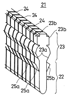
Figs. 2A, 2B and 2C show an insulating
element 21 according to a first embodiment of the
present invention. More particularly, Fig. 2A is a
perspective view of the insulating element 21, Fig. 2B
is a cross-sectional view of the insulating element 21,
and Fig. 2C is a plan view of the insulating element
21.
The insulating element 21 has an insertion
portion 22 and a holding portion 23, these portions
being integrally formed by an insulating member of a
plate shape. It is preferable that the insulating
member used in the present invention is a member which
has insulation performance, incombustibility and
flexibility, and is, for example, nylon. It is
possible to use an insulating material either
incombustibility or flexibility. The insertion portion
22 has an end portion which becomes narrower toward the
tip end thereof. The holding portion 23 has a tapered
portion 23a, which is connected to the boundary of the
insertion portion 22. The cross-section of the tapered
portion 23a becomes wider as the distance from the
above boundary becomes longer. Further, the holding
portion 23 has a projection 23b, which has a shape
facilitating gripping of the holding portion 23 and
slightly projects forward and backward.
A plurality of grooves 24 are formed around
_ 7 _ 21 2789 8
1 the body of the insulating element 21 and are arranged
at predetermined constant intervals in the longitudinal
direction of the insulating element 21. The grooves 24
are used to divide the insulating element 21 into parts
or used to flexibly bend the insulating element 21 so
as to match the shape of a hole formed on a circuit
board such as a printed circuit board.
The insulating member has engagement parts
25a and 25b, which extend upward from the front and
back surfaces of the insertion part 22 and are
separated from each other in the longitudinal direction
by the grooves 24. The engagement parts 25a and 25b
are integrally formed parts of the insertion portions
22 and lower ends pivotably connected to the front and
back surfaces of the insertion part 22. As shown in
Fig. 2B, the distance "a" between the boundary of the
insertion portion 22 and the holding portion 23 and the
top ends of the engagement parts 25a and 25b is
slightly less than the thickness of a circuit board
(31), which will be described later.
Fig. 3 is a perspective view of a printed
circuit board 31 into which the insulating element 21
shown in Figs. 2A, 2B and 2C is inserted. Fig. 4 is an
enlarged perspective view of the insulating element 21
into which the insulating element 21 is inserted into
the printed circuit board 31.
As shown in Fig. 3, a high-voltage area 32
and a low-voltage area 33 are defined on the printed
circuit board 31, which is, for example, provided in an
electric product such as a CRT. In the high-voltage
area 32, there are mounted high-voltage components 34
such as a predetermined number of power transistors
34a, capacitors 34b and resistors 34c. In the low-
voltage area 33, there are mounted low-voltage
components 45 such as a predetermined number of IC
(Integrated Circuit) chips 35a. The components used in
the first embodiment of the present invention are of a
- 8 - 212789 8
-
1 lead insertion type. Lead holds (not shown)
corresponding to the leads of the components are formed
in the printed circuit board 31 and are soldered.
A through hole 37 having a rectangular shape
is formed in an intermediate portion on the printed
circuit board 31 between the high-voltage area 32 and
the low-voltage area 33. The insulating element 21 is
inserted into the rectangular hole 37. The insulating
element 21 shown in Figs. 2A through 2C are cut one of
the grooves 24 so as to match the length of the
rectangular hole 37, and the cut insulating element 21
is inserted into the rectangular hole 37. The holding
portion 23 is located on a parts surface (mounting
surface) 31a of the printed circuit board 31, and the
insertion portion 22 is located on a soldering surface
3lb of the printed circuit board 31. If the hole 37
has a curved shape, the insulating element 21 is bent
at the grooves 24 so as to have the same curved shape
as that of the hole 37.
More particularly, as shown in Fig. 4, when
the insulating element 21 is inserted into the hole 37
of the printed circuit board 31 from the parts surface
31a thereof, the engagement parts 25a and 25b are
closed to come into contact wit the front and back
surfaces of the insertion portion 22. When the
insulating element 21 is completely inserted into the
hole 37, the engagement parts 25a and 25b are opened
and come into contact with the printed circuit board 31
in the vicinity of the hole 37. In this manner, the
insulating element 21 is fixed to the printed circuit
board 31. The tapered portion 23a function to securely
fix the insulating element 21 to the printed circuit
board 31.
The distance between the high-voltage area 32
and the low-voltage area 33 defined on the printed
circuit board 31 is determined by the height of the
insulating element 21 (the height of the insertion
9- 2127898
-
1 portion 22 and the height of the holding portion 23)
used for the printed circuit board 31. In this case,
the insulating element 21 is designed so that at least
the insertion portion 22 is located so as to be higher
than the tip ends of the leads of the high-voltage
component 34 and the low-voltage component 35, and at
least the holding portion 23 is higher than the top
portions of these components.
Fig. 5 is a diagram showing the function of
the insulating element 21. As shown in Fig. 5, the
high-voltage component 34 and the low-voltage component
35 are mounted on the printed circuit board 31. It
will now be assumed that the distance x between the
facing sides of the components 34 and 35 on the parts
surface of the printed ~ircuit board 31 is defined and
the distance y between facing ends of soldering lands
36 on the soldering surface of the printed circuit
board 31 is defined. The distance y is the shortest
distance between the components 34 and 35.
Further, it will assumed that X denotes the
height of the insulating element 21 inserted into the
hole 37 from the parts surface 31a, and Y denotes the
height of the insulating element 21 inserted into the
hole 37 from the soldering surface 31b. The height of
the insulating element 21 is equal to X ~ Y + d in
total where d is the thickness of the printed circuit
board 31.
Hence, the space distance between the high-
voltage component 34 and the low-voltage component 35
q l to (Xl + X2 + X3 + X4 + X5) on the parts
surface 3la and is equal to (Y1 + Y2) on the soldering
surface 31b. It will be noted that the space distances
on the parts surface 31a and the soldering surfaces are
respectively x and y if the insulating element 21 is
not provided. Hence, the insulating element 21
functions to lengthen both the space distances on the
parts surface 31a and the soldering surface 31b.
- 10 _ ~2127898
-
1 According to the first embodiment of the
present invention, the space distance (insulation space
distance) between the high-voltage component 34 and the
low-voltage component 3S defined by the safety
regulations of the standards depends on the height of
the insulating element 21 based on the potential
difference between the components 34 and 35 (in the
case where the surface shape of the insulating element
21 does not affect the space distance).
Fig. 6 shows the relationship among the
height of the insulating element 21, the potential
difference between the high-voltage component 34 and
the low-voltage component 35, and the insulation space
distance. The insulation space distance needed on the
basis of the potential difference between the
components 34 and 35 actually spaced apart from each
other by a distance x of 2 mm (the distance y is also 2
mm) can be obtained by the height X of the insulating
element 21 from the parts surface 31a and the height Y
of the insulating element 21 from the soldering surface
31b.
Turning now to Fig. 5 again, when the
potential difference between the high-voltage component
34 and the low-voltage component 35 spaced apart from
each other by a distance x of 2 mm is 150 [Vrms], the
necessary insulation space distance is equal to or
greater than 4.00 mm. When the height X (Y) of the
insulating element 21 is 2.0 mm, (X1 + X2 + X3 + X4 +
X5) is equal to 4 mm, and (Y1 + Y2) is equal to 4 mm.
As described above, even when the high-
voltage component 34 and the low-voltage component 35
are arranged close to each other, it is possible to
ensure the necessary insulation space distance required
by the safety standards by interposing the insulating
element 21 between the components 34 and 35. That is,
the insulating element 21 functions to substantially
increase the space distance. It will be noted that use
2l27898
1 of the insulating element 21 contributes to down-sizing
of the printed circuit board 31 and thus the electric
products.
In the above-mentioned first embodiment of
the present invention, the components are of the lead
insertion type. However, the insulating element 21 can
be used for components of a surface mounting type in
which leads are soldered on the parts surface of the
printed circuit board.
Fig. 7 is a cross-sectional view of a second
embodiment of the present invention. In Fig. 7, parts
that are the same as those shown in the previously
described figures are given the same reference numbers,
and a description thereof will be omitted. An
insulating element 2la according to the second
embodiment of the present invention has extensions 41a
and 41b horizontally extending from the front and back
surfaces of the holding portion 23. The extensions 41a
and 41b have predetermined lengths (which may be equal
to or different from each other), and are integrally
formed with the other parts of the insulating element
21a.
The extensions 41a and 41b extend above the
high-voltage area 32 and the low-voltage area 33, and
the space distance between the high-voltage component
32 and the low-voltage area 33 is lengthened by the
lengths of the extensions 41a and 41b. Even if the
components 34 and 35 are arranged to close to each
other, it is possible to ensure the insulation space
distance by using the insulating element 21a. It is
necessary to ensure the insulation space distance on
the soldering surface 31b by the length of the
insertion portion 22 of the insulating element 2la.
Hence, the insulating element 21a is effective
particularly to components of the surface mounting
type. In this case, it is possible to reduce the
length of the insertion portion 22.
- 12 _ ^ 2I2 789 8
1 Fig. 8 is a cross-sectional view of an
insulating element 2lb according to a third embodiment
of the present invention. In Fig. 8, parts that are
the same as those shown in the previously described
figures are given the same reference numbers. The
insulating element 21b has only the extension 41b,
which extends above the low-voltage area 33 on the
printed circuit board 33. The extension 41b is
integrally formed with the other parts of the
insulating element 21b. The extension 41b functions to
lengthen the space distance between the high-voltage
component 34 and the low-voltage component 35. The
insulating element 21b is effective to the surface
mounting type components, and particularly to a case
where the high-voltage component 34 radiates a large
amount of heat.
The present invention is not limited to the
specifically disclosed embodiments, and variations and
modifications may be made without departing from the
scope of the present invention.