Note: Descriptions are shown in the official language in which they were submitted.
',~~Q~~,~
1~'~ 93/ 1553 ~ ~'J I J V i J SJ
PCT/~1593/00838
-1-
TAPERED SEMICONDUCTOR LASER GAIN ;
STRUCTUkE WITH CAVITY SPOILING GROOVES
Field of 'the Invention
The invention pertains to semiconductor laser
amplifiers. More particularly, the invention
pertains to semiconductor laser amplifiers having
tapered amplification regions.
Backqround of the Invention
Semiconductor laser oscillators (i.e., laser
light sources, hereinafter lasers) and semiconductor
laser amplifiers (i.e., hereinafter amplifiers) were
first dweveloped in the 1960s. Such laser oscillators
and~a.mpl.iziers~ offered the obviouw.advantag~e of~
extremely small size over the other types of lasers.
(A typical semiconductor amplifier may be on the
order of few hundred micrometers long). These first
semiconductor lasers were fabricated of a single type
of semiconductor.
A modern semiconductor laser oscillator or '
amplifier typically comprises a semiconductor '
heterostructure; that is~, it is made from more than
one semiconductor material such as gallium arsenide
1'
(GaAs) and aluminum gallium arsenide (AlGaP.s).
t
A
.~.,..:-......... . , ..,, -:" ~. .-~~,;..~,........ .. ..,~ .'.. ~...'.'W..,.
~: ~;.'.:, ,.'. ;...; .,:.' ' ;'.'
.,
t.'-:
WO 93115537 1 ~ , , 1'CT/US93/U0838 ; ; ;
~~E~~'~~~ 2
A modern semiconductor laser oscillator or
amplifier typically comprises a semiconductor
heterostructure, that is, it is made from more than
one semiconductor material such as gallium arsenide
(GaAs) and aluminum gallium arsenide (AlGaAs).
Semiconductor oscillators and amplifiers are made
from a combination of semiconductor materials which
have different bandgap energies in order to achieve
electrical current confinement as well as different
optical indices of refraction in order to achieve
optical confinement.
An exe:nplarv double heterostructure amplifier 10
of the prior art is illustrated in rIGS. 1 and 2 and
comprises three layers of~semiconductor material; 1)
a p-type material 12 with a relatively high bandgap,
such as AlGaAs, 2) an n-type material 14 with
relatively high bandgap, which may also be AlGaAs,
and 3) a relatively low bandgap p-type material 16,
such as GaAs, sandwiched between the other two
layers. A metal contact 1~ is placed in contact with
the top surface of the top layer, which may be either
the n-type or p-type high bandgap material. When
sufficient current is passed through the metal
contact, electrons and holes are injected into the
active region lc from the high bandgap material
layers 12 and 14. These electrons and holes are
trapped in the potential well created by the low band
gap GaAs'material. Since the electrons are trapped
i.
i;
a
t
, .
SLJBST'iT~:ITE SHEET
. . : v ~ .
l..
' ~~i
_ WO 93/1553'1 PCT/US93/00838
I
'on 16 the are forced to combine
in the active regl , y f
with each other in the GaAs material . Light ~ i
introduced into this region will be amplified.
Confinement of the light to the GaAs layer 16 is
provided by the wave guide properties of the
AlGaAs/GaAs/AlGaAs mat erial structure. The AlGaAs
layers have a lower optical index of refraction than
that of the GaAs material thus providing total
internal reflection of light off of the junctions 13
and 15 so that the light remains within the GaAs
layer 16. The electrical contact 18 defines the
lateral boundaries 17 and 19 of the amplification
region.
Many approaches have been proposed to achieve the
goal of high-powered, continuous-wave operation with
a single-lobed spatial mode output from semiconductor
lasers or semiconductor amplifiers. One such
approach is to employ a laterally tapered electrical
contact 18 so as to define a laterally tapered
amplification region such as is illustrated by FIG. 1.
In operation, light generated by a laser 11 is
focused by a lens 21 on the input facet 20 of tapered
amplifier 10. The use of a tapered amplification
region allows for greater gain before saturation than
non-tapered amplifier structures because it permits a
single-spatial-mode beam entering at the input facet
17 to expand with. nearly free diffraction as it
propagates through the isemiconductor. If the beam is
L :..:
!.
a
SU~~TiTUTE SHEET
::..:..
WO 93/15537 , PCT/US93/On.R38
r:~~ dU ~~~~ ' - 4 w.~
allowed to spread naturally without any external
interference, the beam will spread in its lowest
Gaussian mode, thus leading to the desired. spatially
uniform amplified output beam. Also, si:.ce tr.e beam
expands as it increases in Bower, gain saturation is
reduced. Further, the expansion of the beam reduces
the possibility of optical damage at the output facet
22 because the power in the beam is more spread out.
The tapered amplification region structure,
however, has a drawback in that such a structure i.s
easily susceptible to self-oscillation.
Self-oscillation occurs when a small portion of the
light striking the output facet is reflected back
into the semiconductor medium. The reflected light
interferes with the input light as it propagates down
the semiconductor causing non-uniformity in the gain
profile as well as in the spatial distribution of the
output light and possibly even temporal instability
of the output light.
In semiconductor lasers, well defined and
controlled self-oscillation is desirable and, in
fact, necessary in order to achieve losing. However,
uncontrolled self-oscillation is unnecessary and
therefore undesirable. Further, in semiconductor
amplifiers, any self-oscillation is unnecessary and
therefore undesirable since it interferes with the
input light and causes the generation of higher order
spatial distribution modes (i.e.. mode conversion)
~UB$T1TUTE SHEET
WO 93/15537 - ~ '~ ~ ~ ,;; ~.~ h~ r~ PCT/US93/00838
S ' ' f
leading to non-uniformity in the spatial distribution
of the beam. Tt also reduces gain. Self-oscillation
can also lead to temporal instability of the output
beam.
This problem can be partially alleviated by using
anti-reflection coatings on the input and output
facets 17 and 22. However, this solution is ofte.~.
difficult.to achieve in practice and, in fact, may be
impossible to incorporate in certair. monolithic
implementations where a semiconductor master
oscillator laser and a semiconductor amplifier are
integrated on the same chip.
Accordingly, it is an object of the grese.~.t
invention to provide an improved semiconductor laser
amplifier.
It is a further object of the present invention
to provide a tapered semiconductor amplifier with
increased ability to suppress self-oscillation.
It is another object of the present invention to
provide an improved tapered semiconductor laser
amplifier with improved ability to suppress mode
conversion.
It is yet another object of the present invention
to provide an improved semiconductor laser oscillator.
It is one more object of the present invention to
provide a semiconductor gain structure that can be
used as a laser oscillator or as a laser amplifier
depending~~on the application of anti-reflection
S
coating to the input facet of the structure.
Y.
3
l
l
l
1
Sl,~~ST1TUTE SHEET
.r v:... ~ : : . ' . v . . .. : .. :. . . . "- : . . , ., . ' ; ,
T
t...a., ..
w : ,.
WO 93!15537 , ~ ~ ~ ~ ~ ~~ J~ - 6 - PCT/US93/øfi.R38
..~ i
Summarv of the Invention
The invention comprises a tapered semiconductor
gain structure which can be utilized as a
semiconductor laser amplifier or a semiconductor
laser oscillator.
The invention comprises a semiconductor gain
structure employing a tapered gain region between
cleared input and output facets. The lateral
dimension of the gain region of the semiconductor is
defined by a tapered electrical metal contact or. the
surface of the semiconductor. A wave guiding layer
is constructed by conventional layering of
semiconductor materials. Light of a fundamental
Gaussian spatial distribution mode which is focused
onto the input facet adjacent the 3ain regian
propagates freely down the tapered gain region
expanding in its fundamental Gaussian mode and
gaining in power. There is no intentionally imposed
refraction index gradient at the boundary of the gain
region. The gain region is defined solely by the
electrical contact. Accordingly, the amount of light
reaching the gain structure boundary which is
reflected back into the gain structure is minimized,
thereby reducing interference between reflected light
and the amplified input light and generation of
higher order spatial distribution modes.
Further, two reflective cavity spoiling grooves
are etched in the semiconductpr adjacent the input
,.
!':
SU~STiTUTE SHEET
s:
:..
~~._
PCTI US93100838 ~ ~_ ,
WO X3/15537 _ .~
.:
n
a
facet with a gap provided therebetween so that. the
i
inDUt light can pass through and propagate do~.fm the '.,
_ ;
gain region of the semiconductor. '~'he grooves are
positioned so as to receive the majcrity of light ',
which reflects off of the outaut facet back into t:~e
semiconductor and are angled to reflect that bight
away from the gain region and primarily into the
substrate or the saw-cut lateral edges. accordingly,
undesirable self-oscillation is significantly .educed
ince the majority of the light which is reflected
back from the output facet is directed by the etc:zed
grooves away from the gain region.
~Ihen the~device is used as a laser amplifier.
both the input and output facets are anti-reflection
coated.
However, when the device is used as a laser
oscillator, only the output facet is anti-reflection
coated. Thus, a relatively large portion of the
1 fight which is ref lected off of the center of the
output facet back towards the input facet between the
cavity spoiling grooves is again reflected back into
the semiconductor cavity resulting in oscillation.
The light reflected off of the non-central part of
the output facet is not returned to the input facet,
but strikes the spoiling grooves and is directed
thereby away from the gain region. By virtue of
oscillating only,the light striking the centermost ,
portion of the output facet, oscillation of higher
order spatial distribution modes is suppressed. 1
1
f
S8J~~'TiTUTE ~at-iEET
t
~~.:.
1: r,:-'.
[.;:...
PCT/US93/On838 ; .
W0 93/ 15537 ~ ~ ~ ~ ~ ~ l~ ~ 8 - ,
Brief Description of the Drawings
FIG. 1 is a plan view of a tapered gain structure L
laser amplifier of the prior art.
FIG. 2 is a cross-sectional view taken along ;ine
A-~ of FIG. 1.
FIG. 3 is a plan view of the semiconductor gain
structure of the present invention configured as a
laser amplifier.
FIG.~4 is a cross-sectional view taken along line
A-A of FIG. 3.
FIG. 5 is a plan view of a second embodiment of
the semiconductor structure of the present invention
configured as a laser oscillator.
FIG. 6 is an illustration of exemplary light
distributions of light traveling in the laser
oscillator of FIG. 5.
Detailed Description of the Invention
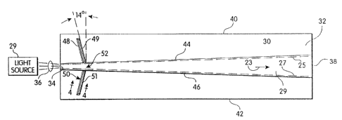
FIG. 3 is a plan view of the semiconductor laser
amplifier of the present invention. FIG. 4 is a
cross-sectional view taken along line A-A of FIG. 3.
The semiconductor layer structure is somewhat
conventional for heterostructure semiconductor lasers
and amplifiers in that it comprises a layer of low
bandg,ap material sandwiched between two layers of .
oppositely doped high bandgap material. A tapered
SU~STiTUTE ~HE~T'
:-~ .... , . ... ~- .
,:,.:;:;
y
CT/1US93/00838
~ ~ ~ ~
) ~~ !~
WO 93/15537
_ g _
,
electrically conductive contact 30 is placed on the 1
surface 32 of the semiconductor structure. Contact
30 may be metal. Light from a laser light source 29 i-
is introduced to cleaved input facet 34 *-r.roucrh
focusing lens 36. The degree of taper is selected so
as to allow the input beam to spread naturally ~n its
fundamental Gaussian spatial mode such that its light
intensity profile has no nulls when it reaches the
cleaved output facet 38. The lateral edges 40 and 42
of the semiconductor are saw-cut. No intentional
gradiA_~.t in the index of refraction of the marer~a~.
is imposed at the boundaries 44 and 46 of the gaib:
region. The boundaries 44 and 46 are defined solely
by conductive metal contact 30. Reflective cavity
spoiling grooves 48 and 50 are etched through the
waveguide layer at positions selected to receive
light reflected off of the autput facet 38 before it
is returned to the input facet 34. The grooves are
etched at an angle such that they reflect the light
away from the gain region. A gap 52 is provided
between the grooves 48 and 50 to allow the input
light to propagate between the grooves down the gain
region. In the preferred embodiment, the grooves are
angled at i4 from the plane para1121 to the output
facet 38 and 45 Pram the plane of the waveguide
layer as shown in FIG. 4.
When the gain structure is utilized as an
amplifier, both the input facet 34 and the output
:;.
~.
i
S~BSTITU'~'E ~HEF.T
~.il~ ,
t:.:
WO 93/15537 PCT/US93/00838
~ 1 ~ e~ ~.~ ~l'-~ - m -
facet 38 are coated with an anti-reflection coating
so as to minimize reflection off of these cleaved
surfaces. Nevertheless, Some 'fight is reflected off
of the output facet 38 and returned into the
semiconductor towards the input facet 34. The
majority of such light will strike the cavity
spoiling grooves 48 and 50 whereupon it will be
reflected off of the etched grooves either towards
the saw-cut edges 40 and 42 and out of the
semiconductor or down into the substrate (not
shown). The small amount of light which passes
through the gap 52 between the grooves strikes the
input facet which is also coated with an
anti-reflective coating. Accordingly, since the
majority of light reflected off of output facet 38
strikes the cavity spoiling grooves, the amount of
light which can oscillate within the semiconductor is
significantly reduced.
By having the smallest possible index gradient at,
the boundaries 44 and 48 of the gain region,
excitation of high-order index-guided modes is
substantially eliminated. Such modes would tend to
be dispersive and to create extra phase variations
across the beam. The spatial beam quality would, in
turn, be deteriorated.
However, since there is no intentionally imposed
refractive index gradient at the boundaries, most of
the light which strikes the boundary simply passes
3'
aI.JBST1TUTE :SHEET
WO 93/15537 ~ ~ n ~ PCT1L~93/00838
11 ~~~..U~1~~ ' 1.
Through it rather than being reflected back into the
gain region. a small amount of index guiding may be !
r.
unavoidable due to thermal effects caused by the
1
current flowing through the contact patch 30 as wei
as gain saturation effects and strain effects.
Nevertheless, these effects would on~.y cause a sma~'_
fraction of the output power to fall outside of the
main spatial mode.
The gain structure disclosed herein may also be
modified for use as a laser oscillator, i.e., a laser
light source. FIG. S is a plan view of the gain
structure of the present invention modified to
achieve a controlled self-oscillation in the
fundamental Gaussian spatial mode so as to achieve
lasing action. In FIG. 5, like features are
indicated with the same reference numerals as in
FIG. 3. The structure is essentially identical to
the FIG. 3 embodiment except that input facet 56 is
not coated with an anti-reflection coating.
Accordingly, a significantly greater portion of the '
light reflected off of the output facet which is
returned between the cavity spoiling grooves to the
input facet 56 is reflected back into the
semiconductor. Accordingly, a significantly large
amount of self-oscillation is allowed so that lasing
may occur.
The employment of the etched grooves in this
configuration as ,an oscillator leads to an~extremely
stable fundamental Gaussian oscillation. As
s
1 ,.
i
r
i .
3
SLJ~STiTUTE SHEET
,.
WO 93/15537 c3 A c~ ~ %~ ~ PCT1U593/0,~'.R38
~.~~UE~~i - 12 -
previously explained, the majority of the light which
is reflected off of the output facet strikes vhe
etched grooves and is directed out of the
semiconductor. Only the poxtion of the iigrt which
strikes the output facet very close to its center, as
'lustrated at 38a in FIG. 5, can pass through she
gap 52 between the etched grooves 48 and 50 and
strike the input facet 56. As illustrated in ~iG. 6,
the vast majority of light which strikes the center
38a of the output facet 38 is very uniform in
intensity thus leading to superior suppression of
high order spatial distribution modes. Curve 60 i.~.
FIG. 6 illustrates an exemplary spatial light
intensity distribution of light propagating in the ; '
gain region in the fundamental Gaussian mode. Dashed
curve 62 and dotted curve 64 illustrate the spatial
light intensity distribution of light propagating in
the gain region in the second and third harmonics of
the fundamental. The relative intensities of the
various harmonics are not accurate. As previously
discussed, the present invention substantially
reduces generation of higher order spatial modes.
However, the second and third order harmonics are
shown enlarged for ease of illustration. As can be
seen by the juxtaposition of curve 6o with the center
l
portion 38a of the output facet 38, an extremely flat
portion of the light intensity distribution curve of
the fundamental harmonic 60 strikes the output facet
l .
~
n ,
x...
g
I
s
SUBSTITUTE S~-iEE'T'
1 ,,
'; ,:. :: . , . . . ; ;: .
WO 93/ 15537 ~ 13 ' ~ ~ ~ ~ f? ~ ~~ FCT/U~93/00838
t
the center region 38a (i.e., the portion which will ;
be returned to input facet 56 for oscillation). Lt
can also be seen with respect to the second and third ,
s
harmonics shown by curves 62 and 64 that the light
intensity distribution in region 38a is not as
uniform as curve 60 and is of much lower power t:~an
curve 30. Accordingly, higher spatial mode .
suppression is achieved for two primary reasons. '
First, a much lower amount of light energy in the
higher harmonics is returned to the input facet 56.
Second, the light of the fundamental Gaussian spatial
mode which is returned to the input facet .is
extremely uniform in intensity because the (latest ~,
portion of the light distribution curve strikes
region 38a of the output facet 38. Accordingly,
oscillation of light of extremely uniform light
distribution occurs thus leading to superior
suppression of high order distribution harmonics.
The gain structure disclosed herein was
implemented as a laser amplifier. Total continuous
wave output power in excess of I.2 watts with 1.0 -
watts contained in a single-lobed spatial mode was
achieved.
In this implementation, the reflective cavity
spoiling grooves were fabricated by a reactive ion
etching (RIE) process with the use of an oxide etch
mask. The RTE system was. operated at 28 mTorr ~
pressure with a H2:CH4 plasma established by a
4:1 gas-flow ratio and an rf power of 0.9
:~
,:
f
SUBSTITUTE SHEET
~,;;, v.
~y;.::
WO 93/15537 F'C'T/US93/0(~838
14 _ y=..
watts/cm2. The wafer was then coated with 300 nm
of Si02. The linearly tapered contact pad was
formed using photolithography to open the tapered
pattern in the oxide. Metals (Ti/Au) were evaporated
over the entire waver making ohmic contact to ~he
tapered region. The semiconductor amplifier was
fabricated from Ir.GaAs/AIGaAs graded-index
separate-confinement heterostructure
single--quantum-well semiconductor material. This
type of strained-layer quantum well material has been
shown to be inherently more reliable than
conventional unstrained GaAlAs material. The device
was 2 mm long and 2.00 um wide at the broadest part
of the taper. The input and output facets were
cleaved and anti-reflection coated with a
quarter-wave layer of SiOx, where x is adjusted to
give an index near 1.8, with a residual reflectivity
estimated to be approximately lo. The wavelength of
operation for this embodiment was 970 nm.
The invention may also be implemented utilizing
back-biased junctions instead of the etched grooves.
The back-biased junctions form absorbing regions that
are difficult to optically saturate. It may also be
possible to use other spoilers, such as long regions
of proton-bombarded material or other absorbing
schemes, and other techniques to deflect the beam out
of the cavity.
SUBSTITUTE SHEET
': ': :., .. . ~, :,. , ; _ _;
;..Y x,.
WO 93/15537 - 1 S - ~ ~ t~ ~ ',' ~ ,!~ PCT/US93/00838
l
Using the inventive gain structure disclosed ~ !
1
herein as, a high power unstable oscillating laser '
rather ~han an amplifier by applying the
anti-reflection coating only to the output facet, an
output power of 1.5 watts continuous has been
achieved with far-field intensity distribution
superior to that of high-power laser arrays which
operate i~ the out-of-phase mode.
The inventive gain structure disclosed herein has
wide applications. Depending on the composition of
the strained layer semiconductor material, the
amplifiers can be made to operate at wavelengths
ranging from 0.8 to 1.0 um. Accordingly, the
present invention can be used as an amplifier or as
an unstable oscillator suitable far pumping
rare-earth doped fiber amplifiers where high-spatial
mode quality is required. In addition, these devices
can be used in other pumping applications such as
solid-state laser pumps, and particularly as end
pumps. Since high spectral purity and high
modulation rates can be achieved by controlling the
master oscillator characteristics, these amplifiers
can be used to build high-powered transmitters for
free-space optical communication systems.
High-powered defraction-limited diode source
applications are also possible for efficient
frequency-doubling in t~e,blue-green region of the
3
spectrumlfor optical-disk-memory and other
3
applications.
,.
SU~STiTUI'E ~HEE'T'
,,:
WO 93/15537 PCT/US93/0~838 ~,
a3~~~ - 16 -
Having thus described a few particular
M I
embodiments of the invention, various alterations, .
modifications and improvements will readily occur to 1,
those skilled in the art. Such alterations,
modifications and improvements as are made obvious by
this disclosure are intended to be part of this
description though not expressly stated herein, and
are inter.~.ed to be within the spirit and scope of the
invention. Accordingly, the foregoing descript:.on is
by way of example only, and not limiting. The
invention is limited only as defined in the following
claims and equivalents thereto.
What is claimed is:
<:
.:
~u~~1~E ~HE~
. . , .,, . _ , . .. ,._. .... .,,. ; , , -, ~ v ,