Note: Descriptions are shown in the official language in which they were submitted.
': . .~ ' ' -
~WO93/16574 212 8 210 PCT/US93/014~
HIGH DENSITY CONDUCTIVE NETWOR~S ~. ;-
AND METHOD AND APPARATUS FOR~RING SAME
: ,. .: . ~. :'
.,, -. ,
This invention generally relates to supported
conductive networks (SCN), flexible or rigid, and their
manufacture. In particular, this invention relates to
such conductive networks which have densely packed
conductive paths (HDSCN), and to a method and apparatus ;
for making the conductive networks. . ::
Backqround ~f~the Invention .:
Developments in the electronics industry require the
use of more densely pac~ed electrical modules and ;~
circuits, each requiring multiple interconnections to one ,;:
another. However, there is a practical limit to the ~ .
15 density that can be achieved using conventional connective ::~
network:s. Tn a typical present day application, a floppy
disk drive may require a connection to a rec~rding head
whose c:onductors are only on the order:of 0.2 mm (0.008
inches) on center and associated 3umper conductors must
have a similar spacing. Further, recent liquid crystaI
displays have conductors which are even more closely .
packed, for example, 0.1 mm (0.004 inches) on center, with
similar requirements for interconnection conductors. In ~ .
addition, there is growing use of cera~ic PC boards to ~ .
accommodate multiple IC chip arrays which aIso require
h gh~density connectors and custom interconnect cables for
: purposes of ter~inating those co~ponents.
As a direct resultlof the growth iD the circuitlboarjd
ndustry, there has been a parallel increase in the volume
of en~iro~mentally-hazardous chemicals generated by the
oonventional etching and deposition processes. For
: example,: it is not unco~mon for one circuit board
fabrication facility to generate ~,000 litres (1,000 U.S.
:. ~ .",,:
': ' ' .~.: ., ;.
:. ::: . : .:
: .: .:, .;:.
W093/1~74 PCT/US93/01! ~.
2~28210
-2-
gallons) per day of photo resist stripper and 4,800 litres
(1,200 U.S. gallons) per week of developer solution.
These toxic: wastes must be transported off-site for proper
disposal at hazardous waste management sites. Thus, there
is an urgent need for a non-chemical method for the
manufacture of conductive networks.
It is an object of this invention to provide a
relatively inexpensive, high-quality, densely packed,
supported conductive network for use in fabricating rigid
or flexible circuit boards, that can be built without the
use or generation of environmentally hazardous chemicals.
Another object of the invention is to provide a
flexible conductive network having conductive paths which
are profiled to self-align with corresponding conductors
of other conductive networks.
Yet another object of the invention is to provide
methods of making conductive networks having one or more
of the~above advantages.
$u.mmarY of the Invention ~
20Simply stated the present invention relies on one
basic principle, namely, the creating of a cirCuit pattern
in a planar sheet of conductive material by displacing
waste material into a plane whsre it can be easily removed
and then mechanically removing the waste material.
25Generally, in this invention, a flexible conductive
network is made by shaping an electrically conductive
sh-et of material (for example, a copper lamina or a
~: ~ laminate of such materials with~or without plated on, or
inlaid, contact points) to form a desired conductor
~pattern on the sheet. A fo~ming process forms ridges and
troughs of desired cross-sections in the sheet with one of
these corresponding to a conductor pattern~ Usually a
dielectric substrate is then attached or formed to one
'"~ '. ''~'.'
;' ~--'.;'~,',
!WO 93~16574 212 ~ PCT/US93/014~ ~-~
-3- -~
side of the sheet, for example, with an adhe~ive filling
the spaces between the substrate and the sheet.
Alternatively, the dielectric su~strate may, in
appropriate circumstances form a laminate with the
conducti~e sheet prior to the formation of the ridges and
troughs.
Next, the exposed metal face of the metal-dielectric ~ ~
lamination is exposed to a removal process, for example
precision milling or grinding to cut away a pre-determined
amount of the material to isolate the adjacent conductors
of the pattern from one another which thereupon may, if
desired, constitute channeled conductive paths attached to
the d:ielectric substrate, each of which has a desired
cross-section or profile.
15This process offers significant advantages over the -~
conve~tional imaging and etching or additive (plating-up) ~ ~ ;
techniques normally used to ~ake printed circuit
conductive networks. It significantly reduces labor costs
and produces impro~ed yields. It also allows the use of
metal sheetæ or foils with minor inclusions which cannot
be us~d in a process involving etching becau~e it would
resu~t in non-uni~orm etch rates. Further, in the process
of this invention, the throughput is th~ same for circuits
who~e metal foils have different thicknesses. This
contrasts to the usual imaging-etching process wherein the
li~e speed is directly proportional to the foil weight
because it takes longer to etch thick foil than thin foil.
The pr~cess of this invention results in additional
savings because it is a~dry process which does not entail
the added expenses related to ancillary processing of
hazardous materials and chemical disposal.
According to the invention there is provided a method ~-
for manufacturing a supported conductive network
: . .
. . .
WO93/16574 PCT/US93/01~
% ~ ~4~ ~ :
comprising the st ps of a) forming a planar electrically .
conductive sheet into a non-planar pattern ha~ing a
dielectric material fast with a first face thereof; and
b) removing portions of the sheet from a second face ~
5 thereof to form electrically insulated electrically ~-
conductive paths supported by the dielectric material.
Also according to the invention there is provided a
supported conductive ne~work having self-aligning :~
electrically conductive paths comprising a dielectric
layer; and an electrically conductive layer supporte~ by
said dielectric layer; said metallic layer being formed
into conductive paths electrically in~ulated from one
another, and said conductive paths having outwardly
inclined side walls for aiding in aligning said conductive
15 network with conductive contacts of a connecting member. ;~
Also according to the invention there is provided an
apparatus for manufacturing a flexible conductive network ~.
comprising neans for forming a planar electrically .. ~
conductive sheet into a non-planar pattern with a flexible ~-.
20 dielectric material fast to a first face of said sheet and :~:
me~ns for removing portions of said metallic sheet from a . .
second face of said sheet to form electrically insulated
electrically conductive paths.
The inventive process will yield a rigid circuit
(SCN) board or flexibIe circuit capable:of precisely
aligning with and ~aintaining Gontact with the conductors
of a surface ~ounted device. Typically these devices have :
conductors located 0.3l ~m (0~012 inches) on center or
less. This precise alignment is primarily due to the ;`
interlocking characteristic of the shaped conductor.
Conductors and their ter~inating points can, by using
the present. invention, be designed to any specific ~;
.~093/16574 2 ~ ~ ~ 2 ~ ~ PCT/US93/014~
electrical parameter or configuration and may be randomly :~
located on any non-conductive base material. -
The inventive process also has the adYantage of
running an SCN production line capable of processing many
diff~rent conductiYe materials such as brass, copper,
aluminum etc., without fear of chemical contamination of
costly chemistry change-over, common with conventional
etching systems. :: -
The following is intended to summarize the
10 versatility and technical advantages of the inventive ~ ~.
(DryFlex) process~
a) The Dryflex process is equally effective on high ~ :
volume and intermediate volume jobs;
b) once the electrical and mechanical
characteristics of a circuit are established and built
: into the hardened steel te~plate, there is circuit
- repeatability;
c) Conductors can be plated with any sur~a~e
finish;; .
20d) Base laminate may be ~us~d (melted) to the `~
formed conductive sheet eliminating the need ~or an
adhesive (This an only be accomplished, without causing ~;
conductor distortion (swim), using the ~ryflex process);
e) The Dryflex process eliminates common yield .
problems associated with con~entional etched cîrcuits such
as,: artwork distortion, dirt or dust, scratched resist, ;~
inconsistent etching chemistry, etc;
~ f) The Dryflex; process offers a signi$icant
: ~ ~ reduction in direct labor; :
30 g) The Dryflex process eliminates chemical .:
processing materials and related disposal expanses; -
WO93/16574 PCT/US93/01' `
~8~ 6- ~
- h) The ability to produce conventional copper
circuit for less than l/2 of direct manu~acturing costs
using etching techniques;
i) The ability to manufacture low cost, channelled
5 conductors insulated with any flexible or rigid insulating ::
material;
j) The ability to manufacture low cost, channelled .
conductors insulated and mounted to a second SCN and/or to
a support spring or component stiffenex; and : .
k) The DryFlex process can be used to make high~
density contact clusters for connector assemblies.
Brief Descri~tion of the Drawin~s .
The invention will now be described~ by way of
example~, with reference to the accompanying drawings, in
which~
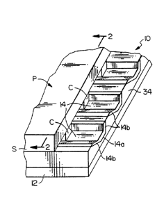
Fi.g. 1 is a fragmentary axonometric view of a self~
alignimg conductive network (SCN) made in accordance with
the invention and shown coupled to a printed circuit;
Fi.g. 2 is a sectional ~iew taken aIong lines 2-2 of
Fig. l;
Figs. 3 and 4 are views similar to Fig. l showing
successive steps involved in making the conductive network
of Fig. l;
Figs. 5 and 6 are s~ctional views taken along lines .
5-5 and:6-6 of Figs. 3 and 4, respectively;
: ~ Fig.~ 7 is a cross-sectional view of a portion o~ a
: conductive network in which the side walls have been
removed;
~ Fig. 8 is a diagram~atic view illustrating apparatus ;~
~for use in the manufacture of circuits networks of the
present invention;
IWO93/16574 2 ~ 2 ~ 2 ~ ~ PST/US93/01454
-7~
Fig. 9 is a sectional view, similar to that of Fig.
6 with conductors isolated and with a spring backing layer
attached for use in connector assemblies;
Figs. lo and 11 are perspective and top views
respectively illustrating the use of the conductive
n~twork for holding a reservoir of solder; .
Figs. 12 and 13 are sectional views illustrating a
cold pressure fusing operation; ~ :
Figs 14 and 15 are, respectively, sectional views of . ~
10 the components of and the assembled construction of a ~.
conductive network according to the present invention
incorporating stress hardened pads and a shield; and
Figs. 16 to 19 illustrate the process for making an
SCN according to a further embodiment of the invention.
Detailed Desc~iption of Preferred Embodiments of the
Inventi~pn ~ : ', ,- ' ~. ~-'',-
Referring to Figs. 1 and 2, a flexible conductive .
~etwork incorporating the invention is~shown generally at
10. The network has a dielectric substrate 12 which .`.
carries a densely packed cluster of self-aligning
conductive paths 14. Conductive network 10 is shown ;.
coupled to a more or less conventional conducti~e network .~
(for example,.printed circuit P) ccmposed of a substrate `~:
S which supports a set of printed conductive paths or . .. ..-~.
25 conductors C which are arranged to interfit and interlock .
: :~ with the conductive paths 14 of conductive networ~ 10.
: :~ The~ :tWQ ~ illustrated networks are connected electrically ~ ~
and~mechanical by clamping the~ together by a suitable .. ~ ~.
~: cla~p shown in: phantom at M in Fig. 2. Each conductive
3~: path 14~has a bottom wall 14a and a pair of spaced-apart
inclined;side walls 14b so that:the cross-section of each : .
conductive path ~4 is trough-like. The bottom wall 14a is ~-~
generally recessed fro~ about 0.025 mm (0.001 inches) to .. :~
WO93/16574 PCT/US93/01~ `
Q
-8~
about 0.125 mm (0.005 inches) below the surface of the
conductive network. Due to the special profile or cross~
sectional shape of the conductive paths 14, conductive ;
paths 14 interfit or interlock with the corresponding
conductors C of circuit P so as to maintain the conductors
of the two networks in perfect alignment. The conductive
network 10 is best suited for precisely aligning and b
maintaining contact with conductors which are less than
about 3.8 mm (0.15 inches~, and preferably less than 0.6
mm (0.025 inches), on center. There is no bridging of
adjacent conduc~ors despite their close proximity.
The inclined sides 14b of conductive paths 14 guide ;~
the corresponding conductors C into proper alignment with
conduc1:ive network lO and proYide wiping interconnections
between the conductors of the two networks. (It is
important to note that the conductive network 10 can be
used on either the female contact or the male pin of an
inter~onnection). The trough-like conductive paths 14
also prevent conductor discontinuity under vibration and
make high-density connections between the two conductive
networks (for example, 10 and P) possible within an -~
established footprint. Nste that by adding additional
adhesive 34 compliance between t~e two networks can be
enha~ced.
25Although conductive paths 14 depicted in Figs 1 and
2 are shown as being straight and~parallel to one another
in a closely packed cluster, the condurtive paths may have
various ~patterns and follow ! different paths along
substrate 12, or interconnect, depending upon the
partic~lar network application, by appropriately
controllin~ the forming operation described below. -~
. . .
R~ferring now to Figs 3 and 5, according to one
embodiment of the in~ention, to make a flexible conductive
' :~
W093/16574 2 1 2 ~ 2 1 ~ P~T/US93/014
_9~
network 10, a planar metallic material 22 (for example,
copper sheet or foil) of a suitable thickness, for
example, about 0.035 mm (0.0014 inches), is cleaned and ~ .
precisely fed between a pair of coining dies, ~hown in
phantom at D in Fig. 5, which coin or emboss foil 22 to
form a non-planar pattern characterized by a set of ridges
24 on one side of the sheet and a corresponding set of
troughs or channels 26 in the opposite side of the she~t.
Typically, the depth of each trough is from about 0.038 mm
(0.0015 inches) to about 0.013 mm (0.005 inches).
Although the ridges 24 in Figs. 3 and 5 are shown as
having a rectangular cross-section or profile, the dies D ;
can be designed to provide ridges of any desired cross~
section~ll shape (for example, hemispherical, ovular, V-
shaped, etc). The coining process not only shapes the
metallic sheet 22, but also stress-hardens it to prepare ;:
the metallic sheet for the lamination step described
below. Thin metallic sheets may require the structural
support of the forming die during lamination.
As shown in Figs. 4 and 6, the flexible dielectric
material 12, for example, 0.025 mm ~0.001 inchj. thick
Kapton sheet, can be laminated to metallic sheet 22 during -.: .
the forming process. The lamination process can also ta~e
place after the for~ing process. In the illustrated : :
laminating process, an adhesive material 34 is adhered to
one side of dielectric material 12 and the dielectric
material is pressed against the side of metallic sheet 22 :
having the ridges 24,~the appropriate hea~ and pressure is
::~applied for the prescri~ed amount of time causing the
~adhesive material 34 to flow and fill the spaces between
the ridges as ~est seen in Fig. 6. Suitable adhesive
materials include, but are not limited to, epoxies,
palyesters and other application specific adhesives.
WO93/16574 PCT/US93/01
C2~ -10~
~lternatively, the flexible dielectric material may be
fused tfor Pxample, melted) to the metallic sheet, thereby
eliminating the need for an adhesive.
The laminate shown in Fig. 6 is then subjected to a -~
5 precision metal removal~process (MRP) which mechanically ~
removes a predetermined quantity of unwanted metallic ~ -
material from the exposed metal side of the laminate (for
example, the material below the dashed line L in Fig. 6)
sufficient to form electrically insulated conductive
paths. As a result of the MRP step, there is formed the
pattern of profiled conductive paths 14 of conductive
network 10 depicted in Figs. 1 and 2. The conductive ~ ;
paths may then be cleaned and plated with a desired finish
coating (for example, gold, lead, or tin) to complete
conductive network 10. The conductive paths may be, for
example, 0.3 mm (O.012 inches) on center. ~ ~-
Also, in accordance with the invention, by changing
the substrate or base materials so that they are rigid
rather than flexible, a printed circuit board having
channeled or "flat" conductors (as described herein) can
be easily constructed in accordance with the preferred
particular embodiments of the invention. In this
embodiment, the dielectric material would be a rigid
dielectric. In other respects, the construction of the
rigid circuit b~ard corresponds to the construction of the
flexible circuitry as illustrated herein. Accordingly,
while the discussion which follows is generally related to
flexible çonductive circuits, the principles of the
circuit manufacturing processes are equally adaptable to
rigid circuit boards~
The conductive paths and their terminating points can
be designed to any specific electrical parameter (for
example, power and signal1 or configuration. For example, --
, ~, .
. . ."' .", . '
;: ., ~:.- ~::-
WO93/16574 212 8 2 ~ ~ PCT/US93/01454
the controlled impedance of each conductive path can be
selected to suit a particular application by appropriately ~-
controlling its configuration and/or its relationship to
an electrically conductive support s~ructure (for example,
a spring layer 58 or shield) if any. It is important to
note that although conductors and/or their terminating
points can be plated with any surface finish, if a
conductor pattern is not electrically connected to a
common plating bus, the gold, by example, must be plated
on ~efore the conductive paths are electrically isolated.
Further, depending on the use of the conductive
network, the conductive paths can be insulated with a pre~
windoweld protective overlay or solder mask. Suitable
insulating materials include but are not limited to,
Kapton, ~ylar and Teflon. This protective overlay
provides a means to construct multi-layer conductive
networks ~for example, multi-layer circuit boards) or to
add shielding material to the conductive network.
In some applications, the channeled conductor~ may
not be required. For example, in building a flexible
printed circuit requiring extreme flexibility, th~ side
wall, despite its thinness, acts to re~uce flexibility.
In this construction, therefore, channelled conductors are
a significant disadvantage. Accordingly, referring to
Figure 7, the method for removing the unwanted metallic
material, for example the use of a precision diamond
tipped ~flywheel cutter, is continued until the desired
thickness of conductor 66a has been achieved. Therefore,
referring to Figure 7, a conductor configuration lacking
the side walls in accordance with other embodiments of the
invention but retaining the advantages of a chemically
free, en~ironmentally safe manufactuxing process and the
. :~
WO93/16574 PCT/US93~01~ i ~
2~ 12~
other advantages of the proce s, results in a structure
66b having significant advan~ages, and low cost~
Unlike some conventional techniques for fabricating
conductive networks (for example, etching and deposition),
the prscess of this invention does not use etchant,
environmentally-hazardous resist, stripper, and developer
solutions. Thus, the expense and environmental hazards
associated with having the resist, stripper and developer
waste solutions transported to toxic waste management
sites is eliminated. Further, the process of this
invention eliminates common yield problems associated with
conventional etched circuits, such as: art work
distortion, scratched or bad acid resistant ink,
inconsistent etching caused by dirt or dust, and
questiorlable etching chemistry. Thus, the use of this
process will clearly result in a reduction in labor costs
and an iLncrease in product yield.
The process of this invention offers additional
advantages over conventional etching processes. The foil
used in etching processes must be free of impurities to
insure uniform etch rates. However, copper foil with
minor inclusions can be used with the process described
herein. In addition, the etching process is directly
affected by the thickness of the foil because the line
sp~ed is directly proportional to the foil weight (the
thicker the foil, the slower the line feed). ;~
The process described~with reference to Figs. l to 7
allows sharp embosses and fine features. ,
The coining-laminating-grinding process depicted in
Figs. 8 and 9 is sLmilax to the process used to maXe the
conductive network illustrated in Figs. I and 2. In
accordance with this process, a sheet 82 of metallic
material, for example, 0.035 mm (0.0014 inch) copper foil,
.: ,.' ...,.'~ ~
-~: .. .. ~
''''''""'',"' '';','
' IWO93/t6574 212~21 ~ PCT/US93/014~ ~ ;~
-13-
optionally with inlaid pressure fused gold where desired
and suitable for electric contacts is drawn from a roll,
cleaned and fed precisely be~ween a pair oP coining dies
D or coining rollers (not shown) which form a pattern of ~ -
ridges and waste areas, the pattern corresponding to the
pattern of contacts or conductors 56. The inlaid gold
strips will form contact areas. Preferably, the sheet 82 ~ ::
is provided with sprocket holes which register with ~;~
sprockets in a feed mechanism (not shown) so that the
strip is guided precisely to the proper location between
dies D. This coining process embosses the unwanted or : ;~
waste sheet areas approximately 0.05 mm (0.002 inches) to
0.125 mm (0.005 inches) above the surface of ridges
defining conductors 56. The forming process effected by
15 the die~s D.also stress-hardens the raised waste areas of ~ -
the foil between the ridges which s~rengthens the shee~t 82
in preparation for the in line laminating process
descri~ed below.
A~ shown in Figs. 8 and 9, the preformed metallic ~ :~
sheet 82 is next registered to a æheet 58 of spring metal
(~or example, beryllium copper) drawn ~rom a roll, such ~ ~
that the waste areas 86 of the foil face away from the ~ :
sheet 58. Fed in between sheets 58 and 82 is a sheet 62
of a flexible dielectric material [for example, o.OO~
polyester) which may be pre-punched (windowed) to expose
ground connections and/or pressure fused interconnecting
~points. If desired, pressure fused interconnections can
be made as the two conductive sheetst each having opposing
stress~ hardened domes located at the points to be
interconnected, pass between the high pressure nip
rollers. ~his is accomplished as the two sheets of -~
conductive material are registered to each side of the
pre-punched flexible dielectric material. The opposing ~
- ~.
WO93/16574 PCT/US93/01
~,L2~ .a
-14- ~ -
stress hardened domes are pressure fused as they pass
through the high pressure nip rollers. In addition, each
interconnect is structurally reinforced through the ~. -
laminating process as described in more detail below. The
laminate so produced provides a spring backing for use in
connector construction and may also be used to provide
shielding and/or a ground plane.
An adhesive material 96, in this illustrated
embodiment, is provided on both faces of sheet 62 so that
when the three sheets are pressed together by the nip
rollers 98, they become laminated forming a single
composite sheet consisting of the conductive top layer 82,
the intermediate dielectric layer 62 and the bottom spring
layer 5~, with the adhesive material 96 filling the spaces
15 under t.he metal waste areas 86 of layer 82. In other -
embodiments, the dielectric layer 62 can be fused or.
melted without causing conductor distortion (swim),
thereby eliminating the need for an adhesive between layer
62 and the conductive top layer 82.
According to the next step of ~he process, the
laminate is fed through a precision grinding polishing or
milling station.shown in phantom at G in Fig. 8 which
removes some, for example, 0.038 mm (0.0015 inches), of
the raised waste areas of sheet 82, as well as some of the
adhesive material 9~ thereby electrically insulating the
adjacent ridges and establishing the final shapes of those
ridges which now correspond to the patterns of conductive .
paths 56.
It is noted from the foregoing that the process of
:30 this invention allows the production of fine-line flexible
conductive networks (for example, circuits and jumpers)
and conventional, high volume, printed circuit boards at
relati~ely low cost. The same principles may be followed ` ;
" ~'`'
.. , ... '
.
093/l6574 21 2 ~2l Q PCT/U593/01454
-15~
,.., .. ~ ~
to produce densely-packed contact clusters for
incorporation into connectors used to i~terconnect such
fine-line circuits.
In a particular embodiment for terminating a device
conductor terminal, a portion of the recessed conduc~ive
paths can act as solder wells, that is, contain a volume
of solder. Upon mounting (and heating), the solder
well(s) provide a permanent connection to the device
conductor(s), and the conductor recess provides tolerance
10 for any non-planarity between the device and the ~
conductor, which, being self-aligning, aids in the ~ ;
placement of the conductor terminals. The recessed ;`
conductors als~ help to reduce solder bridging (between ~ -
conductors) and solder balls.
15Referring to Figures lo and 11, in a typical
config~ration (only a single conductive path is
illustrated although plural conductors are generally
used~, the solder lOOa is placed in a recessed pocket
102a. The illustrated recessed pocket is~ formed by the
inclined side walls 102b of the conductive path, and
~ither a third terminal ending side wall 102c (Fig. 11) ; ;
and dielectric insulating layer 102d, or a dielectric
layer 102d blocking both ends 102e of the pocket (Figure
10)~. In either configuration, heat is then applied, the ~-
solder melts in place, and the device terminal is inserted
for electrical connection to the conductive path 102f.
Alternatively, the blocking members can be omitted, if
desired.
~' ' : ':
Referring to Figs. 12 and 13, according to one
30 particularly preferred implementation of a~pressure fused ;
... ...
interconnection between two conductive sheets, in
acoordance with the in~ention, a dielectric 390, for
ex~mple .001 inches Xapton with polyester adhesive on
', . " ~
, .
''~
~ '' ,:' ~'
WO93/16574 PCT/USg3/oi
~,~ 2~
-16-
either side, is prepunched at 400 to allow a connectionbetween a gold plated copper foil 402 and a conductive
shield material 404. In this process, the copper foil is
provided with a force concentrator 410 ~t the location
where the pressure fused int~r~onnect is to be made~ The
force concentrator has been stress hardened and may be
back ~illed with adhesive to ~urther increase its strength
and insure its ability to fuse without collapsing. The
prewindowed Xapton is laminated to the formed copper and,
in accordance with the manufacturing process described
above, the upper surface layer of the copper laminate is
ground off. The force concentrator 410 has a height
preferably below the level of grinding so that it neither
interferes with the grinding process nor is itself ground.
The thus formed conductor circuit 414 with force
concentrator(s) is assembled with the shield material 404
formed, for example, of a copper sheet 415 having a plated
interconnect point 416 and an insulating layer 418
connected to the shield material through an adhesive layer
420. A prewindowed adhesive layer ~22, winaowed or
drilled at 424 to expose the interconnect point 416, is
placed between the shield material and the formed circuit
414 and the assembly is laminated in place. During the
lamination process, the force concentrator effectively
ZS increases substantially the force between the plated
:interconnect point 416 of the shield and the conductor 402
of the ~ormed circuit 414 to effect a pressure fused
interconnection at 43Q for the asse~bled circuit 432.
Typical pressure required for this interconnection is on
the order of 275-425 psi. In this manner, accordlng to
~: this illustrated embodiment, a conductor of the invention
can be connected to a shield member with its advantageous
electrical properties.
~,,
093/l6574 21 2 8 21 ~ PCT/US93/014~ ~:
-17-
Referring now to Figures 14 and 15. Illustrated in
Figure 14 are the components of a circuit (SCN), in
accordance with the present invention, incorporating a :~
stress hardened pad 500 and a shield 502. The conductive .
network 10, includes in this construction, gold plated
contact areas 504 which for~ contact areas of the stress
hardened for~e concentrators 500. The interior of this :
ooncentrator comprises copper which is part of the laminae
of the copper sheet from which the conductors were formed.
Disposed for attachment to the conductor 14 side of : .
the conductive network lo is a layer of dielectric :
material, for example, ~apton 506, having on both surfaces
an adhesive 508 by which the layer of dielectric material
will be attached to the conduc~or 1~ side o~ the circuit
network 10 a~d the shield 502 to ~orm the structure of -~
illustrated in cross-section in Figure 15. The dielectric
506 and its associated adhesive layers 50~ include
openin~s or w mdows 510 permitting a pressure post 512 of -~
the shield 502 to pass to provide contact between the .-~
metallic shield 514 of the shield 502 into contact with ;~
portion o~ the circuit network 14 in order that it may be
fu~ed to that circuit .portion by the application of .~
pressure. The shiald 502 is backed by a layer of ~:
dielectric material (Kapton) 516, which is attached to the : ~
25 shield material by an adhesi~e layer 518. This adhesive ~ ~.
also fills the interior o~ the pressure post 512. :~ ~
The stress hardened foree concentrators 500 may be ~ -
used to produce pressure fused interconnects, such as were :~ ;
described earlier with respect to Figs. 12 and 13, in
order to inter~onnect the structure illustrated in Figure
with further conductor layers or with connector
:structures, printed circuit boards etc.
W~g3/16574 . PCT/U~93/Ot;~ I
g21Q
-18-
An embodiment utilizing a different process for
for~ning the circuit network itself is illustrated in
Figures 16-19. In this embodiment, this network is formed
from a laminate comprising a relatively thick layer 600 of
aluminum onto one face of which has been deposited a
relatively thin la~er 602 of copper. In a typical example
of such a laminate, the aluminum may be 0.25 mm (0.010
inches thick) and the copper approximately 0.025 mm (0.001
inches thic~). Alternative materials could be utilized ''
depending upon the application. These might include gold
or conductive ink. In addition contact forming areas of
gold might be selectively deposited upon the copper layer.
The laminate 600, 602 is formed in a stamping or rolling
operation by a negative template 604 into which the
laminate is forced by pressure with the ,copper layer
contact,ing the negative template 604. This action
produces an intermediate structure as shown in Figure 18 .:
to the copp~r side of which has been attached a prepunched
dielectric layer (for example, Kapton) 606 by m~ans of an
20 adhesive 608 which fills spaces between the formed copper `~
layer and the diele~tric layer 606. Force ~oncentrators - ~ ~:
610, intended for connection to other circuit parts or
components by appropriate means including pressure fusion,
pro~ect throu~h the openings or windows of the dielectric , :
606. ;;'~
~ The exposed aluminum layer 600 and desired portions
of the copper layer 602 are then removed by appropriate ::
machining, as :herein ~efore discussed, to isolate the ,~
conductors 14 which comprised areas of the copper layer -~
30~: 6.02 bac~ed by reinforcing portions of the aluminum layer
: 600 (Figure 19) to which is adhesiYely attached a
dielectric layer (for example, Kapton) 612 by a suitable ',~
adhesive 614.
~ ~ .
.,, ,-
~ WO 93/16574 2 ~ 2 ~ 2 ~ ~ PCT~US93/Ot454
~: '
- 1 9
As an alternative to the use of the laminate ~-~
described with reference to Figures 16-19, the positive
circuit network pattern could be formed from a solid sheet ; :;~
of copper or other appropriate material with the ~-
dielectric layer then being adhesively attached to the
positive circuit pattern and the waste backing machined
way to leave the isolated circuit elements 14. These may
be ~ormed with the force concentrators or without or as :
appropriate in the particular construction. By using this .
10 method to create a conductor pattern force concentrators .. ~.
can be created by continuing to selectively reduce (grind) ~ ~
the conductor to a lower level than the force ~ ~ .
concentrator. .
In the process described with reference to ~igures
16-19 and the subsequent description with alternative
materia:L, it is important to note that the aluminum layers - :
600 or the thick copper layer are primarily designed to
act as a hydraulic cushion and support structure with the ::~
circuit feature being formed on the sur~ace of the layer
as an integral part thereof whereby these features may be
accurately positioned and retain~d for subsequent
operations such as heat treating, laminating, plating,
etc. :
~ This:may prove to be the best method for forming ~:
intricate details and~or large "Z" axis features but with
: the disad~antage of greater waste metal, etc.~ :
~ ~ ~n a further embodiment, the conductive network of .
the present invention may be produced by utilizing aithin~
: layer of copper or other conductive material, ~ -.
approximately 0~0125 cm (0.0005 inches) backed with a
: layer of thermoplastic material approxima~ely 0.25 mm . :
(0.010 inches)~ In this embodiment, the copper becomes
the circuit network while the thermoplastic acts as a
' '""'' ''' '~'. ~
...'' , ,~ .
WO93/16574 PCT/US93/01 i
20-
ydraulic cushion and processing support structure. This
laminate is processed in a manner similar to that
described with respect to the laminate comprising aluminum
and copper. The thermoplastic material may be adhesively -~
at~ached to the copper or may be injection over-molded
onto the layer of copper.
In embodiments in which the dielectric material is
adhesively attached to the copper, the circuit pattern may
be formed in the copper layer with the dielectric material
undeformed. Here the adhesi~e is displaced to allow the
pattern formation and to fill the voids otherwise -
produced.
In one form of this embodiment the copper or other ; ;~ ;;
conductive layer may be formed against a negative template
formed in an injection mold by the pressure exerted by a
dielectric material injected into the mold to form a
laminate with the conductive simultaneously with the
forming step. ;~
As will he appreciated, the process of the present
invention is ~ery versatile and permits the creation of a
conductive pattern in one or more of the various
embodiments herein described as well as the following
further embodiment in which a conductive material is -~
laminated to a dielectric with the resulting planar
2S laminate, which may be any commercially available
laminate, formed to produce a conductive networ~. The ~ -
laminate may be a sheet of dielectric coated, sprayed or
plated with a thin conductive material or ;imprinted;
(molded, heat for~ed, stress formed, vacuum formed) by a
template or scri~e designed to force or draw the
conductive material into an upper and lower level with the ~ `~
lower level being sufficiently below the upper level to
avoid damaging it as the top level is removed. In this
WO93/16574 2~2~ PCT/US93/01454 ~;
-21~
em~odiment, the upper and lower levels (the contouring or
em~ossing) are produced after the laminate itself has ~een
produced. Typically such a laminate may comprise a sheet
of dielectric material (for example, Kapton) 0.0127 mm
(0.0005 inches) thick with a layer of copper 0.0063 ~m
(0.00025 inches) thick which is simply vacuum fo~med to
produce the laminate and conduotive pattern into a shallow
template. The template allows the laminate to be formed
with the conductor network sufficiently below the top
level to avoid damaging that conductor network as the top
level is removed by grinding, cutting or polishing etc.
After the waste removal, the laminate may be rolled flat
to create the desired circuit configuration. ~ ; ;
Alternatively, the defor~ation stress as applied to the
laminate may be axranged to be insufficient to cause
permanent deformati~n as a result of which, following `~
grinding, cutting or polishing while the laminate is held
defor~ed in the template, the vacuum is released and the
conductor network returns to its original flat plan~r
condition. Laminates for thi~ purpose may be produced as,
for example, conductor clusters vacuumed ~ormed and
laminated to a sheet dielectric using an adhesive layer or
conductor clustexs defoxmed and infusion bonded (melted)
tb the base dielectric layer thereby eliminating the need
for an adhesive. This can only be accomplished at the
present time, without causing conductor distortion (swim)
using a process according to the present invention. This ~;
method may be quicker and therefore cheaper process
possibly, limited in detail for~ation since the existing
~ielectric acts as the forming "driver", which could be a
lLmit.
The present invention also permits the production of -~ -
sculptured (3 dimensional) circuit networks in which
W093/16574 PCT/US93/01 }
8~ ~Q
- -22-
portions of the network are thicker than others thereby to
provide, for example, rigid contact areas with ~lexible
interconnects. This is accomplished by creating the
appropriate three dimensional te~plate which includes the -
5 desired features, for example see Figures 16-19, utilizing ; ;~
a conductive material or composite material laminate, -
which is then formed as hereinbefore described with
reference to Figures 16-19.
Conductor networks and/or their terminating points ~ ~
10 can in accordance with the present invention, be plated ~`
with any surface ~inish because the present invèntion has ~;
the abi.lity to manufacture conductor networks from a sheet ~`
or rol]. of conductive material on which a suitable contact
finish (for example, gold) has been previously placed or
inlaid~ This approach is only prac~ical with the process
of t~el present invention as the process mechanically ~ ;~
define~i each conductor by grinding off unwanted waste -
material between each conductor thereby easily removing
any unwanted gold. This contrasts sharply with
conventional etching systems used to create printed
circuit boards as conventional etching ~olutions will not
remo~e gold and therefore would require additional ~ ~
processing steps. Consequently, ~e present inventïon ~-
significantly reduces both costs of applying and
selecti~ely removing the desired contact finish.
The conductive network can be insulated with a
protective overlay, if required, and may be used to -~
produce multi-layer circuit boards overlaying one another
with ~ appropriaté protective intermediate dielectric
material insulating the boards except where contact is
desired through openings or windows.
As pxeviously mentioned, pressure fused
interconnections can be easily created to join two
2 ~ 2 ~ 2 1 Q : ~
WO93/16574 PCT/US93/014~ ~ ;
-23
conductive sheets, one of which has stress hardened domes ;
located at the points to be interconnected, using high
pressure rollers. This is accomplished with the two .
sheets of conductive networks registered to each side of
5 a prepunched windowed flexible dielectric layer. The ~ s~
flexi~le dielectric material, for exa~ple, 0.025 mm (0.002
inches) thick, may be polyester. The stress hardened ~ ~ .
domes produce pressure fused interconnections as they pass
through the high pressure rollers. In additional each
interconnect is structurally reinforced by the laminating
process. . ; .::
` ~ ,; ' . '.~':'
-, . ~ ~; . ~-
':.' ' :.
. . . .
-, . ..
~' . .
'`"
'
~'