Note: Descriptions are shown in the official language in which they were submitted.
INTELLECTUAL PROPERTY
DISTR!CT OFFICE
2 2 8 ~ 5 ~ TORONTO
BUREAU G~ ~ISTRICT
Title of Invention: PRoPR!E-rE INTELLEc-ruEL~F
An Apparatus and Method of Sensing Using Distributed Excitation of an Optical
Guidedwave Structure by Ambient Rr~inti~n
Field of Invention
The invention relates to an apparatus and a method for undertaking a broad range of sensing by
means of an optical guidedwave structure that is excited by distributed ambient {natural or
artificial} radiation. The excitation mechanisms include: induced fluorescence; an optical device
{such as a Bragg grating}; or scattering. This type of sensor could be used to detect: the
exceedance of a threshold temperature, the presence of certain chemicals, the process of eorrosion
or erosion and the deposition of materials. The sensor can also be used to monitor ehanges in its
state, such as caused by crack formation or bending of a host structure.
Background of the Invention
The present invention relates to optical guidedwave sensors, the most popular form being fiber
optic sensors. Currently, these sensors are excited through one end by a man made source, such
as: a laser {often a semiconductor laser diode}; a light emitting diode; or a superluminescent
diode. This mode of excitation represents a significant fraction of the cost of the sensor, restricts
distributed sensing, complicates installation and limits the use of the sensor as some form of
guidedwave lead-in section is required. Although fiber optic distributed temperature sensing is
possible using Raman scattering, and distributed strain and temperature sensing is possible with
Brillouin scattering, the spatial resolution of the former is limited to greater than a meter, while the
latter is limited to greater than five meters. Furthermore, the cost of these systems are appreciable.
There iS a significant number of sensing applications that are rendered impractical by the need
for a physical connection between the guidedwave sensing element and a source of excitation.
Other applications are impeded by the cost of the source of excitation. The situation is further
complicated if some form of detector has to be employed as this device then has to be connected
either directly, or indirectly through some intervening section of optical guidedwave structure to the
sensing element. In a transmission based sensor the source of excitation is connected to one end of
the optical guidedwave structure, while the detector is connected to the other end. In many
situations, such as structural sensing, the source and the detector cannot be positioned close to the
sensing section so two guidedwave leads are required. This complicates installation and makes
embedding within composite materials impractical in many situations. In the case of a reflective
based sensor only one lead is required, but some form of optical splitter or coupler is then
necessary. This represents a serious impediment for many structural sensing applications as only a
low profile guidedwave structure can be adhered to, or embedded within, the host structure.
There are a number of sensing application for which there are no suitable sensing systems
currently available. A good example of this is the detection of corrosion within the aging fleet of
aluminium based aircraft. Although a number of retrofit sensors have been proposed including
fiber optic based systems their high cost, complexity of installing and operating have precluded
their implementation to date.
Although it would be desirable to be able to excite an optical guidedwave structure with
ambient radiation and avoid the need for a physical connection to a man made source of radiation,
the very nature of a guidedwave structure, such as an optical fiber or a thin film, precludes
coupling sufficient ambient radiation into the end of such a structure. In general a source has to be
relatively intense and focussed to fill the acceptance solid angle of an optical guidedwave structure.
2128315
Summary of the Invention:
The present invention overcomes the limitation of end pumping an optical guidedwave structure
with ambient radiation by using transverse excitation distributed over a length that is very large
compared to the lateral dimensions of the guidedwave structure. In this way even low level
ambient radiation is harvested over a relatively large area and builds along the length of the
guidedwave structure to become adequate for sensing.
According to the invention ambient radiation {taken to mean throughout from a natural or artificial
source} distributed over an area of optical guidedwave structure that is very large compared to the
end face area is used to sense the state, some measurand of interest, or the local environment, of
some section of the optical guidedwave structure. Illumination of the sensing section of the device
is achieved either through some redirection mechanism, or indirectly through the generation of
fluorescence. When this transverse excitation by ambient radiation is combined with visual
inspection the sensor is self-contained, very low cost, and simple to use with a broad range of
applications.
The invention is an optically guided sensing, or measuring device, that comprises the following
elements:
1. A suitable length of optical guidedwave structure {which can take the form of an optical fiber
or a thin film} that is transversely excited by distributed ambient radiation. Mechanisms that
permit distributed transverse excitation, include: generation of fluorescence; an optical device
~such as a Bragg grating}; or scattering.
2. An optical guidedwave section that serves as the sensing element. This section can coincide
with the transverse excitation section if the degree of transverse excitation is modulated in
accordance with the state of the sensor, its local environment, or some measurand of interest.
Otherwise, modification of the transmission characteristics of a separate section is used as a
means of monitoring the state of the sensor, its local environment, or some measurand of
interest.
3. An output end of the optical guidedwave structure that is positioned for visual inspection, or
monitored by means of a photodetector, possibly through another guidedwave section.
These forgoing aspects of the invention, together with other aspects and advantages thereof will be
more apparent from the following description of the preferred embodiment thereof, taken in
conjunction with the following drawings.
Brief Description of the Drawings
FIG. 1 is a schematic diagram of the invention illustrating the fluorescence based method of
distributed transverse excitation of the optical guidedwave structure by ambient radiation.
FIG. 2 is a schematic diagram of the invention illustrating distributed transverse excitation of a
guidedwave structure by ambient radiation by means of an intra-guide Bragg grating.
FIG. 3 is a schematic diagram of the invention illustrating distributed transverse excitation of a
guidedwave structure by ambient radiation by means of a scattering section.
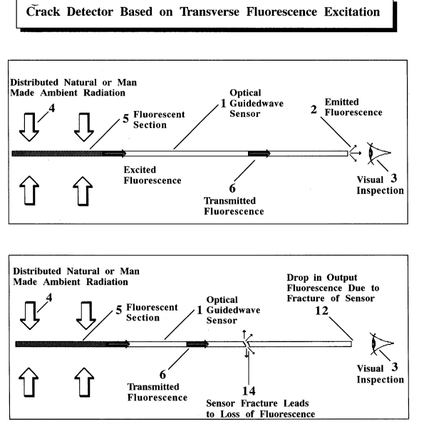
FIG. 4 is a schematic diagram of a plt;fel.~d embodiment of the invention illustrating
transverse excitation through the generation of fluorescence within an optical fiber by ambient
radiation and crack detection through loss of the transmitted radiation.
FIG. 5 is a schematic diagram of an alternative preferred embodiment of the invention
illustrating detection of corrosion at some location along the optical fiber by the disappearance of its
shielding metal coating allowing the generation of fluorescence through transverse excitation at this
location by ambient radiation.
21~831S
Detailed Description of the Preferred Embodiments
The invention involves the following novel features:
1. Distributed transverse excitation allows use of low level ambient radiation and avoids
connection of a man made radiation source to one end of the sensor.
2. The combination of distributed transverse excitation with visual inspection makes possible a
stand alone, self-contained sensor having no connections.
3. Transverse excitation of the sensor allows distributed sensing through the mechanism of
modifying the exposure to the ambient pumping radiation by a change in the measurand of
interest, the state of the sensor, or the local condition to be detected.
Although the invention will now be specifically described with respect to optical fiber sensors,
it is to be understood that the invention is not limited to such devices and can apply to other
guidedwave structures, such as thin films.
Ambient radiation at around 400 nm can excite green {490 nm } fluorescence in plastic fibers.
A good example are the polymethylmethacrylate {PMMA}clad-polystrene core fibers manufactured
by Bicron Corporation, Ohio, US. Other wavelength ranges are also possible. Distributed
transverse excitation over about a 3 cm length of these fibers by ambient radiation, even in the
evening of a cloudy day, produces sufficient intensity for them to be used as a sensor with either
visual or photodetector monitoring. FIG. 1 presents a schematic illustration of one preferred
embodiment of our invention in which a length of optical fiber 1 transmits the optical signal to the
output end 2 where visual inspection 3 is employed. For the case illustrated in FIG. 1 the
distributed ambient radiation 4 transversely excites the fluorescent section 5 {which may, or may
not, be made of the same material as the rest of the optical fiber}and generates a fluorescent signal
6 that is transmitted to the output end 2. In FIG. 2 a Bragg grating 7 is shown to redirect the
distributed ambient radiation 8 along the length of the optical fiber 1 towards the output end 2,
while in FIG. 3 a scattering section 10 is employed to redirect the distributed ambient radiation 11.
As this optical signal {6, 8 or 11 } is guided through the sensing section of the optical fiber it
iS modified in some manner by the state of the optical fiber, or the measurand of interest. For
example, in FIG. 4, we show that if the fiber is fractured 14 by a crack to be detected in some host
material to which the optical fiber is surface adhered or embedded, there is a sudden loss of
fluorescence 14 and a concomitant drop in the emitted fluorescence 12. Visual inspection, or
monitoring by a photodetector would then provide information on the state of the fiber and its host
material. This could be used as the basis of a structural integrity sensor that could be designed to
detect cracks in metal structures, debonding of joints or repair patches, or del~min~tions in
advanced composite materials. Lymer et al., 1990 [US patent # 4,936,649] demonstrated a
method of tailoring optical fibers to match the damage observed in Kevlar/epoxy. Alternatively,
the optical fiber might be bent so as to introduce loss through radiation modes and thereby reduce
the radiation transmitted to the detection end. In this way the optical fiber can be used to measure
deflection of a structure, or a change in pressure applied to the sensor.
In another preferred embodiment a section of multimode fluorescent optical fiber 5 is shielded
by a specially designed coating from exposure to ambient natural, or a man made radiation source.
When this coating is exposed to: a specific chemical, or corrosion, or a threshold temperature, its
shielding properties are modified so that the fiber is excited to fluoresce and ilhlminate the
remAining length of the optical fiber. The degree of exposure to the environmental change is
gauged from the optical power emitted from the output end of the sensor. In FIG. 5 we illustrate
the case for the detection of corrosion of a metal structure. In this example the fluorescent section
5 is shielded from the ambient radiation by a metal coating 15 that is designed to be destroyed at
the same rate as the host material. Thus initially no fluorescence is observed from the output end
of the sensor 16 but as corrosion proceeds to destroy the metal coating 17 fluorescence is seen at
the output end. Some degree of quantification of the extent of corrosion may be possible from the
extent of the observed fluorescence. It is clear that the same principle can be applied to the
2128315
detection of specific chemicals that might dissolve a coating, or erosion of a surface, or the
exceedance of a threshold temperature that melts, evaporates or sublimes the shielding coating at
the applupliate temperature.
The opposite affect, that is the build up of some film or layer, from dirt to a semiconductor
material in an MBE machine, could be assessed from the extinction of the output signal of an
optical fiber that is suitably positioned. Since absoutely no form of electronics is required in the
visual inspection mode this type of sensor might also find application in very high electric and
magnetic field environments. It is also possible to use the invention to monitor exposure to a
variety of environmental conditions such as the level of X-rays or other forms of radition from the
degradation of the output signal. Degradation of the sensor may also be used to monitor the
cummulative affects of periods of exposure to an elevated temperature.
One of the advantages of this invention is the elimination of the need to connect a light source
to one end of the optical fiber. This greatly simplifies the design, installation and cost of the
sensor. When used with visual inspection the sensor is completely self-contained and requires no
connection making it extremely low cost, simple to install and very easy to use. Another advantage
of this invention is that there is very little to go wrong, particularly, when using natural ambient
radiation combined with visual inspection. The light source is obvious and so the observer
provides the detector. These attributes open broad areas of application where conventional fiber
optic sensors would not be practical or desirable. Degradation of the optical fiber might be one
source of error but this could be checked with the manufacturer.
In many applications it may be desirable to use a reference system. This is particularly the case
where the intensity of the output power is intended to convey some sensing information rather than
just the presence or absence of an optical output, and variations in the ambient radiation is possible.
A reference system would comprise a similar length of optical fiber as the sensing optical fiber,
especially the excitation section, and be exposed to the same ambient radiation. However, it would
be designed to not respond to the condition, or measurand, of interest.
It will be apparent that many other changes may be made to the illustrated embodiment, while
falling within the scope of the invention and it is intended that all such changes be covered by the
claims appended hereto.