Note: Descriptions are shown in the official language in which they were submitted.
"l0 93/15424 PCT/GB93/00121
2128534
1
ALIGNMENT OF' INTEGRATED OPTICAL COMPONENTS
This invention relates to the alignment of components such
as integrated optical components.
Difficulties are commonly experienced in mounting together
integrated optical components (such as a semiconductor
laser with optical fibres or planar waveguides, detectors,
fibre amplifiers and the like), with sufficient accuracy.
One of the moat demanding situations is the provision of
accurate alignment between a laser and waveguides. As an
example of this requirement, the case of a semiconductor
laser couplin<3 to an AsG waveguide has been considered.
For maximum power transfer, the laser and guide should
exactly butt together. The coupling efficiency is limited
by t he mi smat <:h i n t he mode s i zes of t he two component s .
For the structures of current interest, this results in an
efficiency of 45~ or' a loss of 3.5dB.
In practice, it is not possible to achieve exact butt
coupling and it is therefore necessary to determine the
opt imum separat i on between t he 1 aser and t he gui de where
axial alignment sensitivity is at its lowest. For
signalling type applications, a coupling efficiency between
the laser and waveguide of 10~ or a loss of lOdB is seen as
the minimum acceptable value. Taking this figure as a
SUBS l I l UTE SHEET
WO 93/15424 PCT/GB93/00121
21~853~
2
target specification, the maximum horizontal and vertical
misalignment allowable has been calculated as a function of
separation between the laser and the waveguide. For the
current case, it was found that a separation of Gum gave
the lowest sensitivity to axial misalignment (l.7um or
l.9um in the vertical or horizontal directions before loss
in excess of the target value was obtained).
These calculations do not take into account any angular
deviation between the laser and the waveguide and so should
be viewed as a "best case" estimate. As a result, the
alignment tolerance sought in a motherboard process was
taken as less than 1um in both the horizontal and vertical
directions. If higher coupling efficiencies than 10~ are
required, (eg in the case of laser pumping for optical
amplifiers), it would be necessary to match the mode sizes
of the two components by use of, for example, a Tensed
laser assembly.
It has been known to join two integrated circuit or chips
by a so called "flip-chip" solder bonding technique. The
faces of the two integrated circuits which are to be joined
each contain a corresponding pattern of metal pads, and one
of the integrated circuits is provided with a solder bump
on each metal pad, the two integrated circuits are
approximately aligned, the solder is melted, and the
solder, by surface tension, moves the two integrated
SUSSiI~UiE SHEET
21 2853 4
3
circuits into alignment so that the corresponding metal pads on each
integrated circuits are exactly aligned. The alignment is determined by the
metal pads themselves. Whilst this provides a fairly accurate way of
aligning two components, in particular in a case with flip-chips where the
two integrated circuits are 1.o be interconnected electrically, as determined
above, greater accuracy of alignment is required in aligning integrated
optical components.
The present invention provides, according to one aspect, a method of
connecting first and second components together with functional parts
thereof in a predetc:rminecl alignment;
the first component having a first functional part and a pad on the
surface of said first component,
the second c~omponE:nt having a second functional part and a pad on
the surface of said secondl component,
one of said pads being provided with a meltable solid, the meltable
solid being of a material which preferentially adheres to the pads;
said first component including a first alignment means in a
predetermined position with respect to said first functional part;
said second component including a second alignment means in a
2o predetermined position with respect to said functional part;
said first anc~ second alignment means being formed so as to be
mutually engageahle so that first alignment means may abut second
alignment means,
the method comprising the steps of; generally aligning the two
components and melting the meltable solid so that it interconnects
corresponding pads on the two components, wherein the disposition of the
first and second ~ilignment means and pads is such that the surface
tension of the molten solid in contact with adjacent pads on the two
components urges the two components into a relative position so that the
A
21 2853 4
4
first and second alignment means abut each other and thereby accurately
align so that the first and second functional parts are in a predetermined
alignment.
Preferably, said pads are disposed so that when said two components are
aligned, the surface tension of said molten solid continues to provide a
component of force whiclh urges the alignment means into contact with
each other.
Preferably, in respect of one or both components, the functional parts are
1o also defined by the same etching step as the alignment means.
There are very considerable advantages in the method of the invention.
Thus the alignment means will be reproducibly accurately aligned with the
functional part of the component as they are made by the same process.
Thus for example, where one of the components is a semiconductor
A
°
'~VO 93/15424 21 ~ 8 ~ 3 4 PCT/GB93/00121
laser, the radiation output of the laser (which is the
functional part), is defined in an etching process step
which may al~;o be used to provide the alignment means.
Similarly, if the component is a silicon motherboard, the
5 input of a waveguide (which for this purpose is the
functional part ) is defined in our etching step which is
also used to define the alignment means.
The method is compatible with conventional silicon
:LO processing, that is wet and dry etching and
photol ithography requi rements.
In accordance with conventional techniques, the etching may
be carri ed out aft ear a resi st 1 ayer has been 1 ai d on t he
:l5 surface by photol i t hography.
In a preferred arrangement, each component may include two
alignment means, to operate in orthogonal directions.
:20 The alignment means may comprise a protrusion, an edge, or '
a slot. In a preferred arrangement, one of the components
may comprise a substrate of crystalline material which
contains intersecting planes which can be delineated by
etching, the etching of the alignment means forming the
:25 alignment means.
The present vnvention also provides in combination, two
SUuSTi T U T E SHEET
2128534
components mounted together, each component comprising a
functional part and an alignment means in a predetermined
position with respect of said functional part. each
component including a pad in a predetermined position on
its surface, said two components being interconnected by a
molten. solid extending between adjacent pads on the two
components, said combination being formed in accordance
with a method as clam--~d in any of claims 1 to 7.
,0 The invention will now be described by way of example only
and with reference to the accompanying drawings in which:-
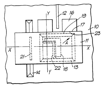
Figure 1 is a diagrammatic plan view of part of a
- _ motherboard with semiconductor laser mounted thereon in
accordance ~Hith a method of the invention,
Figure 2 is a section of Figure 1 on line Y-Y, and,
Figure 3 is a section of Figure 1 on line X-X.
Referring to Figure 1 there is shown a silicon motherboard
- 10 on top o~~ which is to be mounted a semiconductc;- layer
11. In the process of the invention, various comp~nents
are formed on the silicon of the motherboard 10, for
example, a waveguide 12. The optical waveguide 12 is
defined on a silicon motherboard by a lithographically
patterned As~~ core surrounded by an undoped silicon dioxide
cladding. -'his combination of glasses can be processed
conveniently at low temperatures, and owing to their large
index difference" allow the fabrication of low loss, small
suss .. ; a ;v shE~T
WO 93/15424 ~ ~ ~ PCT/GB93/00121
7
radius bends whiclh permit a high component density on the
motherboard.
The process sequence includes initially forming the recess
13 by a micromach,ining or wet etch process. The waveguide
12 is produced by a wet etch process using a KOH chemically
etched recess (typically 7pm deep) which is partially
filled with a PECVD undoped silicon oxide for the low
cladding or buffer- layer. The waveguide core is formed by
a 2pm thick AsG layer which is dry (plasma) etched and
reflowed in an oxidising atmosphere at temperatures between
950 and 1iJ00~. This plasma dry etching process also
defines a mask for subsequently forming the slot 14 to be
referred to later. The end of the waveguide which needs to
be accurate is formed by plasma etching.
A 4 to Gum undoped oxide is deposited to surround the
waveguide core. Potential difficulties arising from
cavities between i:he core and cladding may be minimised by
using planarising techniques.
Micromachining or wet etching is then used through the
defined mask to form the V groove 14 which is thereby
accurately aligned with the waveguide 12.
The recess 13 and V groove 14 are both formed by
micromachining by an anisotropic etching process using an
SuE~-~~; . :: ;-~ SHEET
WO 93/15424 PCT/GB93/00121
~1~g53 4
8
et chant such as KOH or et by 1 ene d i ami ne pyrocat echo 1 and
water (EDP). With such et chants, some crystal planes in
silicon etch much more slowly than others. Consequently
when a masking window is realigned correctly along the
i ntersect i ons of two such 'p1 anes wi t h t he surface of t he
silicon, etching terminates at these planes and a V shaped
groove results. Since these planes are related directly to
the crystal lographic structure of the si 1 icon, the angle
and direction of the recess 13 or V groove 14 are very
tightly controlled. The width of the V groove can
therefore be controlled very accurately, typically to a
tolerance of 0.25 to 0.5 arm. As the mask window for the V
groove 14 is etched in the same step as the waveguide 12 is
etched, the position of the V groove 14, and in particular
the sides of the V groove 14 can be accurately
predetermined with respect to the position of the waveguide
12, by utilising photolithography.
It will be seen from Figure 1 that the V groove 14 is
straight (as would be expected as it is along a crystal
plane) and of a suitable depth as will be determined.
There is also provided on the top surface of the
motherboard 10 a pair of polysilicon stops 16 which are
formed by providing a layer of polysilicon and etching away
(before the wet etching of the "V" groove 14 and just
before the plasma etch of the end surface of the waveguide)
SUESii~Ui~ SHEET
~WO 93/15424 PCT/GB93/00121
2128534
9
the remainder of the layer to provide the polysilicon
stops. Once again, because the polysilicon stops are
provided by means of an etching process through a mask, the
edges 17 01= the polysilicon stop 16 will be accurately
aligned with, for example, the input of the waveguide 12.
A metal pad 18 of "L" shape is laid down in the recess 13,
in a manner well known in semiconductor technology, one leg
of the pad extending parallel to the V groove and the other
leg extending paral lel to the edges 17 of the polysi l icon
stops 1 6.
Referring now to the semiconductor laser 11, there is
provided an active region (viz, output) at which the laser
radiation is outputted adjacent the waveguide 12. The
under surface of 1_he semiconductor laser, includes a ridge
21 downwardly depending from its lower surface. The ridge
21 is produced by an etching process, the etching being
carried out as described above. As the active region 19 of
the laser is also defined by an etching process, the
alignment of the active region 19 and the ridge 21 is
predetermined by t:he masks used in the etching process and
can therefore be accurately determined.
There is al:;o laid down on the under surface of the laser
11 a metal pad c2 which is of similar shape and extent to
the metal pad 18,, that is, "L" shaped with a first leg
SUES ivv s :. SHEET
WO 93/15424 PCT/GB93/00121
~1~g53 ~
parallel to the ridge 21 and a second leg parallel to an
edge 23 of the laser, except that the width of the legs of
the pad 22 are smaller, typically one third, of the width
of the legs of the pad 18.~~.
5
The position, and shape of the metal pads 18 and 22 is
defined in the manufacture of the relevant component by
photolithography through a suitable mask. Furthermore, the
metal pads are made of, or coated with, a metal which is
10 wetted by molten solder.
When the motherboard and laser are correctly aligned, as is
exaggerated in the view of Figure 1, the metal pad 22 is,
in the view of Figure 1, slightly below and to the left of
the metal pad 18._
Before assembly of the motherboard 10 and the semiconductor
laser 11, the metal pad 22 is provided with solder 26 in
the form of a solder bump.
To assemble the semiconductor laser 11 to the motherboard
10, the laser 11 is laid onto the motherboard in
approximate alignment with its final position. In
practice, the laser 11 will naturally rest below and to the
left of the final position in Figure 1, because it cannot
rest on top of the polysilicon stops 16 and the ridge 21
will naturally rest somewhere towards the middle of the V
SUCSTI T UTE SHEET
WO 93/15424 212 8 5 3 4 P~/GB93/00121
11
groove 14. The solder is then melted, and by means of
surface tension effects (see solder 26 in Figures 2 and 3),
wi 11 i nter<:onnect the two metal pads 18 and 22, and draw
the laser 11 in the direction of the arrow A in the Figures
so that the ridge 21 engages against the right side of the
V groave 1.4 as shown i n Fi gure 3 and t he edge 23 of t he
laser abuts the edges 17 of the polysilicon stop 16. In
this way the semiconductor laser 11 is accurately aligned
wi t h t he m~~t he rboa rd 1 0 so t hat t he act i ve reg i on 1 9~ i s
accurately alignead with the waveguide 12.
In the final aligned position of the laser 11 and
motherboard 10, it may be arranged that the two metal pads
18,22 exactly align with one another. Alternatively, it
can be arr~~nged i:hat the metal pad 22 may, when viewed in
Figure 1, be arranged to be below and to the left of the
metal pad 18 (exaggerated in the Figures) whereby even when
the laser 11 and motherboard 10 are correctly aligned,
there will be some residual slight force caused by the
surface tension .effects of the molten solder, urging the
laser 11 in an direction of arrow A.
In some circumstances, it may be that the laser 11 may have
a large surface overlapping and laying on the motherboard
10 and there may be frictional forces to be overcome if the
laser and motherboard are to be moved relative to one
another. In this case, one solution is for the quantity of
SUESTI T UTE SHEET
WO 93/15424 PCT/GB93/00121
12
solder in each solder bump to be greater than otherwise so
that when the solder melts, there is sufficient solder to
cause t he l ase r 1 1 t o be ~l i ft ed above t he mot he rboard 10 t o
thereby eliminate friction. The amount by which the laser
is lifted above the motherboard is preferably very small,
typically 1um and therefore the amount of solder in each
solder bump should be carefully calculated to provide that
exact clearance between the laser and motherboard. In this
way, by eliminating friction particularly to zero, the
surface tension effect is sufficient to move the laser with
respect to the motherboard exactly into alignment as above
described.
We have therefore provided a method of connecting external
components such as lasers, detectors, and/or other optical
integrated circuits to a motherboard. The process is
compatible with conventional silicon processing and
photolithography. The use of surface tension in molten
solder to move the semiconductor laser 11 into correct
alignment with the motherboard 10 enables one to use a
controlled force to move the laser. Excessive force could
cause damage to the alignment means, in particular the
ridge 21 which might easily be damaged or broken.
In an alternative arrangement, the pad 18 may also be made
thinner than the pad 22 in which case their orientations
would need to be rotated by 180° in respect of the view in
SJ~~Ti ; JT~ SHEET
1N0 93/15424 ~ ~ ~ ~ ~ PCT/GB93/00121
13
Figure 1.
The invention is not restricted to the details of the
foregoing example.
The two pads 18 and 22 are shown "L" shaped in the present
arranged. However the two pads could be other shapes, for
example rectangular but they should have the relative
orientation shown in Figure 1, that is the pad 18 is (in
the plane of the drawing) further up and to the right with
respect to the padl 22.
The invention is not restricted to the details of the
foregoing example.
SUBSTI T UTE SHEET