Note: Descriptions are shown in the official language in which they were submitted.
~3/14~20 2 1 2 ~ PCT/US93/00497
INTEGRATION OF TRANSISTORS WITH
VERTICAL CAVITY SURFACE EMITTING LASERS
CROSS REFERENCE TO RELATED APPLICATIONS
This application is related to our co-pending
application serial No. 07/790,964, filed November 7, :~
1991, for "Visible Light Surface Emitting
Semiconductor Laser" and to our application serial no.
_ , filed concurrently herewith, for
10 IlVertical-Cavity Surface Emitting Laser Optical ~-~
Interconnect Technology," which are incorporated
herein by reference.
FIELD OF THE INVENTION
This relates to the integration of semiconductor ~
lasers with electronic devices. In particular, it `-
relates to vertically arranged heterostructure lasers
and their integration with devices such as
transistors.
BACKGROUND OF THE INVENTION
Conventional edge-emitting laser diodes are well
known. In these diodes, laser radiation is emitted in
a plane that is a continuation of the plane of the p-n
junction that forms the diode. Different types of
these diodes are widely used to provide laser
radiation in the infrared and visible regions. While
these diodes have enjoyed considerable commercial
success, they are relatively large and, as a result,
are difficult to integrate with other devices.
Recently, a new class of semiconductor lasers
known as a vertical cavity surface emitting laser has
been developed. Unlike the edge-emitting laser, these
vertical cavity lasers emit laser radiation in the `
direction perpendicular to the plane of the p-n
WO93/14~20 PCT/US93/0049
~,~'8`~ 2 -
junction formed in the laser diode. Considerable ~
information concerning the structure and formation of -
such laser diodes is set forth, for example, in U.S.
Patent 4,949,350; in J. Jewell et al., "Microlasers,
" Scientific American, Vol. 265, No. 5, pp. 86-94
(November 1991); in J. Jewell et al., "Vertical-Cavity
Surface-Emitting Lasers: Design, Growth, Fabrication,
Characterizationl " IEEE Journal of Ouantum ~-~
Electronics, Vol. 27, No. 6, pp. 1332-1346 (June
1931); in G.R. Olbright et al., "Cascadable Laser
Logic Devices: Discrete Integration of Photo-
transistors with Surface-Emitting Laser Diodes,"
Electronics Letters, Vol. 27, No. 3, pp. 216-217
(January 31, 1991); in J. Jewell et al., "Low-
threshold Electrically-Pumped Vertical-Cavity Surface
Emitting Lasers," Electronics Lett., Vol. 25, p. 1123 ~
(1989); and in J. Jewell et al., "Vertical Cavity -
Lasers for Optical Interconnects," SPIE Vol. 1389
International Conference on Advances in
Interconnection and Packaaina, pp. 401-407 (1990), all
of which are incorporated herein by reference.
As`set forth in certain of the above-referenced
publications, vertical cavity lasers have numerous
advantages over edge-emitting lasers, some of the most
important of which are that they can be fabricated in
extremely small sizes (e.g., on the order of one
micrometer in diameter) and can be integrated with
other devices such as transistors.
SUMMARY OF THE INVENTION
The present invention is directed to such
integration of vertical-cavity lasers. We have
invented vertical-cavity lasers that are integrally
formed with electronic switches such as three-terminal
transistors.
~ ~3/14520 212~ i3 :~ PCTtUS93/00497
- 3 -
In a preferred embodiment of the invention, a
vertical-cavity surface-emitting laser ~VCSEL)
comprises a laser cavity sandwiched between two
distributed Bragg reflectors. The laser cavity
comprises a pair of spacer layers surrounding one or
more active, optically emitting quantum-well layers
which serve as the active optically emitting material
of the device. The thickness of the laser cavity is
m~/2ne~r, where m is an integer, ~ is the wavelength of
lo the laser radiation and nef, is the effective index of ~-
refraction of the cavity. Electrical pumping of the --
laser is achieved by heavily doping the bottom mirror
and substrate to one conducti~ity-type and heavily
doping regions of the upper mirror with the opposite
conductivity type to form a diode structure and
applying a suitable voltage to the diode structure.
The switch may take any number of forms and can
be located in various positions relative to the VCSEL.
The switch may be an electronic switch such as a
bipolar transistor or a field effect transistor. In
the case of the bipolar transistor, the transistor can
be located underneath, on top of, or alongside the
VCSEL, just like the photo-transistor. In the case of
a field effect transistor, the transistor is located -~
alongside the VCSEL.
The switch may also be an optical switch such as
a photo-transistor located alongside the VCSEL. ;
Combinations of optically controlled and
electrically controlled switches may also be
implemented in accordance with the invention.
The integrated switching of the present invention
provides a convenient means for controlling the output
of laser radiation from the VCSEL with either optical
or electrical signals. Boolean logic functions can
readily be implemented by these switches; and signal
WO93/14520 PCT/US93~0049
~ 3l,J - 4 ~
amplification and ~onversion from electrical to
optical or optical to electrical is easily achieved. -~
BRIEF DESCRIPTION OF THE DRAWING
These and other objects, features and advantages
of the invention will be more readily apparent from
the following detailed description of the invention in -
which: `
Fig. 1 is a schematic illustration of a prior art
10 vertical cavity surface emitting laser, ~-
Figs. 2A, 2B and 2C are schematic illustrations
of an optoelectronic integrated circuit which combines
a vertical cavity surface emitting laser with an
heterojunction bipolar transistor;
Fig. 3 is a more detailed illustration of the `
integrated circuit of Fig. 2A; ;~
Fig. 4 is a circuit schematic for the integrated
circuit of Fig. 3;
Fig. 5 is a top view of the integrated circuit of
Fig. 3;
Fig. 6 is a more detailed illustration of the
integrated circuit of Fig. 2B;
Fig. 7 is a top view of the integrated circuit of
Fig. 6;
Fig. 8 is a more detailed illustration of the
integrated circuit of Fig. 2C;
Fig. 9 is a top view of the integrated circuit of
Fig. 8;
Fig. 10 is a schematic illustration of an
30 optoelectronic integrated circuit which combines a -
vertical cavity surface emitting laser and a field
effect transistor;
Fig. 11 is a more detailed illustration of the
integrated circuit of Fig. 10;
93/14520 212 8 ~ J PCT/VS93/00497
- 5 - ;
Fig. 12 is a top view of the illustrative
embodiment of the integrated circuit of Fig. 11;
Fig. 13 is a schematic illustration of an
optoelectronic integrated circuit which combines a
5 vertical cavity surface emitting laser with a photo- -~
transistor; and
Fig. 14 is a more detailed illustration of the
integrated circuit of Fig. 13. !".
DETAILED DESCRIPTION
As shown in Fig. 1, a prior art vertical-cavity -~
surface emitting laser (VCSEL) comprises a first n+
mirror layer 10, a first spacer layer 20, a quantum
well layer 30, a second spacer layer 40 and a second
p+ mirror layer 50. Following techniques known in the
art and described, for example, in the
above-referenced U.S. Patent 4,949,350, layers lo, 20,
30, and 40 and a portion of layer 50 axe epitaxially
formed on a substrate 60. The remaining portion of ~;
layer 50 is formed by dielectric deposition. As a
result, layers 10, 20, 30, 40, and 50 have the same
diameter as substrate 60.
Advantageously, a confinement region 33 is
defined in the periphery of quantum well layer 30 by
proton implantation so as to confine current flow in
the laser to a narrow region around the central
vertical axis of the laser. After the epitaxial
formation of the layers, ~uan~um well layer 30, spacer
layer 40, and mirror layer 50 are defined by optical
lithography and etching to form a plurality of columns
70. Electrical contacts to second mirror layer 50 and
substrate 60 are provided at 56 and 66. Each column
70 is a separate laser and can be made to lase by
applying a suitable voltage between contact 66 and
WO93~14520 PCT/US93/0049-
~ 6 -
contact 56 of that column to drive sufficient current
through the column. -
Illustratively, substrate 60 is a wafer of N+
doped GaAs having a diameter of 3 or 4 inches (7.5 or -~~
lO cm.) during epitaxial processing; and, each column
is about 20 micrometers in diameter and about 2.5
micrometers high above the surface of spacer 20. The ~
wafer is ordinarily diced into several units for use. ~-
Each of layers lO, 20, 30, 40, and 50 comprises a ~-
plurality of layers. For example, for the case of a
red-light emitting vertical-cavity laser disclosed in ~-
our co-pending application serial no. 07/790,964,
mirror layer lO comprises alternating layers of n+
doped AlAs and AlGaAs, each layer being a ;
lS quarter-wavelength thic~ where the wavelength is the
wavelength in the layer of the radiation being emitted
by the laser. As will be recognized by those skilled
in the art, the construction of mirror layer lO is
that of a distributed Bragg reflector in which the
AlAs is the layer having the lower index of refraction
and AlGaAs is the layer having the higher index of
refractiQn. Mirror lO is designed so that it is
completely reflective and has no transmission.
Spacer layer 20 comprises a plurality of layers
of AlGaInP with progressively increasing amounts of Ga
toward the quantum well layer. As is known in the
art, these layers are lattice matched to the GaAs.
Spacer layer 40 is similar in construction with
progressively decreasing amounts of Ga toward mirror
layer 50. Quantum well layer 30 comprises three
approximately 50 Angstrom thick layers of GaInP
separated by two approximately 90 Angstrom thick
barrier layers of AlGaInP. Spacer layer 20, quantum
well layer 30, and spacer layer 40 constitute the
laser cavity. The length of the laser cavity (which
~3/14520 7 2~ 2$ ~ PCT/US93/00497
is the thickness of layers 20, 30, and 40) is m ~/2n
where ~ is ~he free space wavelength of laser
radiation emitted, m is an integer and n~, is the
effective refractive index of the cavity.
Second mirror layer 50 comprises a plurality of ~-
alternatinq layers of p+ doped AlAs and AlGaAs. ~;
Again, each of these layers is a quarter-wavelength -
thick and these layers constitute a distributed Bragg
reflector. The reflector, howeverj is partially
transmissive to provide for the emission of laser
radiation from the uppermost layer.
Numerous other VCSEL structures havP been
demonstrated and reported in the literature. See, for
example, the references cited in the Background of the
InYen~ion and the disclosure in our concurrently filed
application serial no. In general, any of
these structures can be used in the practice of the ~-
invention.
In accordance with the invention, optoelectronic ~-
integrated circuit devices are formed by combining
VCSELs with three-terminal transistors. In addition,
integrated circuits are also disclosed in which VCSELS
are combined with heterojunction photo-transistors in
novel combinations.
As shown in Fiqs. 2A, 2B and 2C, a VCSEL may be
combined with a heterojunction bipolar transistor
(HBT) in any one of three ways. In Fig. 2A, an
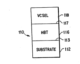
optoelectronic inteqrated circuit 110 is formed on a
substrate 112 by forming an HBT 116 on an upper
surface 113 of the substrate and by forming a VCSEL
118 on an ~pper surface 117 of the transistor. In
Fig. 2B, an optoelectronic inteqrated circuit 120 is
formed on a substrate 122 by forming a VCSEL 128 on an
upper surface 123 of the substrate and by forming an
HBT 126 on an upper surface 127 of the VCSEL. In Fig.
~ c,~3`) - 8 - PCT/US93/0049- `
2C, an optoelectronic integrated circuit 130 is formed
on a substrate 132 by forming a VCSEL 138 on a first
portion 133 of an upper surface 135 of substrate 132
and by forming an HBT 136 above a second portion 134
of the upper surface 134 of substrate 132. Further
details of these combinations are set forth in the
figures immediately following.
Fig. 3 depicts in greater detail integrated
circuit 110 in which a VCSEL 118 is formed on an HBT
lo 116 on a substrate 112. As shown in Fig. 3, VCSEL 118
comprises a partially transmissive mirror 141, a p- ~
type spacer 142, a quantum well region 143, an n-type ~"
spacer 144 and an n-type mirror 145. Advantageously,
the active portion of the quantum well region is
narrowed by a peripheral confinement region (not
shown) similar to confinement region 33 of Fig. 1. As
noted in the discussion of Fig. 1, each of the
mirrors, spacers and quantum wells of the VCSEL is
made of several layers. Heterojunction bipolar
transistor 116 is an n-p-n transistor comprising an n-
type collector layex 146, a p-type base layer 147, and
an n-type emitter layer 148. Circuit 110 further
comprises an annular contact 149 to the upper surface
of spacer 142, an annular contact 152 to base layer
147 and an n-type ohmic contact 155 to substrate 112.
Circuit 110 is formed by depositing the layers of
elements 141-148, one on top of the other beginning -~
with layer 148, on top of substrate 112. The layers
of elements 142-148 are formed on substrate 112 by
epitaxial growth using techniques well known to those
sXilled in the art and described, for example, in U.S.
Patent 4,949,350. The layers of mirror 141 may also
be epitaxially grown. However, one advantage of the
structure of Fig. 3 is that mirror 141 is not part of
the electric circuit that biases the VCSEL. As a
~ ~3/14520 ~ 12 ~ ~; r~ ) PCT/US93/00497
result, unlike mirror 145 which must be made of
semiconductive materials since it is part of the
biasing circuit, mirror 141 can be made of a much
wider variety of materials and, in particular, can be
made of dielectric materials.
Illustratively, substrate 112 is made of n-type
GaAs and photo-transistor 116 is a GaAs photo-
transistor comprising an emitter layer of n-type ~
AlGaAs approximately 0.2 micrometers thick, a base ~-
layer of p-type GaAs approximately 0.25 micrometers
thick, and a collector layer of n-type InGaAs/GaAs
approximately 0.5 micrometers thick. Illustratively,
VCSEL 118 is similar to that described in conjunction
with Fig. 1 and includes mirrors comprising a
plurality of alternating layers of AlAs and AlGaAs,
spacers of layers of AlGAAs, and a quantum well layer
made of layers of InGaAs separated by barrier layers
of GaAs.
Following the deposition of the layers,
individual integrated circuits 110 are defined by
photolithographic and etchinq techniques. First, the
upper mi~rors of the circuits are defined by removing
unwanted portions of these mirrors down to the upper
surface of spacer 142. Next, the material of contact
149 is deposited; and the contact is defined by
removing unwanted portions of the deposited material.
The individual VCSELs are then defined by removing
unwanted portions of spacers 142, 144, quantum well
143, mirror 145 and collector layer 146. The material
of contact 152 is then deposited on the exposed
surface of base layer 147. Finally, contact 152 is
defined by removing unwanted portions of the deposited
material.
When a suitable voltage VO is applied between
contact layer 149 and substrate 112 of circuit 110,
WOg3~14520 ~ PCT/US93~0049
~ 3" - 10 -
the circuit will operate as an electrically switched
laser. A schema~ic diagram of the circuit is shown in
Fig. 4. As shown, the circuit comprises HPT 116,
VCSEL 118, and resistor Rn which is the electrical
5 resistance of mirror 145. --
When sufficient electrical current te.g., tens of
micro-Amps)is supplied to base layer 147 of HBT 116,
the transistor becomes conducting, with the result
that there is substantial current flow ~several milli-
Amps) through VCSEL 118. This causes VCSEL 118 tolase, emitting laser radiation (about one milli-Watt)
through partially transmissive mirror 141.
A top view of an array of the integrated circuits
110 of Fig. 3 is shown in Fig. 5. Advantageously,
contact 152 extends around the periphery of the base
of VCSEL 118. Contact 149 is annular in shape and
surrounds upper mirror 141 of the VCSEL. Various
arrangements may be made to establish electrical
connection to contacts 149 and 152. In the
illustrative embodiment of Fig. 5, contact 149 is
connected to a common bus 150 to which a biasing
voltage ~O is applied to bias all the VCSELs in the
array. Illustratively, each contact 152 is connected
by an individual lead 153 to a separate bonding pad
(not shown) so that individual control signals may be
applied to the base of each VCSEL.
Fig. 6 depicts in greater detail integrated
circuit 120 in which an HBT 126 is formed on a VCSEL
128 on a p-type substrate 122. As shown in Fig. 6,
HBT 126 is a n-p-n transistor comprising an n-type
collector layer 166, a p-type base layer 167 and an n-
type emitter layer 168. VCSEL 128 comprises a
partiality transmissive p-type mirror 161, a p-type
spacer 162, a quantum well region 163, an n-type
spacer 164 and an n-type mirror 165. Again, each of
93/14520 PCT/US93/00497
the mirrors, spacers and quantum well of VCSEL 128 is
made of several layers; and the active por~ion of the
quantum well region is advantageously circumscribed by
a confinement region 163'. Circuit 120 further
comprises contact 169 on the upper surface of emitter
layer 168, an annular contact 172 on the upper surface
of base layer 167 and a p-type ohmic contact 175 to
substrate 122.
As will be apparent from a comparison of Figs. 3
~0 and 6, circuit 120 is similar to circuit 110 except
that the VCSEL and HBT have been inverted and the
electrical contacts have been changed. Fabrication of
circuit 120 is similar to that of circui~ 110 with
appropriate changes in the order of deposition of the
15 layers to achieve the difference in structure. ~`
Operation of circuit 120 is th~ same as the operation
of circuit 110 but the bias voltage is -VO instead of
VO- ~.
Circuit 120 has the advantage that it can be -
fabricated more easily than circuit 110 because it is
not necessary to make a deep etch to access the base
layer to form the contact thereto. Rather, it is only
necessaxy to remove unwanted portions of emitter layer
168. Circuit 120 can be isolated from adjacent
circuits on the same substrate by etching as done for
the devices of Figs. 1 and 3 or by conventional ion
implantation techniques. ~-
A top view of a two dimensional array of
integrated circuits 120 is shown in Fig. 7. In this
illustrative embodiment, each contact 169 is connected
to a common row bus 170 to which a biasing voltage - V~,
is applied to bias all the VCSELs in that row of the
array. Each contact 172 is connected by an individual
lead to a common column bus 173. The row and column
buses are electrically isolated from one another. As
WO93/14520 , - 12 - P~/US93/0049-
'3~ ~
a result of this arrangement, an x-y addressing scheme
is provided which permits one to selectively activate
any one of the VCSELs in the two-dimensional array.
If desired, other control arrangements could also be ~`
used such as the use of individual control leads to
the base contact as shown in Fig. 5.
Fig. 8 depicts in greater detail integrated
circuit 130 in which HBT 136 is formed alongside VCSEL ~-
138. As shown in Fig. 8, VCSEL 138 comprises a
partially transmissive mirror 181, a p-type spacer
182, a quantum well region 183, an n-type spacer ~84
and an n-type mirror 185. Again, the active region of
the quantum well layer is narrowed by a peripheral
confinement region 183'. HBT 136 is an n-p-n
transistor comprising an n-type collector layer 186, a
p-type base layer 187, and an n-type emitter layer
188. Circuit 130 further comprises a contact 191 to
collector layer 186, an annular contact 192 to base
layer 187 and a contact 193 to emitter layer 188. As
shown in Fig. 8, HBT 136 is formed on top of layers
182-185 of VCSEL 138 and alongside mirror 181 so that
it is off-axis relative to the laser output of VCSEL
138. HBT 136 is electrically isolated from the region
of the VCSEL over which it is formed by an insulating
layer 196 and an ion-implanted guard ring 197 and is
electrically connected by contact 193 to the region of
the VCSEL in which lasing takes place. As suggested
by Fig. 8 and as shown in Fig. 9, contact 193
comprises two interconnected annular contacts, one of
which circumscribes the emitter layer and the other of
which circumscribes mirror 181.
Circuit 130 is formed by depositing the layers of
mirror 185, spacer 184, quantum well layer 183 and
spacer 182 on substrate 132 in that order. Next,
insulating layer 196 is formed on top of spacer layer
U ~3/14520 - 13 2 1 2 ~ ~ ? .~ PCT/US93/004s7
182 and emitter layer 188, base layer 187 and
collector layer 186 are formed on top.
Photolitho~raphic techniques and etching are then used
to define the HBTs and to remove unwanted material
down to spacer 182. The layers of mirror 1~1 are then
deposited and the mirror is defined by
photolithographic techniques and etching. Finally,
contacts 191, 192, 193 are deposited and defined.
In the embodiment shown in Fig. 8, mirror 181
includes the insulating layer 196 as well as the
layers of semiconducting material that were deposited
to form emitter 188, base 187 and collector 186. This
is feasible as long as these ~aterials do not absorb
significant amounts of laser radiation from the VCSEL.
~5 This condition is met if the semiconductive materials
have a higher bandgap energy than the laser frequency.
Alternatively, the materials of layers 186, 187, I88
and 196 can be removed from the area where mirror 181
is to be formed and other materials can be used to
form the layers of this mirror.
When a suitable voltage V0 is applied between
contact i91 and substrate 132 of circuit 130, the
circuit will operate as an electrically switched laser
in the same fashion as circuits 110 and 120.
A top view of a two-dimensional array of
integrated circuits 130 is shown in Fig. 9. In this
illustrative embodiment, contact l91 is connected to a
common column bus 198 to which a biasing voltage V0 is
applied to bias the VCSELs in that column of the
array. Illustratively, each contact 192 is connected
to a common row bus 199. Again, the row and column
buses are electrically isolated from one another. As
a result of this arrangement, an x-y addressing scheme
is provided which permits one to selectively activate
any one of the VCSELs in the two-dimensional array.
WO93/14520 ~ 14 - PCT/US93/0049
As shown in Fig. lo, a VCSEL may also be combined
with a field effect transistor (FET). In this
embodiment an optoelectronic integrated circuit 310 is
formed on a substrate 312 by forming a VCSEL 318 on
one portion 315 of an upper surface 313 of substrate C
312 and by forming an FET 316 above a second portion
314 of the upper surface of the substrate. -
Fig. 11 depicts in greater detail an illustrative
embodiment of such a circuit. As shown in Fig. 11,
10 VCSEL 318 comprises a partially transmissive mirror ~;
341, a p-type spacer 342, a quantum well region 343, ~
an n-type spacer 344 and an n-type mirror 345. Each --
of the mirrors, spacers and quantum well of the VCSEL
is made of several layers; and the active quantum well
is narrowed by confinement region 343'. Field effect
transistor (FET) 316 comprises an n-type FET channel
346 and source, gate and drain electrodes 347, 348,
349, respectively, formed on top of an insulating
layer 350. A guard ring 351 isolates source electrode
347 so that current flow must be through the narrow
region surrounded by confinement region 343'.
As sùggested by Fig. 11 and as shown in the top
view of Fig. 12, the FET surrounds substantially all
of mirror 341 of the VCSEL. This arrangement
advantageously permits the use of an annular gate
electrode having a very long dimension transverse to
channel 346. Since the maximum current through an FET
channel is directly proportional to the transverse
dimension of the channel, this annular geometry is
very useful in providing the current (about 10 milli-
Amps) needed to drive a VCSEL.
Illustratively, substrate 312 is made of n-type
GaAs and FET 316 is a GaAs or AlGaAs FET having a
channel that is approximately 600 Angstrom thick under
the gate electrode. Illustratively, VCSEL 318 is
93/14520 ~1 2~3 J P~T/US93/00497
- 15 -
similar to that described in conjunction with Fig. 1
and includes mirrors comprising a plurality of
alternating layers of doped AlAs and AlGaAs, spacers
of AlGaInP, and a quantum well layer made of layers of ~-
GaInP separated by barrier layers of AlGaInP.
Circuit 310 is made in similar fashion to circuit
130 of Fig. 8 above. The layers of mirror 345, spacer ~
344, quantum well layer 343, spacer 342 and mirror 341 ;
are deposited on substrate 312 in that order. To form
lo the FET, insulating layer 350 is formed on top of
spacer layer 342 and the FET channel is formed on top
of the insulating layer. The layers of the mirror are
then deposited and the shape of mirror 341 is then
défined photolithographically and the deposited layers
15 are removed from those areas not part of the mirror. -~
Finally metallization is deposited and the source,
gate and drain electrodes are formed.
When a suitable voltage VO is applied between
drain electrode 349 and substrate 312 of circuit 310,
the circuit will operate as an electrically switched
laser responsive to voltage signals applied to gate
electrode 348. Application of an appropriate voltage
to the gate electrode will allow enough current to
flow through VCSEL 318 to cause it to lase and emit
laser radiation through mixror 341.
A top view of a two-dimensional array of circuits
310 is shown in Fig. 13. Advantageously, each drain -
electrode is connected to a common row bus 352 to
which a biasing voltage VO is applied to bias all the
VCSELs in that row of the array. Illustratively, each
gate electrode is connected to a common column bus
354. Again, each row and column bus is electrically
isolated. As a result, each VCSEL of the array can be
individually addressed for operation.
WO93/14520 ~ ~``J - 16 - PCT/US93/0049'
Figs. 13 and 14 depict in greater detail
integrated circuit 410 in which a heterojunction
phototransistor (HPT) 416 is formed alongside a VCSEL
418 on a substrate 412. As shown in Fig. 14, VCSEL
418 comprises a partially transmissive mirror 421, a
p-type spacer 422, a quantum well region 423, an n-
type spacer~424 and an n-type mirror 425. HPT 416 is
an n-p-n transistor comprising an n-type collector
layer 426, a p-type base layer 427, and an n-type
emitter layer 428. Circuit 410 further comprises a
transparent contact 431 to collector layer 426 and an
annular contact 433 to emitter layer 428. HPT 416 is
formed on top of layers 422-426 of VCSEL 41~ and
alongside mirror 421. It is electrically isolated
from the region of the VCSEL ov~r which it is formed
by an insulating layer 435 and an ion-implanted guard
ring 436 and is electrically connected by contact 433
to the region of the VCSEL in which lasing takes
place. As suggested by Fig. 13, contact 433 comprises
20 two interconnected annular contacts, one of which -
circumscribes the emitter layer and the other of which
circumscribes mirror 421.
Fabrication of circuit 410 is similar to the
fabrication of circuit 130. The layers of mirror 425,
spacer 424, quantum well 423, spacer 422 and
transistor 416 are deposited in succession on
substrate 412. The layers of mirror 421 are then
deposited; and the device structure is defined by
photolithographic techniques and etching to remove the
unwanted portions of the layers.
A top view of a two-dimensional array of
integrated circuits 410 is shown in Fig. 14. Contacts
431 are connected to a common bus 435 to which a
biasing voltage V0 may be applied. When light of
; 93/14520 ~ 2 8 ~ 3 ~ PCT/US93/00497
- 17 - -
sufficient intensity in incident on the HPT, the HPT
conducts and the VCSEL will lase.
Elementary Boolean logic functions can be
implemented in circuit 410 by adjusting either the
threshold at which the HPT becomes conducting or
adjusting the intensity of the incident radiation
which triggers the HPT. For example, an OR gate is -~
implemented by making the conducting threshold low
enough so that any beam of incident radiation that ;~;
constitutes an input to the OR gate will trigger
conduction in the HPT. An AND gate is implemented by ;
setting the threshold or input intensities such that
every beam of radiation that aonstitutes an input to ~-
the AND gate must be incident on the HPT to trigger
15 conduction. ~`
Numerous variations in the invention will be
apparent to those skilled in the art from the `~-
foregoing description. For example, other material --~
combination from the III-V and II-VI semiconductor
groups such as ZnCdSe can be used in place of the
materials specified for the quantum well layers,
spacer layers and mirror layers. If desired both
electrical and optical control of the VCSEL can be
achieved in one structure by combining the HPT and HBT
structures. For example, this can be done simply by
adding a gate electrode to HPT 416 of Fig. 14 so that
the outward appearance of the device is the same as
that of circuit 130 of Figs. 8 and 9.
~.