Note: Descriptions are shown in the official language in which they were submitted.
2128588
-- 1 --
This invention relates to a digital AM transmitter
obtained by digitizing an AM transmitter for a medium
frequency radio broadcast.
FIG. 1 shows a typical conventional digital AM
transmitter.
In FIG. 1, reference numeral 11 denotes an input
terminal for a audio signal A. The signal A is supplied
from the input terminal 11 to an A/D converter 12, where
the signal is converted to a digital signal of, for
example, 12 bits, as indicated by the binary number
system (2, 21, 22, ... 211). All the bits of the
digital signal are applied to a code unit 13 in a
parallel manner.
The code unit 13 has 4095 output terminals (#1 -
#4095) corresponding to the 12-bit binary signal, and
outputs a bit signal of "1" from one of the output
terminals determined by the bit value of the bit signal.
For example, when the value of "2" bit is 1 (i.e., when
the value is 1 in the decimal number system), "1" is
outputted to a bit signal output terminal #1. When the
value of "21" bit is 1 (i.e.~ when the value is 2 in the
decimal number system), "1" is outputted to two output
terminals #2 and #3. Further, when the value of "22"
bit is 1 (i.e.~ when the value is 4 in the decimal
number system)~ "1" is outputted to four output
terminals #4, #5, #6 and #7.
In other words, the code unit 13 outputs "1" from
~ 212~38
output terminals with smaller # numbers when the level
of a audio signal is low, and outputs "1" from both
output terminals with larger # numbers and those with
smaller # numbers when the level of the audio signal is
high.
The bit signals outputted from the output terminals
#1 - #4095 of the code unit 13 serve as switch control
signals and are supplied to 4095 carrier wave switches
(#1 - #4095) 15, respectively.
Reference numeral 17 denotes an input terminal for
receiving a carrier wave signal C. The carrier wave
signal C supplied to the input terminal 17 is divided
into 4095 portions by a carrier wave divider 18 and
supplied to the carrier wave switches (#l - #4095) 15,
respectively.
Each carrier wave switch 15 is electrically
conductive when the switch control signal from the code
unit 13 is "1", and nonconductive when the switch
control signal is "0", thereby selectively receiving
divided portions of the carrier wave signal C. Each of
the received portions of the signal C is amplified by a
corresponding one of 4095 power amplifiers 16 (#1 -
#4095) with a predetermined gain, and then supplied to a
carrier wave combiner 19.
The carrier wave combiner 19 has 4095 transformers
(#1 - #4095). The primary winding of each transformer
is connected to the output terminal of a corresponding
~_ 2123~88
one of the 4095 power amplifiers 16, and the secondary
windings of the transformers are connected to one
another in series. One end of the connected secondary
windings is grounded, and the other end is used as an
output terminal.
In the carrier wave combiner 19, constructed as
above, when those portions of the carrier wave signal C
which have been amplified by the power amplifiers 16
(#1 - #4095) are supplied to the corresponding ones of
the primary windings, they are combined and digitally
summed up on the side of the secondary windings. A com-
bined output is generated from the secondary windings,
and is outputted as an amplitude modulated wave signal
AM from an output terminal 21 after an unnecessary high
frequency component of the combined output is removed by
a bandpass filter 20.
The conventional AM transmitter, constructed as
above, has a high level of efficiency and performance,
but also carries the following drawbacks:
Since the code unit has output terminals
corresponding to the quantizing step of an A/C
converter, and generates "1" sequentially therefrom, in
an order beginning from an output terminal with the
smallest number, output terminals with larger numbers
generate "1" only when the audio signal has a high
level. On the other hand, output terminals with smaller
numbers generate "1" when the audio signal has either
21285~8
a high level or a low level.
Therefore, the smaller the number of the output
terminal is, the more often "1" is generated. As a
result, power amplifiers corresponding to output
terminals with smaller numbers operate for longer and
hence generate a larger amount of heat than those
corresponding to output terminals with larger numbers.
In summary, in the conventional digital AM
transmitter, the operation time and the heating value
are not uniform between the power amplifiers, and
therefore it is possible that some amplifiers will be
worn out earlier than others. This means that the power
amplifiers cannot have a consistent level of
reliability, which is a significant problem in the case
of a great power transmitter such as a middle wave radio
transmitter.
It is the ob;ect of the invention to provide a
highly reliable digital AM transmitter, which
incorporates a plurality of power amplifiers operable at
a uniform frequency in use, and can be operated with a
low heating value as a whole.
To attain the object, there is provided a digital
AM transmitter for generating an amplitude modulation
wave of a carrier wave signal by converting a audio
signal, to be modulated, into a digital audio signal of
plural bits and subjecting the digital audio signal to
further digital processing, comprising:
~ 2128S88
encode means at least having input terminals and
output terminals, the number of the input terminals
corresponding to the number of upper bits of the digital
audio signal, and the number of the output terminals
corresponding to a maximum value of the upper bits, the
encode means receiving the upper bits of the digital
audio signal through the input terminals, and outputting
logical code signals of "1" from those of the output
terminals which correspond to the digital value of the
upper bits;
code shifting means having input terminals equal in
number to the output terminals of the encode means, and
output terminals equal in number to the output terminals
of the encode means, the code shifting means receiving
through the input terminals thereof the code signals of
"1" outputted from the output terminals of the encode
means, and selecting those of the output terminals
thereof which correspond to the number of the code
signals of "1" to generate driving signals from the
selected output terminals, the selected output terminals
being changed with the lapse of time;
carrier wave dividing means for dividing the
carrier wave signal into a plurality of portions;
first power amplifier means for receiving those of
the divided portions of the carrier wave signal, the
number of which is equal to the number of the output
terminals of the code shifting means, and amplifying the
~_ 212~
-- 6 --
received portions in accordance with the driving signals
from the output terminals of the code shifting means;
and
carrier wave combining means for combining the
portions of the carrier wave signal which have been
amplified by the first power amplifier means, into the
amplitude modulation wave.
This invention can be more fully understood from
the following detailed description when taken in con-
junction with the accompanying drawings, in which:
FIG. 1 iS a block circuit diagram, showinga typical conventional digital AM transmitter;
FIG. 2 iS a block circuit diagram, showing a
digital AM transmitter according to an embodiment of the
invention;
FIG. 3 is a block circuit diagram, showing the case
of using a matrix type switch in a code shifter shown in
FIG. 2;
FIG. 4 is a block circuit diagram, showing another
embodiment of the invention wherein lower bit outputs of
an A/D converter shown in FIG. 2 are processed by analog
processing;
FIG. 5 is a block circuit diagram, showing a case
where a code unit and the code shifter shown in FIG. 2
are formed integral as one body;
FIG. 6 is a block circuit diagram, showing a case
where a code unit and a code shifter shown in FIG. 4 are
-- 2128588
formed integral as one body;
FIG. 7 is a block circuit diagram, showing a case
where an EP-ROM is used as the code shifter of FIG. 2;
FIGS. 8A - 8E are views of timing waveforms, useful
in explaining the operation of the code shifter of
FIG. 7; and
FIG. 9 is a view, showing an example of the
relationship between the inputs and outputs of the code
shifter of FIG. 7.
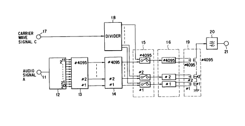
An embodiment of the invention will be explained
with reference to the circuit shown in FIG. 2.
Reference 11 denotes an input terminal for
receiving a audio signal A. The audio signal A inputted
to the input terminal 11 is applied to an A/D converter
12, where it is converted to a digital signal of, for
example, 12 bits, indicated by the binary number system
t2, 21, 22, ... 211). All the bits of the digital
signal are applied to a code unit 13 in a parallel
manner.
A code unit 13 has 4095 output terminals (#1 -
#4095) corresponding to the 12-bit binary signal, and
outputs a bit signal of "1" from one of the output
terminals determined by the bit value of the bit signal.
For example, when the value of "2" bit is 1 (i.e.
when the value is 1 in the decimal number system), "1"
is outputted to a bit signal output terminal of #1.
When the value of "21" bit is 1 (i.e., when the value is
~,_, 2128588
2 in the decimal number system), "1" is outputted to two
output terminals of #2 and #3. Further, when the value
of "22" bit is 1 (i.e., when the value is 4 in the
decimal number system), "1" is outputted to four output
terminals of #4, #5, #6 and #7.
In other words, the code unit 13 outputs "1" from
output terminals with smaller # numbers when the level
of a audio signal is low, and outputs "1" from both
output terminals with larger # numbers and those with
smaller # numbers when the level of the audio signal is
high.
The bit signals outputted from the output terminals
#1 - #4095 of the code unit 13 are supplied to the input
terminals (#l - #4095) of a code shifter 14,
respectively. The converter 14 has output terminals
(#1 - #4095) corresponding to the input terminals, and
has a function for periodically shifting or selecting at
random the destination of an input signal from each
input terminal. The operation of the code shifter 14
will be explained in detail later.
Each signal from the output terminals (#1 - #4095)
of the code shifter 14 is supplied as a switch control
signal to a corresponding one of 4095 carrier wave
switches (#l - #4095) 15.
Reference numeral 17 denotes an input terminal for
receiving a carrier wave signal C. The carrier wave
signal C supplied to the input terminal 17 is divided
~ 2128588
into 4095 portions by a carrier wave divider 18 and
supplied to the carrier wave switches (#l - #4095) 15,
respectively.
Each carrier wave switch 15 is electrically
conductive when the switch control signal from the code
unit 13 is "1", and nonconductive when the switch
control signal is "0", thereby selectively receiving
divided portions of the carrier wave signal C. Each of
the received portions of the signal C is amplified
by a corresponding one of 4095 power amplifiers 16
(#1 - #4095) with a predetermined gain, and then
supplied to a carrier wave combiner 19.
The carrier wave combiner 19 has 4095 transformers
(#1 - #4095). The primary winding of each transformer
is connected to the output terminal of a corresponding
one of the 4095 power amplifiers 16, and the secondary
windings of the transformers are connected to one
another in series. One end of the connected secondary
windings is grounded, and the other end is used as an
output terminal.
In the carrier wave combiner 19 constructed as
above, when those portions of the carrier wave signal C
which have been amplified by the power amplifiers 16
(#1 - #4095) are supplied to corresponding ones of the
primary windings, they are combined and digitally
summed up on the side of the secondary windings. A
combined output is generated from the secondary
~ 2128~88
-- 10 --
windings, and is outputted as an amplitude modulated
wave signal AM from an output terminal 21 after an
unnecessary high frequency component of the combined
output is removed by a bandpass filter 20.
The structure and operation of the power amplifier
16 is described in detail in USP 4,580,111, and hence no
detalled explanations will be given thereof.
The operation of the circuit comprising the
elements 12 - 16 will be explained with reference to
FIG. 3. In FIG. 3, elements similar to those shown in
FIG. 2 are denoted by corresponding reference numerals.
Further, although in the case of FIG. 2, the audio
signal A is converted to a 12-bit digital signal, the
signal is converted to a 4-bit (2, 21, 22, 23) digital
s$gnal in FIG. 3, for easy understanding.
The audio signal A supplied to the input terminal
11 is converted to a 4-bit digital signal by the A/D
converter 12, which has four output terminals (#1 - #4)
connected to the input terminals (#l - #4) of the code
unit 13, respectively.
The code unit 13 has four input terminals (#1 - #4)
and fifteen output terminals (#1 - #15). The input
terminal #l connected to the 2-bit output terminal of
the A/D converter 12 is connected to the output terminal
#1 via a buffer amplifier B1; the input terminal #2
connected to the 21-bit output terminal is connected to
the output terminals #2 and #3 via buffer amplifiers B2
212&588
and s3, respectively; the input terminal #3 connected to
the 22-bit output terminal is connected to the output
terminals #4 - #7 via buffer amplifiers s4 - s7,
respectively; and the input terminal #4 connected to the
23-bit output terminal is connected to the output
terminals #8 - #15 via buffer amplifiers s8 - B15,
respectively. Thus, a number of signals of "1"
corresponding to the number indicated by 4-bit data from
the A/D converter 12 appear at the output terminals
#1 - #15.
The fifteen output terminals #l - #lS of the code
unit 13 are connected to the fifteen input terminals
1 - #15) of the code shifter 14, respectively.
The code shifter 14 has a matrix type switch SW
consisting of (15 x 15) switch elements arranged at the
intersecting points of input/output lines (#l - #15)
such that they connect the intersecting points. The
input terminals #1 - #15 of the converter 14 are
connected to the input lines of the switch SW, while the
output terminals #1 - #15 are connected to the output
lines of the switch SW.
The above matrix type switch SW can easily be
realized by a logic IC, etc. The switching can be
controlled by a switch control section (not shown) such
that each input line is connected to an output line with
a corresponding # number in an initial state, and is
successively switched to other output lines in the order
2128588
- 12 -
of # number, each time a clock generator CL raises a
clock pulse of a predetermined frequency.
Specifically, at a certain point of time (t = n),
intersecting points indicated by circles are connected.
At a point of time (t = n+l) after a predetermined time
(here, one clock) from the time point (t = n)~
intersecting points indicated by squares are connected.
Further, at a point of time (t = n+2) after the
predetermined time from the time point (t = n+l),
intersecting points indicated by triangles are
connected.
Thus, in the FIG. 3 embodiment, the on-state
intersecting point shifts to the right (the rightmost
point shifts to the leftmost point) each time a clock
pulse rises. The input terminal #1, for example, is
successively connected to the output terminals #1, #2,
#3, ..., in this order with the lapse of time.
Similarly, the input terminal #2 is successively
connected to the output terminals #2, #3, #4, ..., in
this order with the lapse of time.
The output terminals #1 - #15 of the code shifter
are connected to control input terminals corresponding
to the carrier wave switches (#l - #15) 15,
respectively. Each of the switches 15 is in the on-
state when "1" has been applied thereto from a
corresponding output terminal of the code shifter 14.
As was explained referring to FIG. 2, the carrler wave
~ 2128~88
- 13 -
signal C is applied to the power amplifiers (#1 - #15)
16 via the on-state carrier wave switches (#1 - #15) 15,
thereby turning on the power amplifiers 16.
Thus, in the FIG. 2 embodiment having a structure
as shown in FIG. 3, even when audio signals A of the
same level are applied, and signals are outputted from
the same output terminal of the code unit 13, the switch
elements of the matrix-type switch SW are switched from
one to another each time a predetermined period of time
elapses, and hence the on-state carrier wave switches 15
are shifted from one to another with the lapse of time.
In other words, even when no level changes are found in
the inputted audio signals A, there are no power
amplifiers which operate concentratedly.
In particular, even when a audio signal A of a low
level has been generated, the matrix type switch SW
enables the uniform frequency of use of the power
amplifiers 16 with both smaller numbers and larger
numbers. Accordingly, the amplifiers 16 can each have
uniform reliability, and the reliability of the overall
system can be enhanced.
Further, increasing the frequency of the clock
pulses increases the speed of switching the intersecting
switch elements of the switch SW from one to another,
and thus more equalizes the heating value of each power
amplifier, with the result that the heating value of the
overall system can be reduced.
'- 212~8
- 14 -
Here, the heating value of the power amplifiers,
obtained in the conventional case shown in FIG. 1 will
be compared with that of the power amplifiers, obtained
in the present case shown in FIG. 2. Since the heating
value of the power amplifiers is proportional to the
average output power of the power amplifiers, the
average output power is used for the comparison.
In the conventional case, when the degree of
modulation is 0%, a particular power amplifier is
operated and generates heat. For example, if the
transmitter has an output of 1 kW and the margin of peak
modulation is 110%, the output power Pl of that one of
the power amplifiers which is operated under no
modulation conditions is given by
Pl = the average power of the transmitter/the
number of power amplifiers being operated
= 1000 W/((15 x 1.1)/2)
= 1000/6.815 = 147 W ... (1)
In the case of the present invention, all the power
amplifiers are operated in a uniform manner, and
therefore the output power P2 of each amplifier is given
by
P2 = 1000 W/15 = 67 W ... (2)
Further, when the transmitter is under rated
conditions or program modulation conditions (the degree
of modulation is 40 %), the average output of the
transmitter is 1.08 times of that obtained under no
~- 2128~88
modulation conditions. Accordingly, the output power P3
of each power amplifier is given by
P3 = 1000 W x 1.08/15 = 72 W ... (3)
As is evident from equations (1) - (3), the heating
value of each power amplifier is half or less of that
obtained in the conventional case. As a result, the
reliability of the system can be enhanced, the design of
a radiator system be simplified, the total efficiency be
increased, and the cost be reduced.
Although in the above code shifter 14, the
intersecting points which connect the input terminal of
the switch SW to the output terminal of the same are
simultaneously shifted from some to others at regular
intervals, the time points at which the shifting is
performed can be partially changed. Moreover, the
manner of shifting may be modified such that the fifteen
intersecting points are divided into five groups each
consisting of three intersecting points, and the
shifting is performed in units of a group. In this
case, too, the power loss of each power amplifier 16 can
be substantially uniformed.
Although the operation of the 4-bit code shifter 14
has been explained, the operation of the 12-bit
converter shown in FIG. 2 can be explained in a similar
manner. Further, although in the embodiment, all bit
conversion is performed by the converter 14, it is
practically no problem to sub;ect, in the 12 bit case,
2 1 2 8 ~ 8 8
- 16 -
for example, only the upper 4 bits to code conversion,
in view of the fact that "1" is generated relatively
often with respect to lower bits.
Another embodiment of the invention will now be
explained with reference to the block circuit diagram of
FIG. 4. In the FIG. 4 embodiment, elements similar to
those of FIG. 2 are denoted by corresponding reference
numerals, and no detailed explanations will be given
thereof.
In FIG. 4, the audio signal A inputted to the
input terminal 11 is applied to the A/D converter 12,
and converted to a 12-bit digital signal (2, 21, 22,
... 211) indicated by the binary number system. The
lower bits (2 - 27) of the digital signal are converted
to analog bit signals by a D/A converter 22, and
supplied to an analog power amplifier 23. A carrier
wave signal C is supplied directly to the analog power
amplifier 23 via the input terminal 17 and the divider
18. The carrier wave signal C is amplified in
accordance with the level of analog bit signals applied
from the D/A converter 22.
On the other hand, the upper bits (28 - 211) of the
digital signal are applied to the carrier wave switches
(#1 - #15) 15 via a variable code unit 14a, and
processed in a manner similar to that employed in the
FIG. 3 embodiment.
The portions of the carrier wave signal which have
~ 2128S88
- 17 -
been amplified by the power amplifiers (#l - #15) 16 and
the analog power amplifier 23, respectively are
combined by the carrier wave combiner 19 having
#0 - #15 transformers, and outputted as an amplitude
modulation wave signal from the output terminal 21
through the bandpass filter 20.
At present, in the medium wave hand, for example, a
power amplifier of a m~ n i mllm structure can output a
power of about 1 kW. Thus, a transmitter of an output
of 5 - 10 kW can be realized by employing 15 power
amplifiers (corresponding to 4 bits).
In the FIG. 4 embodiment, the power amplifier unit
comprises fifteen power amplifiers 16 and one analog
power amplifier 23, and hence it is necessary to divide
the carrier wave signal into sixteen portions by the
dlvider 18.
The operation of the above-described embodiment
will be explained. Since, as aforementioned, "1" is
relatively often generated with respect to any of lower
bits, it is practically no problem to subject only the
upper 4 bits to code conversion in the 12 bit case, for
example. Therefore, in the FIG. 4 embodiment, the lower
bits (2 - 27) of the digital signal are amplified by
analog processing, thereby decreasing the number of the
power amplifiers and accordingly reducing the cost.
Further embodiments of the invention will be
explained with reference to the block circuit diagrams
~- 2i2~588
- 18 -
of FIGS. 5 and 6. In these figures, elements similar to
those shown in FIGS. 2 and 4 are denoted by correspond-
ing reference numerals, and no detailed explanations
will be given thereof.
Although in the FIG. 2 embodiment, the code unit 13
and the code shifter 14 are formed of different circuit
blocks, in the FIG. 5 embodiment, the code unit 13 and
the code shifter 14 are formed integral of a single
circuit block sl. Similarly, although in the FIG. 4
embodiment, the code unit 13a and the code shifter 14a
are formed of different circuit blocks, in the FIG. 6
embodiment, they are formed integral of a single circuit
block B2.
Specifically, in the embodiment shown in FIG. 2 or
4, a digital signal corresponding to the audio signal A
is converted to an output indicated by number determined
by the digital value thereof in the code unit 13 or 13a,
and then a switch control signal for selecting a power
amplifier to be operated on the basis of the output of
the code unit is created in the code shifter 14 or 14a.
On the other hand, in the embodiment shown in
FIG. 5 or 6, the code unit 13 or 13a and the code
shifter 14 or 14a are formed integral as one block
circuit, where a digital signal used for encoding is
subjected to software processing or DSP (digital
processing IC) processing so as to create a switch
control signal for determining a power amplifier to be
~ 2128~88
- 19 -
operated.
An EP-ROM tErasable Programmable Read Only Memory)
can be used to form a circuit serving as both the code
unit and the code shifter.
FIG. 7 is a block circuit diagram, showing the case
of using an EP-ROM as the circuit block Bl of FIG. 5.
In FIG. 7, elements similar to those shown in FIG. 5
are denoted by corresponding reference numerals, and no
detailed explanations will be given thereof. In
addition, as in the FIG. 3 embodiment, the A/D converter
12 converts the audio signal A to a 4-bit (2, 21, 22,
23) digital signal, for easy understanding.
In FIG. 7, the circuit block Bl constituting the
code unit and the code shifter has an EP-ROM sll, a
clock generator B12 and a qulndecimal counter B13.
The clock generator B12 generates a series of clock
pulses at the time points shown in FIG. 8A. The clock
signal is added to the quindecimal counter B13, where it
is converted to a quindecimal signal.
The quindecimal counter sl3 has four bit terminals
(bit 0 - bit 3). A signal as shown in FIG. 8E is
generated from the bit-0 terminal, a signal as shown in
FIG. 8D is generated from the bit-l terminal, a signal
as shown in FIG. 8C is generated from the bit- 2
terminal, and a signal as shown in FIG. 8B is generated
from the bit-3 terminal. Hereinafter, the high level of
the output of each bit terminal of the quindecimal
2128~88
- 20 -
counter B13 is indicated by "1", and the low level of
the same is indicated by "0".
The outputs of the four bit terminals of the
quindecimal counter B13 are supplied to input terminals
A0 - A3 of the EP-ROM Bll, respectively. The audio
signal A applied to the input terminal 11 is converted
to a digital signal of 4 bits (2o, 21, 22, 23) by the
A/D converter 12. Thus, the A/D converter 12 has four
output terminals (#l - #4) connected to input terminals
A4 - A7 of the EP-ROM Bll.
Although the EP-ROM Bll has sixteen input terminals
and sixteen output terminals, eight input terminals A0 -
A7 and fifteen output terminals D0 - D14 are used in the
case of FIG. 7. Here, note that the EP-ROM Bll is an
element wherein the combination of output terminals from
which output signal are generated is determined directly
by the combination of input terminals supplied with
input signals. In this embodiment, the combinations of
input signals and output signals are set, for example,
as shown in FIG. 9.
FIG. 9 shows a part of combinations, wherein A0 -
A7 in the east-west direction correspond to the input
terminals A0 - A7 of the EP-ROM Bll, and D0 - Dl4 in the
same direction correspond to the output terminals. The
values in the north-south direction are count values of
the quindecimal counter B13, which repeats from 0 to 14.
In other words, FIG. 9 indicates which of the
~_ 2128~8
- 21 -
output term~ ~Al S DO - Dl4 of the EP-ROM Bll generate
signals, on the basis of the combination of the output
of each of the four bit terminals of the quindecimal
counter B13 and the bits of the digitized audio signal
A. AS regards the output terminals D0 - D14, "l"
indicates that they generate an output signal.
If there is no digitized audio signal, i.e., if the
input terminals A4 - A7 receive no bit signals, the
output terminals D0 - Dl4 generate no signals
irrespective of the count value of the counter B13
(inputs to the input term~ n~l S A0 - A3).
If the 2 bit of the digital audio signal is at
active level, i.e., if the input terminal A4 receives a
bit signal, the output terminal D0 generates "1" when
the count value of the counter B13 is "0". In this
case, the larger the count value of the counter B13 is,
the further right-side located output terminal generates
"1" .
If the 21 bit of the digital audio signal is at
active level, i.e., if the input terminal A5 receives a
bit signal, two output terminals, e.g. Dl and D2,
generate "1" when the count value of the counter B13 is
"0". In this case, the larger the count value of the
counter B13 is, the further right-side located output
terminals generate "1" in units of two.
If the 22 bit of the digital audio signal is at
active level, i.e., if the input terminal A6 receives
~,_ 2128S88
- 22 -
a bit signal, four output terminals, e.g. D3 - D6,
generate "1" when the count value of the counter B13 iS
"o~. In this case, the larger the count value of the
counter B13 iS, the further right-side located output
terminals generate "1" in units of four.
Lastly, if the 23 bit of the digital audio signal
is at active level, i.e., if the input terminal A7
receives a bit signal, eight output terminals, e.g. D7 -
D14, generate "1" when the count value of the counter
B13 iS "0". In this case, the larger the count value of
the counter B13 iS, the further right-side located
output term~ n~l C generate "1" in units of eight.
Where a plurality of bits, e.g. 21 bit and 22 bit,
of the digital audio signal are at active level, it
should be considered that the state wherein the 21-bit
portion is in the on-state overlaps the state wherein
the 22 bit is at active level.
For example, when the count value of the counter
B13 is "0", two output terminals Dl and D2 generate "1"
in accordance with an input (corresponding to the 21
bit) to the input terminal A5, and four output terminals
D3 - D6 generate "1" in accordance with an input
(corresponding to the 22 bit) to the input terminal A6.
That is, six output terminals generate "1".
In this case, the larger the count value of the
counter B13 is, the further right-side located output
terminals generate "1" in units of six.
'- 2128588
- 23 -
As explained above, in the EP-ROM Bll, the output
terminal D0 - D14 from which a bit signal is generated
is determined directly from the combination of a bit
(2, 21, 22, 23) portion(s) of the digitized audio
signal and the count value of the quindecimal counter
B13.
The outputs of the EP-ROM Bll are applied to the
carrier wave switches (#l - #15) 15, thereby turning on
them. As a result, the carrier wave bit signals C are
applied to and amplified by the power amplifiers 16
(#1 - #15), as in the FIG. 2 case. The bit signals C
amplified by the amplifiers 16 are combined by the
carrier wave combiner 19, filtered by the band filter
20, and outputted as an amplitude modulation wave from
the output terminal 21.
In the above-described structure, even if audio
signals A inputted have the same level, the output
terminals from which signals are generated are changed
from one to another (or from some to others) with the
lapse of time in accordance with the count value of the
quindecimal counter B13. Accordingly, the power
amplifiers 16 to be used are changed with the lapse of
time even when audio signals have the same level, and
the concentrated use of a particular power amplifier is
prevented.
The combination of each bit ( 2, 21, 22, 23)
portion of the digitized audio signal and the count
~_ 2128588
- 24 -
values of the quindecimal counter B13 is not limited to
that shown in FIG. 9, but can be modified in various
manners. Although the above-described explanations have
been given of the 4-bit case, similar explanations can
be given of the 12-bit case.
Moreover, although in the above embodiments, all
the bits of a digitized audio signal are processed, the
invention is applicable also to the case of processing
only part of the bits, e.g. upper or lower bits, of the
digitized audio signal.