Note: Descriptions are shown in the official language in which they were submitted.
212~9~
PATENT
PD-93094
DIRECT MOMBE AND MOVPE GROWTH OF
II-VI MATERIALS ON SILICON
BACKGROUND OF THE INVENTION
1. Field of the Invention
The present invention relates to the deposition of II-
VI semiconductor films, and, more particularly, to the dep-
osition of ternary chalcogenide semiconductor films, such
as HgCdTe and HgZnTe, onto silicon substrates.
2. Description of Related Art
Ternary II-VI semiconductor films find use in many in-
fra-red (IR) applications, such as in IR focal plane arrays
(FPAs). Examples of such ternary II-VI semiconductor com-
pounds include HgCdTe and HgZnTe, which are also known as
chalcogenides.
The current size of HgCdTe focal plane arrays which
are fabricated from homoepitaxial material is limited to
64x64 pixels because of delamination problems with the sil-
icon readout to which the FPA is bonded by indium bump
technology. The delamination problem is a consequence of
the large thermal expansion mismatch between silicon and
the CdZnTe substrate on which the active HgCdTe layers are
grown.
Direct growth of HgCdTe on silicon not only accommo-
dates this mismatch by forcing the FPA to expand and con-
tract with the silicon substrate but allows HgCdTe growth
on large area high quality substrates which are not avail-
able for homoepitaxy. Direct growth of HgCdTe on silicon
is difficult, however, due to the large lattice mismatch
21 28590
(approximately 20S) and the polar versus nonpolar nature of
HgCdTe versus silicon.
Buffer layers of ZnSe (4% lattice mismatch with sili-
con) and ZnTe (8% lattice mismatch with silicon) can be
grown to step grade th- tran ition to HgCdT-, but direct
growth of these material~ on silicon also yield~ poor qual-
ity or polycrystalline film~.
Recently, it has been reported that high quality lay-
ers of ZnSe can b~ grown on silicon by molecular bea~ epi-
taxy (MBE) i~ the sil~con substrate i~ terminated by a lay-
er of arsenic atoms; ses, e.g., R.D. Bringan~ et al, M~te-
rials Rese~rch Society Sympos~ Proceedings, Vol. 2~2, pp.
191-202 (1992). It is hypothesized that the function of
arsenic is to pa~sivate th~ silicon surface by fully co-
ordinating the surface layer as well as providing an ini-
tial polarization of the surface for subsequent II-VI
growth.
The first demonstration o~ the MBE growth of ZnTe on
As-terminated silicon was recently the subject of U. S.
Patent No, 5,306,386, issued April 26, 1994, and
assigned to the same assignee as the present application.
Successful growth of ZnSe on Si terminated with a
monolayer of As (henceforth referred to as ZnSe//As:Si)
achieved by MBE, however, does not mean that the same
approach will bQ ~cce~sful in a metalorganic MBE (MOMBE)
environment. Due to the large background pressure of
organic radicals in the MOM~E environment generated by the
thermal pre-cracking of the metalorganic sources, it has
been believed that MOMBE growth on silicon would not be
possible. It is well-documented in the ~urfac- science
literature that hydrocarbon radicals, in particular methyl
radicals, irreversibly adsorb on silicon surface~ and de-
compose to form carbides on the surface when heated; see,
e.g., M.~. Colaianni et al, Che~ic~l Phys~cs Letters, Vol.
191, pp. 561-568 (17 April 1992). Studies have also shown
that organoarsenic sources will strongly interact with sur-
face oxides to leave carbonaceous contamination on the
21 2 ~ J ~) ~
growth surface; see, e.g., P. Kaul et al, Journal of Crys-
tal Growth, Vol. 123, pp. 411-422 (1992).
Simply adding a solid arsenic source to the MOMBE
growth chamber is not the best solution, as the compatibil-
ity of solid sources in a metalorganic environment is not
established. Accordingly, a method is needed for the for-
mation of a monolayer of arsenic on silicon substrates us-
ing MOMBE.
Similar considerations also apply for the deposition
of arsenic on silicon substrates using other metalorganic
deposition procedures. An example of such other deposition
procedure is MOVPE (metalorganic vapor phase epitaxy), also
known as MOCVD (metalorganic chemical vapor deposition),
which is carried out under vacuum conditions not as high as
lS those employed in MOMBE. For example, the base pressure
after bakeout for MOMBE will be ultrahigh vacuum (101~ to
10-11 Torr) MOVPE chambers are not baked and have base
pressures more typically on the order of 104 to 107 Torr,
depending on how they are pumped.
Thus, a need remains for the epitaxial growth of good
quality binary and ternary II-VI semiconductor films on a
silicon substrate.
SUMMARY OF THE INVENTION
In accordance with the invention, a metalorganic ar-
senic source is provided that can terminate a silicon sur-
face with a monolayer of arsenic without carbon contami-
nation and permit subsequent growth of high quality ZnSe
thereon. Use of such a metalorganic arsenic source allows
the full potential of the MOMBE technique, which has dem-
onstrated superior flux control than that achieved by MBE,
to be realized in the heteroepitaxy of HgCdTe on silicon
substrates. Further, the metalorganic arsenic source can
be used in other metalorganic deposition procedures, such
as MOVPE.
21 28590
The method of the invention employs a~ the metalor-
ganic arsenic source a compound of the formula R3_mAsH~,
where R is an organic radical selected from the group con-
sisting of CnH2n~1 and CnH2n-1~ where n ranges from 1 to 6,
and where m is 1 or 2.
The arsenic metalorganic compound is used in vacuum
deposition processes in which the ratio of reagent (metal-
organic compound) pressure to background pressure is advan-
tageously at least about lOO:l.
The method of the invention comprise~ exposing a sili-
con substrate having an appropriately cleaned and hydrogen-
terminated surface to the arsenic metalorganic source and
monitoring the nature of the surface by reflection high-
energy electron diffraction (RHEED) analysis. Specifical-
ly, during the deposition, the RHEED intensity initially
increases. Once the RHEED intensity stops increasing, or
saturates, the silicon surface is passivated with arsenic
and the ilicon wafer can then be further procosr~~ for
growth of the II-VI layer on the arsenic-terminated sur-
face.
The arsenic metalorganic source employed in the methodof the invention provides a monolayer of arsenic on the
silicon surface without carbon contamination of the sur-
face.
Other aspects of this invention are as follows:
A method of passivating a surface of a silicon sub-
strate with an arsenic film, comprising:
(a) placing said silicon substrate in a vacuum
growth chamber adapted for growth of films from metalorgan-
ic compounds and having a ratio of compound pressure tobackground pressure of at least 100:1; and
(b) exposing said silicon substrate to vapors
from an arsenic metalorganic compound having the formula
R3_mAsHm, where R is an organic radical selected from the
group consisting of CnH2n+l and CnH2n_l, where n ranges from
1 to 6, and where m is 1 or 2, for a period of time to
ensure passivation of said surface.
,:;. I~'
21 28590
4a
A method of growing a layer of a II-VI semiconduc-
tor compound on a surface of a silicon substrate, compris-
ing:
(a) passivating said surface in accordance with
the method of Claim 1; and
(b) growing said II-VI semiconductor film on said
arsenic-passivated surface.
BRIEF DESCRIPTION OF THE DRAWINGS
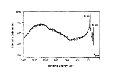
FIG. 1, on coordinates of intensity (in arbitrary
units) and binding energy (in eV), is an X-ray photoelec-
tron spectroscopy (XPS) spectrum (Al KQ excitation, Fixed
Retard Ratio (FRR) 5 analyzer mode, 15 KV, 20 ma) of a sil-
icon substrate, prepared by a dip in 4.5% HF, prior to ex-
posure to t-butylarsine;
FIGS. 2a and 2b, on coordinates of intensity (in ar-
bitrary units) and binding energy (in eV), are high reso-
lution XPS spectra taken in Fixed Analyzer Transmission
(FAT) mode with a pass energy of 2S eV, with Al K~ excita-
,
. i . .
5 212~ ~.J ~ ~
tion (15 KV, 20 ma) of As 3d electrons (FIG. 2a) and C ls
electrons (FIG. 2b) regions following exposure of a silicon
substrate to t-butylarsine during temperature ramp of the
substrate;
FIG. 3, on coordinates of intensity (in arbitrary
units) and theta angle (in degrees), is a plot of double
crystal X-ray rocking curves for (001) ZnSe films grown on
silicon with and without arsenic passivation from t-butyl-
arsine.
DESCRIPTION OF THE PREFERRED EMBODIMENTS
The present invention details a method whereby high
quality layers of II-VI materials can be grown by MOMBE
directly on silicon substrates. This has been achieved by
using an arsenic metalorganic compound of the formula R3_m~
AsHm, where R is an organic radical selected from the group
consisting ~f CnH2n+1 and CnH2n_l, where n ranges from 1 to
6, and where m is 1 or 2. Preferably, n is at least 2.
Examples of metalorganic arsenic compounds useful in
the practice of the invention broadly include CnH2n+lAsH2,
CnH2n-1ASH2~ (CnH2n+l)2AsH~ and (CnH2n_1)2AsH. More specific
examples include tertiary-butyl arsine, isopropyl arsine,
ethyl arsine, neopentyl arsine, cyclohexyl arsine, allyl
arsine, and vinyl arsine.
Such arsenic metalorganic compounds as defined above
may be used to terminate the silicon substrate with a layer
of arsenic atoms prior to the initiation of II-VI growth.
In particular, the use of tert-butyl arsine (t-BuAsH2) for
passivating the silicon surface is the first demonstration
that an organometallic source can be used to terminate a
silicon surface with arsenic without carbon contamination
of the surface which would lead to defects at the interface
and degradation of the subsequent epilayer. The ability to
use an all-metalorganic approach avoids the problems asso-
ciated with carbon contamination of solid sources installed
in otherwise metalorganic systems. Contamination of solid
6 ~ ~ 2 ~ 0
sources by carbonaceous deposits can change the character-
istics of the solid source flux and composition in an un-
controllable and irreproducible way.
The inventors are not aware of any other method by
which direct growth of II-VI materials on silicon by MOMBE
has been demonstrated. In general, the MOMBE growth tech-
nique offers superior flux control without flux transients
and without crucible depletion effects which are inherent
in MBE. The rapid and reproducible flux control of MOMBE
allows facile determination of growth kinetics and surface
phase diagrams which are valuable tools in optimizing film
quality.
The inventors have developed a method by which MOMBE
growth on silicon can be achieved using t-BuAsH2 to termi-
nate the silicon surface with arsenic and have demonstrated
the growth of crystalline ZnSe using this technique. t-Bu-
AsH2 is a compound which consists of arsenic bound to two
hydrogens and a tertiary-butyl group (-C(CH3)3). Although
the exact mechanism of decomposition is unknown, it is be-
lieved that the presence of the hydrogen ligands lead to
efficient recombination of the tertiary-butyl radical with
hydrogen to form a stable hydrocarbon which has less pro-
pensity to dissociatively adsorb on the silicon surface.
Other hydrocarbon radicals R, given by the formula
CnH2n+1 or CnH2n_l, where n ranges from 1 to 6, may also be
employed in the practice of the invention, so long as they
form stable hydrocarbons during the decomposition of the
metalorganic compound on the silicon surface. Preferably,
n ranges from 2 to 6, and most preferably, is a sterically-
hindered radical, such as t-butyl, isopropyl, neopentyl,
and cyclohexyl. Other radicals also useful in the practice
of the invention include ethyl, allyl, and vinyl.
As an example of the method of the invention, a sili-
con wafer is provided with a pre-cleaned, hydrogen-pas-
sivated surface. The pre-cleaning is accomplished using
the well-known RCA cleaning procedure, which comprises
first degreasing the silicon wafer and then exposing the
2 ~ 2 3 J n 3
silicon surface to an etchant comprising an aqueous solu-
tion of hydrogen peroxide and ammonium hydroxide. This
pre-cleaning procedure improves the morphology of the final
II-VI layer.
5Hydrogen passivation of silicon surfaces is well-known
in the art and is achieved by a dip in dilute aqueous HF
solution, e.g., 4.5% HF. The pre-cleaned, hydrogen-pas-
sivated silicon wafer is then placed in the growth chamber.
The silicon wafer is outgassed for a time sufficient
10to desorb any hydrocarbons adsorbed on the silicon surface.
Typically, the outgassing process is carried out at a tem-
perature of about 150~C for about 1 hour.
The metalorganic source cell (also known as the crack-
er cell) in the MOMBE apparatus may be heated to an elevat-
15ed temperature of about 150~C. The temperature is selected
to be high enough to prevent condensation of water vapor in
the cell which is water-cooled but low enough to prevent
dissociation of the metalorganic in the cell itself, as it
is desired that the metalorganic be cracked on the silicon
20surface. The other cells of the MOMBE apparatus are also
heated to a temperature of about 150~C. This keeps water
from condensing on them and keeps the background pressure
low. It will be appreciated that the temperature of 150~C
is not critical, and other elevated temperatures that
25accomplish the same purposes may be used.
The background pressure of the MOMBE apparatus is
maintained at about 5xlO-9 to lx10-8 torr, and the cryopan-
els are cooled using liquid nitrogen.
The silicon wafer is exposed to the arsenic metalor-
30ganic compound. An upstream pressure of about o.g torr of
the arsenic metalorganic compound is typically used, but
this may range from about 0.1 to 10 Torr. This is done by
flowing the gaseous compound through an orifice of about
0.5 mm, but which may range in size from about 0.3 to 4 mm.
35The growth chamber pressure is about 4x10⁻⁷ Torr, but may
range in pressure from about 10 8 to 10-4 Torr. The im-
portant parameter in the metalorganic As exposure is the
2 ~ D
ratio of the As beam to ambient background. The same ratio
may be obtained with different combinations of orifice
sizes and upstream pressures which will in turn affect the
operating pressure. That is why the ranges given are so
broad.
It is preferred that the ratio of metalorganic As beam
pressure to background pressure be at least about 100:1.
Lower ratios may be used; however, the driving consider-
ation here is the relative sticking coefficient of arsenic
compared with that of the background materials (such as
hydrocarbons and water). A ratio of at least about 100:1
has been successfully used to ensure that the arsenic film
deposited on the silicon surface is essentially arsenic,
although a lower ratio may also be employed.
When the flux from the source material (arsenic
metalorganic compound) is stable, the substrate temperature
is increased to at least 500~C. This a consequence of pri-
or HF dip used to prepare the silicon surface, which leaves
the surface with a hydrogen-termination. This hydrogen
does not begin to desorb from the silicon surface until
about 500~C. At this temperature, the t-BuAsH2 will also
decompose on the surface. Prior to the adsorption of As,
the (100) Si surface has a structure representative of a
bulk termination i.e. (lxl) as determined by RHEED. Follow-
ing As adsorption on the Si surface, the RHEED pattern
changes to a double periodicity in a single [110] direction
i.e. a (2xl) reconstruction of the surface occurs.
The RHEED pattern is monitored by measuring the inten-
sity of diffracted electrons in the specular direction dur-
ing 4he arsenic deposition. When the intensity no longer
increases, the silicon surface is assumed to be passivated.
This measured time interval is increased by a factor of
about 3 to 6 during the exposure to ensure that passivation
is complete.
3S It takes about 5 minutes to achieve a substantially
constant intensity. Typically, the silicon surface is ex-
posed for about 15 to 30 minutes, or about 3 to 6 times the
2 ~ 3 ~
minimum time required to passivate the surface. Once the
surface is passivated, the arsenic metalorganic source is
shuttered off from the system. The temperature of the As-
passivated silicon wafer is then lowered to the appropriate
growth temperature for growth of the II-VI layer. The de-
tails of such II-VI growth are conventional and do not form
a part of this invention.
As indicated above, the teachings of the invention can
be incorporated in other metalorganic deposition processes,
including MOVPE. Arsenic passivates the silicon surface
and provides an improved growth layer for subsequent II-VI
growth. This advantage appears to be due to the fact that
arsenic is more ionic than silicon, which is covalent, and
thus possesses an ionic nature that is more similar to that
of the II-VI compound than does silicon.
The MOVPE process also begins with a silicon wafer
which has a hydrogen-passivated surface obtained by a dip
in dilute HF. Similarly, the hydrogen-passivated surface
is placed in the MOVPE chamber and outgassed at a tempera-
ture of 150~C for about 1 hour, but this is done in thepresence of flowing molecular hydrogen with a flow rate
which may span from 1 to 10 liter per minute (lpm). Fol-
lowing this outgassing procedure, the surface is exposed to
flowing t-BuAsH2 at a flow rate which will allow the ratio
of the t-BuAsH2 pressure to background to be as high as
practically possible for the apparatus. This value may be
adjusted to allow a steady state t-BuAsH2 partial pressure
of 10 to 100 Torr. During the t-BuAsH2 exposure, the tem-
perature of the silicon wafer is raised to at least 500~C
and held there for the same length of time as in the MOMB~
case, i.eO, 15 to 30 minutes. At the end of this time, the
surface is assumed passivated and the normal procedure for
II-VI epilayer growth can be performed.
2~2~ O
EXAMPLES
Example 1:
In this Example, arsenic passivation in a MOMBE appa-
ratus is described. While in this Example the orientationof the silicon substrate was (001), other orientations,
such as (110) and (111), may also be employed in the prac-
tice of the invention.
Two-inch silicon substrates, either exactly oriented
(001) or oriented (100) and miscut either 4~ or 8O toward
the nearest <111> plane, were prepared by dipping in ap-
proximately 4% aqueous HF for approximately 15 seconds in
accordance with the method described by B.S. Meyerson et
al, Applied Physics Letters, Vol. 57, pp. 1034-1036 (1990).
The substrates were mounted on 2-inch molybdenum holders
designed for radiative heating and transferred into vacuum
within 15 minutes. X-ray photoelectron spectroscopy (XPS)
analysis of the silicon surfaces treated in this way indi-
cated that the silicon surface was free of carbon and oxy-
gen contamination as shown in FIG. 1.
The substrate was then transferred into the MOMBEchamber in which all gas source cell crackers were main-
tained at an indicated temperature of 200~C and the cryo-
panel was cold (liquid N2 temperature). It is important to
note that the cells are always maintained at this tempera-
ture when they are not in use to prevent residual water ad-
sorption. The reflection high energy electron diffraction
(RHEED) pattern of the silicon substrate as transferred was
streaked in a (lxl) pattern with no visible reconstruction.
The flow of t-BuAsH2 (Air Products, electronic grade), es-
timated to be on the order of 1 sccm, was initiated prior
to heating of the silicon substrate. After initiation of
the t-BuAsH2 flux, the temperature of the silicon substrate
was increased while the RHEED specular intensity was moni-
tored. At a substrate temperature of approximately 450~C,the specular intensity began to increase dramatically. The
silicon substrate was then held at 500~C for 15 minutes,
212~5~0
11
after which a strong (2xl) reconstruction could be clearly
observed by RHEED. At this exposure temperature, excess As
desorbs from the surface, and the adsorption is self-limit-
ing at one monolayer of As coverage. XPS analysis of the
silicon surface following this treatment revealed the pres-
ence of arsenic on the surface but no detectable carbon, as
shown in FIG. 2.
Growth of ZnSe was initiated on the arsenic-terminated
silicon surface after stabilizing the substrate temperature
at 380~C. The source materials used for ZnSe growth were
diethylzinc (DEZn) and diethylselenium (DESe), which were
thermally pre-cracked at 800~C and 900~C, respectively.
The cracker cells were raised to their operating tempera-
tures only after arsenic termination of the silicon surface
was complete. X-ray rocking curve measurements for an ap-
proximately 3 ~m ZnSe film grown on (001) As:Si as de-
scribed above and a ZnSe film grown on (001) Si without
arsenic termination are displayed in FIG. 3. These films
were grown using the same temperature and flux conditions
(380~C, 2.0 Torr DESe, 1.25 Torr DEZn), but the growth
times for ZnSe//As:Si versus ZnSe//Si were 6 and 12 hours,
respectively, with nominally similar growth rates. Despite
the shorter growth time and consequently thinner epilayer,
the ZnSe//As:Si had significantly superior crystalline
quality, confirming the successful As termination of the
Si(001) surface using t-BuAsH2.
Example 2:
In this Example, arsenic passivation in a MOVPE ap-
paratus is described.
Silicon substrates, oriented (001), are prepared by
dipping in approximately 4% aqueous HF for approximately 15
seconds in accordance with the method described by B.S.
Meyerson et al, Applied Physics Letters, Vol. 57, pp. 1034-
1036 (1990). The substrates are mounted on molybdenum
holders designed for conductive heating and transferred in-
to vacuum within 15 minutes.
2 ~
12
The substrate is then transferred into the MOVPE cham-
ber. The hydrogen passivated surface is outgassed at a
temperature of 150~C for about 1 hour in the presence of
flowing molecular hydrogen with a flow rate which may span
S from 1 to 10 lpm. Following this outgassing procedure, the
surface is exposed to flowing t-BuAsH2 at a flow rate which
allows the ratio of the t-BuAsH2 pressure to background to
be as high as practically possible for the apparatus. This
value is adjusted to allow a steady state t-BuAsH2 partial
pressure of 10 to 100 Torr. During the t-BuAsH2 exposure,
the temperature of the silicon wafer is raised to at least
500~C and held there for 5 to 30 minutes. At the end of
this time, the surface is assumed passivated and the normal
procedure for II-VI epilayer growth is commenced.
Thus, there has been disclosed a method for passivat-
ing silicon surfaces with arsenic for the subsequent growth
of II-VI layers thereon. It will be readily apparent to
those skilled in this art that various changes and modifi-
cations of an obvious nature may be made, and all suchchanges and modifications are considered to fall within the
scope of the invention, as defined by the appended claims.