Note: Descriptions are shown in the official language in which they were submitted.
2l2~n7~ ,
TITLE OF THE INVENTION
SEMICONDUCTOR OPTICAL DEVICE WITH MESA STRUCTURE WHICH IS
SURROUNDED LATERALLY BY INSULATING MASK FOR PREVENTING
CURRENT FROM LEAKING DIRECTLY FROM CLADDING LAYER TO
SUBSTRATE AND PROCESS OF FABRICATION THEREOF
FIELD OF THE INVENTION
This invention relates to a semiconductor optical ;
device and, more particularly, to a semiconductor optical ;~
device which is fabricated by selective MOVPE technique and
its fabrication process.
- DESCRIPTION OF THE RELATED ART
In the selective MOVPE, two stripe masks with a
center spacing is first patterned on a surface of a
semiconductor substrate. The center spacing is by way of
example, 2 microns. On the exposed center spacing
between the stripe is epitaxially grown a semiconductor
masks mesa structure including an active layer, a wave-
guide layer or an optical absorbing layer. This selective
MOVPE technique has better reproducibility in forming mesa
structure than conventional fabrication technique which
employs semiconductor etching.
The composition of the epitaxially grown
semiconductor material varies depending on the stripe mask
width, and this phenomenon is available for changing the
' ' ' :, '' ' '' ~ ' ': ' . ' ' '~- : ~ ' :
' , ' '':, " ~ ~ `''
''' ~ ' ' '
' - '' '' ' ' ' ~ ' : , : ' ~ . ,
212~Q7~
energy band gap in the mesa structure. This technology is
called as "band-gap controlling technology".
The following papers report semiconductor optical
devices fabricated through the selectively growing
technique.
(1) "Tunable DBR Laser Diodes with selectively Grown
Waveguide" reported by Tatsuya SASAKI et al, C-134,
Proceedings of 1991 Autumn Meeting of Electronic
Information Communication Society.
(2) Japanese Patent Publication of Unexamined
Application No. 5-37092.
(3) "Novel MQW-DFB-LD/ Modulator Integrated Light
Source" reported by Tomoaki KATO et al, C-133, Proceedings
of 1991 Autumn Meeting of Electronic Information
Communication Society.
Sasaki et al disclose three-terminal variable
wavelength DBR laser diodes, and the band-gap controlling
technology is available for simultaneously growing an
active layer and a passive wave guid~ of the three-terminal
variable wavelength DBR laser diode. The entire surface of
the structure is covered with a cladding layer. Sasaki et
al achieved the light output power 15 mill-watt around 1.55
micron wavelength with the three-terminal variable
~'
2~2~n7~
wavelength DBR laser diode, and the wavelength was varied
over 2.2 nano-meter band-width.
Kitamura discloses a semiconductor optical amplifier
or an LD amplifier in Japanese Patent Publication of
Unexamined Application No. 5-37092, and the selectively
growing technology is applied to patterning stage of the
active layer. The active layer is as narrow in width as
4000 angstroms, and is reproducible. Such a narrow active
layer is hardly patterned through the conventional etching
process. According to the Japanese Patent Publication of
Unexamined Application, the semiconductor optical amplifier
achieved the optical gain at 20 dB and a deflection
dependency, i.e., the deviation of the optical gain in
terms of deflection of incident light at 1.5 dB.
Kato et al reports an MQW-DFB-LD/modulator integrated
light ~ource, and the band-gap energy controlling
technology is applied to simultaneous growth of the active
layer and the light absorbing layer covered with the
cladding layer in the MQW-DFB-LD/modulator integrated light
source. The MQW-DFB-LD/modulator integrated light source
achieved a laser oscillation with the wavelength of 1.55
micron at the light output of 1.8 mill-watt, and the
extinction ratio was 22 dB at 2 volts. All of the
semiconductor optical devices discussed above are BH
. . . ~ - ,
,~ ~"~ ., ::,; ~ ........... ~ :,
~` .
.
, - . . :
. . : ~ ~
212J07~
structure where the light absorption layers, passive wave
guide layers or active layers are buried in semiconductor
materials.
Figures 1A to 1D illustrate the prior art process
sequence for fabricating a semiconductor laser oscillator,
a semiconductor light amplifier (or an LD amplifier) or a
light modulator, and the band-gap controlling technology is
incorporated in the prior art process sequence. In figures
1A to 1D, the cross section is perpendicular to [011]
orientation or the longitudinal direction of the
semiconductor optical device.
The prior art process sequence starts with an n-type
semiconductor substrate 1 of indium phosphide~ and (100)-
oriented surface serves as the major surface for the
optical device. On the major surface of the n-type
semiconductor substrate 1 is formed a stripe mask 2 of
silicon oxide which is 1000 angstroms in thickness and 10
microns in width. The stripe mask 2 is separated into two
parts 2a and 2b by a spacing and the spacing is 2 microns
wide.
Using the selective MOVPE technique, a buffer layer
3, an active layer 4 and a cladding layer are epitaxially
grown on the exposed spacing area and form a mesa stripe.
r`~
~: ......... . .. , :
21 2~74
The active layer 4 is indium gallium arsenide phosphide
layer of 1.55 micron wavelength composition, and is 2000
angstroms thick. The resultant structure of this stage is
illustrated in figure 1A.
The mask 2 on both sides of the mesa stripe is
partially removed so that the exposed area is spread on
both sides of the mesa stripe as shown in figure 1s.
The selective MOVPE technique is employed again, and
a cladding layer 6 and a cap layer 7 are grown over the
mesa stripe on the exposed area as shown in figure 1C. The
mesa stripe is buried in the cladding layer 6. The
cladding layer 6 is formed of p-type indium phosphide, and
is 1.5 micron thick. The cap layer 7 is formed of heavily
doped p-type indium gallium arsenide, and is 2000 angstroms
thick.
1000 angstroms thick silicon dioxide is deposited on,
and the silicon dioxide layer is partially removed so as to
expose the top surface of the cap layer 7. The silicon
dioxide layer and the mask 2 form passivation layer 8
covering the semiconductor optical device except for the
cap layer 7.
Finally, 4000 angstroms thick gold and 500 angstroms
thick titanium are deposited so as to form an electrode 9,
and the resultant structure of this stage is illustrated in
. . - :.. -
. ~
r~ :
2l2~n7~
figure 1D.
The substrate 1 of n-type indium phosphide and the
cladding layer 6 of p-type indium phosphide form a homo-
junction 10 therebetween. The substrate ; and the cladding
layer 6 at the homo-junction 10 are of the order of 5 x
1017 cm~3 in standard semiconductor optical devices.
If the electrode 9 is positively biased with respect
to the substrate 1, current flows from the electrode 9
through the cap layer 7, the cladding layer 6, the cladding
layer 5, the active layer 4, the buffer layer 3 into the
substrate 1, and the active layer 4 generates laser light.
If the substrate is the p-type, the cladding layers 5
and 6 and the cap layer 7 are doped with n-type dopant
impurity, and the buffer layer 3 is the p-type. As a
result, the current flows in the opposite direction.
The prior art process sequence is applicable to an
electroabsorption modulator which uses the Franz-Keldysh
effect, and the active layer 4 is replaced with a light
absorption layer.
The semiconductor optical device disclosed in the
paper (1) has a waveguide in serial to the active layer 4,
and the semiconductor optical device disclosed in the paper
(3) further has a light absorbing layer in serial to the
. . ~ .
. . .. . .. . .: -
212~374
active layer 4. These waveguide and the light absorbing
layer are formed through the band gap controlling
technology, and the stripe-shaped masks disclosed in the
papers (1) and 3 and the Japanese Pate~t Publication of
Unexamined Application are oriented to [011] direction.
The prior art semiconductor optical devices encounter
a problem in output characteristics. For example, the
prior art semiconductor laser oscillator hardly achieves
the light output exceeding 50 milli-watt, and the
semiconductor light amplifier can not achieve the light
output exceeding 25 dB. This is because of the fact that
the mesa-shaped structure is buried in the cladding layer
6, and the injected current partially flows across the
homo-junction directly between the cladding layer 6 and the
semiconductor substrate 1 without passing through the
active layer 4.
The prior art semiconductor light modulator is also
affected by the homo-junction 10. As described
hereinbefore, the standard doping level of the substrate 1
and the cladding layer 6 near the homo-junction are of the
order of 5 x 1017 cm~3. The total amount of parasitic
capacitance including the capacitance at the electrode 9 is
equal to or greater than 3 pF, and does not allow the
modulation bandwidth more than 2.4 GHz. In order to
. .
~' .. : ' , : . :
212~07~
achieve the band width 2.4 GHz, the total amount of
parasitic capacitance should be not greater than 2 pF.
Moreover, a problem is encountered in the prior art
process sequence in complexity. This is because of the
fact that the two selective MOVPE steps and the two mask
patterning steps are incorporated in the prior art process
sequence.
SUMMARY OF THE INVENTION
It is therefore an important object of the present
invention to provide a semiconductor optical device which
is improved in characteristics.
It is another important object of the present
invention to provide a process of fabricating a
semiconductor optical device which is less complex rather
than the prior art process sequence.
To accomplish the first object, the present invention
proposes to isolate a cladding layer 21 overlain by a cap
layer 22 from a semiconductor substrate 23 by an insulating
mas~ layer 24 laterally surrounding a mesa structure 25
including a buffer layer 26 and an active layer 27 as shown
in figure 2.
The present inventor fabricated the semiconductor
optical device shown in figure 2 through the prior art
, - . ~ :: . .
,i ~ , . :: . ~ . . :. .
!.' ` . . . ' ' . ~ :'
' '' , ~
212!~37~
selective MOVPE technology, the selective MOVPE technology
formed a cladding layer 21 a and a cap layer 22a having a
peak 28 as shown in figure 3. The present inventor
contemplated the undesirable peak 28, and concluded that
the insulating mask 24 oriented to [011] direction had
resulted in the undesirable peak 28. In detail, if a mesa
31 was selectively grown on a exposed center spacing 35a
between the insulating mask 33 which is oriented to [011]
direction, the mesa 31 firstly grew in a direction A
vertical to the major surface of the semiconductor
substrate 32, and had a flat top surface as shown in
figure 4A. However, the mesa 31 thereafter grew directions
inof B, and formed side surfaces 31b of (111) orientation
merged at the peak 34 as shown in figure 4B to 4D.
The peak 28 is not desirable, because an electrode
requires a flat top surface of the cap layer.
To accomplish the second ob ject, the present
invention proposes to decline an exposed center spacing at
least 5 degrees with respect to [011 ] direction. The
present inventor confirmed the effect of the present
invention. A semiconductor substrate 41 was exposed on the
spacing between the insulating mask 42 obliquely extending
at least 5 degrees with respect to [011] direction, a mesa
43 kept a trapezoid cross section through a selective MOVPE
.. . , .; , ... .
.: "' ,:. ., : .: ~ - : - - : .
. ..
.
212~`'J'~7~
as shown in figures 5A to 5C.
In accordance with one aspect of the present
invention, there is provided a semiconductor optical device
fabricated on a semiconductor substrate, comprising: a) an
insulating stripe mask with a exposed center spacing ; b) a
mesa structure grown on the center spacing so that the
insulating stripe mask is held in contact with a lower
portion of the mesa structure; c) a cladding and cap layer
grown from the mesa structure, and extending on an upper
surface of the insulating mask ; and d) electrode means for
supplying current through the cladding layer to the mesa
structure so that the mesa structure achieves an optical
fur.ction.
In accordance with another aspect of the present
invention, there is provided a process of fabricating a
semiconductor optical device, comprising the steps of: a)
preparing a semiconductor substrate having (100)
orientation surface; b) providing an insulating masks with
a stripe center spacing on the major surface, obliquely
extending at 5 degrees or more than 5 degrees with respect
to [011] direction of the crystal structure; c) forming a
mesa structure grown on the center spacing so that the
insulating masks are held in contact with a lower portion
J '.' ' . ` ' - . .
~"......... ' ~ .
212~7~
of the mesa structure; d) forming a cladding and cap layer
grown from the mesa structure and extending on an upper
surface of insulating mask, the cap layer having a flat top
surface; and e) forming an electrode electrically connected
to the cap layer for supplying current through the cladding
layer to the mesa structure.
BRIEF DESCRIPTION OF THE DRAWINGS
The features and advantages of the semiconductor
light device and the process of fabrication thereof
according to the present invention will be more clearly
understood from the following description taken in
conjunction with the accompanying drawings in which:
Figs. 1A to 1 D are cross sectional views showing the
prior art process sequence for controlling the band-gap in
the mesa structure;
Fig. 2 is a cross sectional view showing the
structure of a semiconductor optical device according to
the present invention;
Fiq. 3 is a cross sectional view showing the
structure of a semiconductor optical device fabricated
through the prior art process sequence;
Figs. 4A to 4D are cross sectional views showing the
mesa grown on the exposed center spacing between the
insulating masks oriented to [011] direction;
212 ~ 1) rl ~
Figs. 5A to 5C are cross sectional view showing the
mesa grown on the exposed center spacing between the
insulating masks obliquely extending at least 5 degrees
according to the present invention;
Fig. 6 is a perspective view showing the structure of
a semiconductor laser according to the present invention;
Fig. 7 is a view showing the layout of an insulating
mask forming a part of the semiconductor laser;
Figs. 8A to 8C are cross sectional views showing a
process sequence for fabricating the semiconductor laser ;
Fig. 9 is a perspective view showing the structure of
a semiconductor optical amplifier according to the present
invention;
Fig. 10 is a plan view showing the layout an
insulating mask incorporated in the semiconductor optical
amplifier shown in figure 9;
Fig. 11 is a cross sectional view taken along line E-
E of figure 10 and showing the structure of the
semiconductor optical amplifier;
Fig. 12 is a perspective view showing the structure
of electroabsorption optical modulator according to the
present invention; and
Figs. 13A to 13C are cross sectional view showing a-
2 1 2 ~ 0 7 ~
process sequence for fabricating the modulator shown.
DESCRIPTION OF THE PREFERRED EMBODIMENTS
First Embodiment
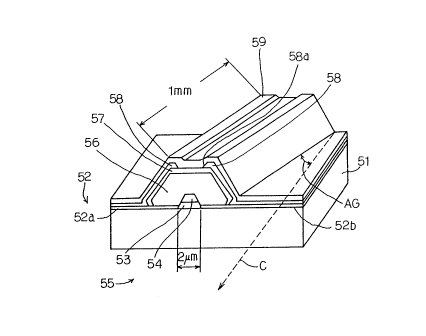
Referring to figure 5 of the~ drawings, asemiconductor laser embodying the present invention is
fabricated on a substrate 51 of n-type indium phosphide
having a major surface 51a with (100) orientation. Arrow C
is indicative of [011 ] direction of the substrate 51.
The semiconductor laser embodying the present
invention comprises an insulating mask 52 of silicon
dioxide covering the major surface of the substrate 51, and
is 1000 angstroms in thickness and 10 microns in width.
The insulating mask 52 is split into two halves 52a and
52b spaced apart from each other by 2 microns, and a center
spacing between the two halves 52a and 52b obliquely
extends at a predetermined angle AG equal to or greater
than 5 degrees with respect to [011 ] direction. The center
spacing exposes a part of the major surface of the
substrate 51. Figure 7 illustrates the layout of the
insulating mask 52, and the two halves 52a and 52b are
hatched for better understanding.
Turning back to figure 6, the semiconductor laser
embodying the present further comprises a buffer layer 53
of n-type indium phosphide grown over the part of the major
13
-
212'`~07 '~
surface and a multiple quantum well 54 with 1.48 micron
wavelength composition grown over the buffer layer 53. The
multiple quantum well 54 serves as an active layer, and
includes six indium gallium arsenide layers each 40
angstroms thick and five indium gallium arsenic phosphide
layers each 130 angstroms thick. The buffer layer 53 and
the multiple quantum well 54 form in combination a mesa
structure 55 having a trapezoid cross section, and the two
halves 52a and 52b of the insulating mask 52 are held in
contact with both sides of a lower portion of the mesa
structure 55.
The semiconductor laser embodying the present
invention further comprises a cladding layer 56 of p-type
indium phosphide 2.5 microns in height and a cap layer 57
of heavily doped p-type indium gallium arsenide 0.3 micron
in thickness. The cladding layer 56 is grown from the mesa
structure 55, and extends on an upper surface of the
insulating mask 52. For this reason, the cladding layer
56 is not directly held in contact with the substrate 51.
The cladding layer 56 has a flat top surface, and the cap
layer 57 also form a flat top surface over the flat top
surface of the cladding layer 56.
The semiconductor laser embodying the present~
14
212~)7~
invention further comprises an insulating layer 58 of
silicon dioxide topographically covering the cap layer 57
so as to create a flat top surface over the flat top
surface of the cladding layer 56. The insulating layer 58
is 2000 angstroms thick, and a slit 58a is formed in the
flat top surface of the insulating layer 58 for exposing
the cap layer 57.
The semiconductor laser embodying the present
invention further comprises an electrode 59 covering the
insulating layer 58 and held in contact with the cap layer
57 through the slit 58a, and the electrode 59 is
implemented by a lamination including a gold film of 4000
angstroms thick and a titanium film of 500 angstroms thick.
Though not shown in figure 6, another electrode is
held in contact with the back surface of the substrate 51.
One of the device facet are coated with a reflecting film,
and the reflecting film is about 95 per cent in
reflectivity. The facets of opposite side are coated with
anti-reflective film, and output light is emitted from the
anti-reflective facet.
The semiconductor laser thus arranged has a length of
the order of 1 millimeter.
In operation, current flows from the electrode 59
through the cap layer 57, the cladding layer 56, the mesa
:~! ' . ;, . ~ .
212~ ~7~
structure 55 and the substrate 51 into the other electrode,
and the semiconductor laser oscillator achieves the light
output equal to or greater than S0 milli-watt.
The multiple quantum well may be replaced with a bulk
active layer with 1.48 micron wavelength composition, and
may be regulated to composition for 1.3 micron wavelength
or composition for 1.55 micron wavelength.
Description is hereinbelow made on a process sequence
for fabricating the semiconductor laser according to the
present invention with reference to figures 8A to 8C taken
along line D-D of figure 7. The process starts with
preparation of the substrate 51, and silicon dioxide is
deposited to 1000 angstroms thick on the major surface of
the substrate 51. The silicon dioxide layer is patterned
into the insulating mask 52 having the dimensions
described in conjunction with the structure of the
semiconductor laser, and the center spacing 52c takes
between the two halves 52a and 52b at 5 degrees with
respect to [011] direction.
N-type indium phosphide, indium gallium arsenide and
indium gallium arsenic phosphide are successively grown on
the exposed center spacing through an metal organic vapor
phase epitaxy. The n-type indium phosphide forms the
16
} .. .
r~ : -
.~ , .
.
..
. ~ . . . . , . . ~ .
212~7~
buffer layer 53, and the six indium gallium arsenide layer
and the five indium gallium arsenic phosphide layers
alternately laminated on one another form in combination
the multiple quantum well 54. Thus, the ~esa structure 55
is formed on the exposed area as shown in figure 8A.
The metal-organic vapor phase epitaxy further grows
the cladding layer 56 of p-type indium phosphide and the
cap layer 57 of heavily doped p-type indium gallium arsenic
phosphide. The cladding layer 56 buries the mesa structure
55, and extends on the insulating mask 52. The cladding
layer 56 reaches 2.5 micron high, and the cap layer is 0.3
micron thick. Even though cap layer 57 projects from the
insulating mask layer by 2.8 microns, the cladding layer 56
and the cap layer 57 keep the top surfaces 56a and 57a flat
as shown in figure 8B, because the mesa structure 55
obliquely extends at 5 degrees with respect to [011]
direction.
Silicon dioxide is deposited to 2000 angstroms thick
over the entire surface of the structure, and the slit 58a
is formed in the passivation film 58 for exposing the flat
top surface 57a. Gold and titanium are deposited to 4000
angstroms thick and 500 angstroms thick over the entire
surface of the passivation film 58, and the gold film and
the titanium film form the electrode 59 through an alloying
17
" ,.
2 ~ 7 4
process. The resultant structure is illustrated in figure
8c.
After the substrate 51 is made thinner by back
surface etching, an electrode (not shown) is formed on the
back surface of the substrate 51. The semiconductor laser
are separated from one another through a cleavage step in
such a manner as to be 1 millimeter in length.
As will be appreciated from the foregoing
description, the injected current flows through the
cladding layer 56 to the mesa structure 55 without leakage
current, and achieves the large light output. Moreover,
the process sequence according to the present invention
successively grows the buffer layer 53, the multiple
quantum well 54, the cladding layer 56 and the cap layer 57
without partially removing stage for the insulating mask
52. Therefore, only one sequence of MOVPE process is
required, while the prior art process require two sequence
of MOVPE. In fact, the selective MOVPE is completed within
half time period of the prior art process. Finally, the
process sequence according to the present invention is good
in reproducibility.
Second Embodiment
Referring to figure 9 of the drawings, a
18
... . ,, . ., ~ .- - ~ - :: -
. :: . . . .
.;A; . ~ ~
2l2~n7~
semiconductor optical amplifier or a semiconductor LD
amplifier is fabricated on a substrate 61 of n-type indium
phosphide. The n-type indium phosphide has a major surface
61a with (100) orientation, and arrow C'~ is indicative of
[011] directlon.
The semiconductor optical amplifier is fabricated
through the following process sequence. An insulating mask
62 is provided on the major surface of the substrate 61,
and the insulating mask 62 is split into two portions 62a
and 62b spaced apart from one another by 0.7 micron as
shown in figure 10. The portions 62a and 62b are 700
angstroms in thickness and 10 microns in width. The center
spacing 62c obliquely extends at 10 degrees with respect
to [011] direction, and exposes a part of the major surface
61a of the substrate 61.
A buffer layer 63 of n-type indium phosphide and an
active layer 64 of indium gallium arsenic phosphide are
grown on the exposed center spacing 61a through a metal
organic vapor phase epitaxy as shown in figure 11. The
indium gallium arsenic phosphide is regulated to a
predetermined composition for 1.3 micron wavelength, and is
3000 angstroms thick. The active layer 64 is 5000
angstroms wide at the intermediate point of the thickness,
and the buffer layer 63 and the active layer 64 form in
!:`' .', . :. - .-
'' ,: :, ;
~':- . .
~, , : :
~". . ,
;': ' . :-
'' `:, ` : : . . : :
212~74
combination a mesa structure 65. The portions 62a and 62b
are held in contact with the lower portion of the buffer
layer 63.
As similar to the first embodiment, a cladding layer
66 of p-type indium phosphide and a cap layer 67 of heavily
doped p-type indium gallium arsenide are continuously grown
over the mesa structure 65 through the metal organic vapor
phase epitaxy (see figure 9 again). The cladding layer 66
extends on the insulating mask 62, and is not directly
contact with the ma]or surface 61a.
Although the cladding layer 66 is 1.5 micron high and
the cap layer 67 is 0.3 micron thick, the top surfaces
thereof are flat, because angle AG' is not less than 5
degrees. ;
Silicon dioxide is topographically deposited to 2000
angstroms over the entire surface of the structure for
forming an insulating layer 68, and a slit 68a is formed in
the top surface of the passivation film 68 for exposing the
flat top surface of the cap layer 67. Gold and titanium
are deposited to 4000 angstroms thick and 500 angstroms
thick over the entire surface of the structure, and the
gold film and the titanium film are formed into an
electrode 69 through an alloying technique. ~
2~2~7~
The back surface of the substrate 61 is grinded, and,
thereafter, an electrode is provided on the grinded back
surface. The semiconductor light amplifiers are separated
through a cleavage, and the device length is regulated to
500 microns.
In operation, current was in~ected through the
cladding layer into the active layer 64, and the
semiconductor optical amplifier achieved more than 25 dB
for an incident light with 1.31 micron wavelength under 200
milliamperes.
The active layer 64 may be formed of indium gallium
arsenic phosphide with 1.55 micron wavelength composition
for incident light with 1.55 micron wavelength.
As will be appreciated from the foregoing
description, the semiconductor light amplifier achieves a
large gain, because the current flows into the active layer
without leakage current into the substrate 61, and the
process sequence i~ simpler than the prior art process.
The process sequence according to the present invention is
good in reproducibility.
Third Embodiment
Referring to figure 12 of the drawings, a
electroabsorption optical modulator embodying the present
invention is fabricated on a substrate 71 of n-type indium
.. ~ . . . ....
. . . ~ ~ . . ..
~2~107~
phosphide. The indium phosphide crystal has (100) surface
serving as a major surface of the substrate 71.
The structure of the electroabsorption optical
modulator will be understood through description on a
process sequence with concurrent reference to figures 13A
to 13C.
First, an insulating mask 72 is provided on the
major surface, and is split into two portions 72a and 72b
spaced apart from one another by a 2 micron wide center
spacing. The two portions 72a and 72b are 3000 angstroms
in thick and 15 microns wide. The center spacing obliquely
extends at 10 degrees with respect to [011] direction
indicated by arrow C".
Using a metal organic vapor phase epitaxy, a buffer
layer 73 of n-type indium phosphide and an optical
absorbing layer 74 are successively grown on the exposed
area of the major surface of the substrate 71. The optical
absorbing layer 74 is 2500 angstroms thick, and the indium
gallium arsenic phosphide is regulated to the 1.45 micron
wavelength composition. The buffer layer 73 and the
optical absorbing layer 74 form a mesa structure 75.
The metal organic vapor phase epitaxy further grows a
cladding layer 76 of p-type indium phosphide and a cap
. . , -:
~,
,:, , . :
'b
2~2r~r37~
layer 77 of heavily doped p-type indium gallium arsenide
over the mesa structure 75, and the insulating mask 72
prevents the cladding layer 76 and the substrate 71 from
direct contact. The cladding layer 76 is~1.5 micron high,
and the cap layer 77 is 0.3 micron thick. However, the
cladding layer 76 and the cap layer 77 keep the top
surfaces thereof flat, because the mesa structure 75 is
grown on the exposed center spacing declining at more than
5 degrees with respect to [011] direction.
While the buffer layer 73, the optical absorbing
layer 74, the cladding layer 76 and the cap layer 77 are
growing through the metal organic vapor phase epitaxy, an
n-type indium phosphide layer 73a, an indium gallium
arsenic phosphide layer 74a, a p-type indium phosphide
layer and a heavily doped p-type indium gallium arsenide
layer are simultaneously grown on the major surface outside
of the insulating mask 72 as shown in figure 13A.
These layers 76a to 77a are etched away by at least 1
micron thick as shown in figure 13B. Silicon dioxide is
deposited over the entire surface of the structure to 2000
angstroms thick so as to form a passivation layer 78, and
the passivation layer 78 is coated with polyimide 79 as
shown in figure 13C.
The polyimide layer 79 and the passivation layer 78
23
~ -.,... :: - . .. .
~ ~ ,, , . ~ ! .
~'" ~ ' ' ' ,' ,. ..
2~2~7~
are partially removed to expose the flat top surface of the
cap layer 77, and gold and titanium are deposited to 4000
angstroms and 500 angstroms over the entire surface of the
structure. The gold film, the titanium film and the
polyimide layer 79 are patterned as shown in figure 12.
The gold film and the titanium film are formed into
an electrode 80 through an alloying step. The substrate is
made thinner by back surface etching. An electrode (not
shown) is formed on the back surface, and the semiconductor
optical modulator with a device length of 300 microns is
separated through a cleavage. An anti-reflective film (not
shown) covers the device facets.
The electroabsorption optical modulator embodying the
present invention achieved the extinction ratio at 20 dB,
the optical loss at 3 dB and the modulation band width of 5
GHz. When the electroabsorption optical modulator was
coupled to an optical fiber, the coupling loss was 2.5 dB.
In this instance, the insulating mask 72 was 3000
angstroms thick. However, if the insulating mask 72 of
silicon dioxide is not less than 2000 angstroms, the
modulation bandwidth of 2.4 GHz is achievable.
The optical absorbing layer 74 may be replaced with a
multiple quantum well structure implemented by a~
24
:~; . ~ ., . - .
;,. ~ . -. . . . : ~ - ,
.: , ~
. - . . . . .. .
.
. . .
2~2~7~
alternately laminated six indium gallium arsenide layers
each 30 angstroms thick and five indium gallium arsenic
phosphide layers with 1.3 micron wavelength composition
each 130 angstroms thick. The structure is of oscillating
wavelength of 1.45 microns composition.
As will be understood from the foregoing description,
the insulating mask layer 72 prevents the substrate 71 from
leakage current from the cladding layer 76, and the thick
insulating mask 72 decreases the parasitic capacitance not
greater than 1 pF. As a result, the electroabsorption
optical modulator according to the present invention
achieves the good performances.
Moreover, the process sequence according to the
present invention grows the buffer layer 73 to the cap
layer 77 through a single metal organic vapor phase
epitaxy, and, for this reason, is simpler than the prior
art process sequence without sacrifice of reproducibility.
Although particular embodiments of the present
invention have been shown and described, it will be obvious
to those skilled in the art that various changes and
modifications may be made without departing from the spirit
and scope of the present invention. The selectively
growing technology is not limited to the metal organic
vapor phase epitaxy, and the compound semiconductor
- - . . .- .- - . - . . . . ... j., - .
2~2~07~
materials used for the semiconductor optical device may be
in a different system. The semiconductor optical devices
according to the present invention may be fabricated on p-
type semiconductor substrates by changing the dopant
impurities of the compound semiconductor layers to the
opposite type to those of the semiconductor optical devices
described hereinbefore.
The insulating mask layers, the insulating layers and
the passivation layer may be formed of PSG or SiON.
26
".~
,. . ~ ~ ' ' :
.~ : , ,.