Note: Descriptions are shown in the official language in which they were submitted.
2129080
BACKGROUND OF Th~ lN v~NllON
--This invention relates to FDDI networks, and more
particularly to a low cost, fault tolerant FDDI wiring Hub.
FDDI (Fiber Distributed Data Interface) is a high speed
data interface designed with Fiber optics in mind, although
of course the interface can be used with other transmission
media, such as shielded twisted pair lines.
Traditional FDDI networks use two methods to
interconnect stations: point to point connection of dual-
attached stations in a ring topology; or connection ofsingle-attached stations to an FDDI concentrator in a star
topology.
Point to point connection retains the fault tolerance
of FDDI but is difficult to maintain. The ring topology is
essential in the networks ability to recover from a fault.
Removal or addition of a station involves re-wiring a
portion of the network to maintain the proper topology. -
During this time, the network is unable to recover from a
fault. --
Intelligent FDDI concentrators connect single-attached
stations in a star configuration. They are relatively
expensive and can be a single point of failure in an FDDI
network since each station only has one connection to the
ring rather than two. Replacement of a faulty concentrator
results in a disruption of service for all stations
connected to that concentrator.
- 2129080
Neither of these interconnect methods are adequate for
backplane applications where reliability and ease of re-
configuration are important. '
SUMMARY OF T~ lNv~NllON
An object of the invention is to alleviate the afore-
mentioned problems by providing the configuration
flexibility of a star-wired network while maint~;n;ng the
fault tolerance of dual-attached stations on the FDDI ring.
Accordingly the present invention provides a wiring hub
for interconnecting a plurality of switching units,
comprising: a plurality of interface modules for connection
to respective external packet switching units in a dual-
attached connection; transmission paths interconnecting said
interface modules in a manner consistent with FDDI ring
topology to permit a dual-attached FDDI ring to be
established through said external packet switching units;
and said interface modules including a switching element
operable to bypass each switching unit or insert it on the
ring in a dual-attached connection, said switching element
automatically switching the interface module to its bypass
state when a packet switching unit is disconnected from the
wiring hub.
In a preferred embodiment, the packet switching units,
are high speed frame relay switches.
When a station-is disconnected from its interface
module, the module automatically switches to the bypass
2129080
state restoring the dual FDDI ring. If an interface module
fails, the FDDI ring will wrap around it and maintain
operation of the remaining stations. The interface-module
may be replaced without any further disruption of service.
Low cost is achieved by preferably using shielded
twisted pair cable rather than fiber optics.
Power for each interface module comes from the station
to which it i8 connected. The lack of a centralized power
supply means that a failure will only affect a single
station, not the entire wiring hub.
Stations may be added or removed from the network by
simply plugging or unplugging them from the hub. When a
station is connected to the hub and inserted on the ring, it
is a full dual-attached station with all the advantages of
point to point connection with its neighbors. When a
station is connected to the hub, and not inserted on the
ring, it can perform a link confidence test on its
connection to the hub while the re~;n~er of the stations
remain connected in a full dual-ring. The station therefore
has the same advantages as being connected to an intelligent
concentrator but with the added improvement of being dual
attached.
This FDDI wiring hub may be used in twisted pair based
FDDI networks where low cost and fault tolerance are primary
concerns.
BRIEF DESCRIPTION OF 1~ DRAWINGS
2129080
The invention will now be described in more detail, by
way of example only, with reference to the accompanying
drawings, in which:- -
Figure 1 is an example of one application of a wiring5 hub in accordance with the invention;
Figure 2 is an exploded view of a wiring hub asæembly
in accordance with the invention;
Figure 3 shows an arrangement for matching the printed
circuit board (PCB) trace impedance to the STP (Shielded
Iwisted Pair) cable of the FDDI ring.
Figure 4 shows the interface modules connected in dual-
attached ring topology;
Figure 5 shows an STP module for connection to an FDDI
ring;
Figure 6 shows a cascade module for use with a shielded
twisted pair connection; and
Figure 7 shows a cascade module for use with a fiber
optic connection.
DESCRIPTION OF THE PREFERRED EMBODIMENTS
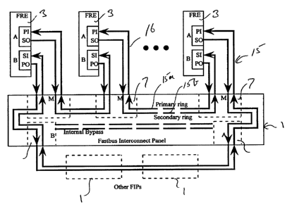
Figure 1 shows an application of the wiring hub or FIP
(FASTbus Interconnect panel) 1 in accordance with the
invention. As shown in Figure 1, the wiring hub 1 is
connected to two FRE (Frame relay Engine) cards 3 in
Newbridge Networks Corporation 3600 MainStreet~ muliplexers
2, which are connected via T1 modules to 8230 MainStreet~
2129080
bridges 6 that are connected to respective Ethernet~ LANæ
5. The FRE cards 3 provide a high speed frame relay packet
switching function.
The wiring hub 1 forms part of the Newbridge FASTbus~,
which consists of high-capacity frame relay switches
implemented in the 3600/3645 MainStreet~ product, linked by
a high-bandwidth bus operating under the Newbridge 4602
MainStreet~ Network Management system. This allows users
to add Frame Relay Engine (FRE) cards to the network map,
configure them, connect them on the map via a 36120
MainStreet~ node, and route frame relay paths (FRPs) over
them from a single network node using the 4602 MainStreet~
system.
In the network shown in Figure 1, wiring hub 1 provides
the center of a frame relay network. User data is assembled
into frame relay packets on the 8230 MainStreet~ Ethernet
Bridges 6. The packets are switched in 3600 MainStreet~ or
3645 MainStreet~ nodes two by FRE cards 3, such that they
travel to other FRE cards 3 via the wiring hub 1, and are
eventually disassembled into user data on another 8230
MainStreet~ bridge 6.
The wiring hub 1, which is shown in more detail Figure
2, is intended to be a low cost product for interconnecting
Frame Relay Engine (FRE) cards on an FDDI ring. It provides
the interconnection at the Physical Medium Dependent (PMD)
layer as opposed to the Physical (PHY) layer of FDDI. As
such, it is strictly a wiring hub, as opposed to a true FDDI
Concentrator.
2I29080
The wiring hub 1 consists of a 19 n rack mount chassis 1
with twelve plug-in interface modules 7, i.e. one for each
port, and with the FRE cards 3 forms a dual FDDI ring 15
consisting of primary ring 15a and sec~n~ry ring 15b.
There are thus 12 M ports for connection to FRE cards, an A
port, a B port and a spare. The A and B ports are used to
cascade wiring hubs into larger systems as be be explained
in more detail below. An unconnected spare port is
available to store an extra module.
The interface modules 7 are connected to the FRE cards
..3 by ~hielded twisted pair cable 17 (STP), which forms part
of a dual-attached FDDI ring through the FRE cards 3.
The metal chassis 11 provides shielding for both EMI
and ESD. The chassis 11 is well connected to ground. The
rear of the chassis 11 provides two grounding points which
may be used if the rack in which the hub is installed is not
grounded. The module faceplates are screwed to the main
chassis to provide mechanical support and to ensure that the
faceplates and therefore the cable shields are well
grounded.
The chassis contains a bac~plane 12, which provides the
interconnection of the interface modules 7, and a separate
board-13 containing the faceplate LEDs 14, which indicate
the status of the ports of the wiring hub 1. A ribbon cable
9 connects the LED board 13 to the backplane 12.
The function of the backplane 12 is to connect primary
and secondary ring data of adjacent interface modules 7 at a
data rate of 125 Mbps and to pass the LED signals from the
21290~0
interface modules 7 through to the LED board 13. This is
done over microstrip transmission lines 18.
In view of the high data rate, track impedance is
important. Ideally, the trace impedance should match the
STP (Shielded Twisted Pair) cable impedance of lOOQ. When
- considering ~alanced differential signals, the configuration
shown in Figure 3 properly matches the lOOQ cable to looQ
(differential) traces. The track impedance (with respect to
the ground plane~ is as close as possible to 50Q. The
physical ~;men~ions required to realize this impedance are
calculated on the basis of the following formula for a
microstrip transmission line:
87 5.98h
zo = ln
~Er + 1.41 0.8W + t
Where: Zo = impedance of line (~)
Er = dielectric constant
h = distance between signal line and
reference
plane (in)
W = width on line (in)
t = thickness of line (in)
Using a no~; n~l O . 010 in. dielectric thickness, a trace
of width 0.017 in. will result in a trace impedance of
49.9Q. This is well within the impedance tolerance which.
most PCB shops will guarantee.
The routing of the signals is also important and should
be as short as possible with signal pairs routed adjacent
-- 7
212~080
and parallel to each other. Shielding to reduce crosstalk
is provided by routing a GND (ground) trace between adjacent
pairs where necessary. This GND trace will be connected to
the GND plane about every 1 n to ensure an adequate shield.
S As shown in Figure 4, the FREs 3 are connected to the
wiring hub by shielded twisted pair cable (STP) 16. Three
interface modules 7 are shown connected to respective FRE
cards 3.
The interface modules 7 actually consist of one or more
different types of module, namely an STP Module for
connection to the FRE cards 3 over the shielded twisted
pair, a bypass module for bypassing unused module positions,
an STP cascade module for cascading hubs together in high
capacity systems, and Cascade Fiber Module for use when the
distance between cascaded hubs is too great for twisted pair
cable.
Figure 5 shows an STP module in more detail. The cable
from the FRE card 3 connects to a male DB-15 connector 16
(Figure 3) on the interface module. When referring to signal
names, all signals are named with respect to the FRE card to
which they connect. For example, Primary In refers to the
signals which drive the A-port receiver on the FRE card. On
the interface module, the Primary In signals are output~ on
the DB-15 that connects to the FRE card and inputs on the
backplane connector.
Each STP module consists of relays 30 that are
connected to the FRE card 3 via buffers 32 and transformers
19. The STP modules are energized when the FRE card 3
-- 8
2I2908o
asserts its in~ert signal. Power to energize the relays 17
is provided by the F~E card 3 over the shielded twiæted pair
17. Therefore, when no power is received (as when nothing
is connected) the relays remain in a bypassed state. When
the relays 31 are energized, an insert LED on the faceplate
is driven.
An open collector activity signal from the FRE card 3
is passed through to the backplane to drive the
corresponding faceplate LED.
Transmit and receive data are transformer coupled upon
entering the module from the FRE card 3. This allows the
module to terminate the common-mode cable detect signal
appropriately for the FRE's A and B ports. The module must
source cable detect current (from ~12V) on the Primary In
pair and sink the cable detect current (to GND) on the
Secondary Out pair. This mimics M-port cable detect. The
Primary Out and Secondary In pairs mimic S-port cable detect
by shunting the cable detect current from Primary Out to
Secondary In. Using the M- and S-port cable detect methods
in this way ensures that all four data pairs are correctly
connected from the F~E card to the hub.
Transmit and receive data are connected directly to the
hub backplane.
The bypass module (not shown~ is installed in unused
module positions to effectively bypass them. It simply
connects the Primary In to Primary Out s~ignals and the
Secondary In and Secondary Out signals to complete the dual
rings. This card contains only the bac~plane connector, an
2129080
option resistor for the insert LED and a module faceplate.
Bypass modules must be installed in all unused module
positions (including cascade ports) to complete the~dual
ring.
S Cascade STP modules 20 (Figure 6) are installed in the
A and B portæ of the Hub to link fieveral hubs together using
shielded twisted pair cable. This module uses a female DB-
15 connector rather than the male DB-15 used on the STP
modules to prevent improper cabling. The STP modules consist
of buffers 21 and transformers 22.
Signal buffering is performed by this module in the
same manner as the STP module. This ensures that the
hub to hub cable length can be met.
No relays are present on this module. If nothing is to
be connected to the cascade port, then a bypass module is
used in place of a cascade module. Depending upon which
port this module is installed in, either the Primary In /
Secondary Out or Secondary In/Primary Out set of signals is
brought out to the connector. The modules themselves are
identical, however, the backplane brings out the appropriate
signals to the A and B cascade ports.
Separate cable detect between hubs is implemented.
Extra wires in the cascade cables are used for this purpose.
When a cascade cable is properly connected, the insert LED
2S on the hub faceplate will be illuminated. The cable detect
pair simply pulls the backplane LED signal low. To keep the
hub grounds isolated, each hub uses a separate pair for
cable detect.
-- 10 --
2129080
If the distance between hubs is too great for twisted
pair cable, fiber optics may be used in its place. The
Cascade Fiber module 23 ~Figure 7) is similar in function to
the Cascade STP 20 module but replaces the DB-15 with a pair
of optical ST connectors 24.
Receive signal detect from the optical module is used
to illuminate the cascade LED on the faceplate when this
module is used. This indicates that a valid optical signal
is being received and is indicative of proper cabling.
The described wiring hub provides a low cost, reliable,
serviceable alternative to FDDI concentrators in
applications where re~lln~ncy is not a ~trict requirement.
Given the fault recovery mech~n;sr employed by FDDI Station
Management (SMT) software on the FRE cards, hub reliability
becomes somewhat relaxed in the sense that the failure of
virtually any hub component will not bring down the entire
FDDI ring. The Station Management software can maintain an
operational ring by wrapping the ring on each side of the
failed equipment. The hub allows the failed components to
be replaced while the ring rem~;n~ operational.
In a single hub system, no failure of the wiring hub
will cause a Class 1 system failure. This class of failure
is defined as one in which 50~ of the system's subscrib.ers
are down. In cascaded systems, loss of both cascade modules
2s would result in isolating the group of FRE cards connected
to that hub.
2129080
The described wiring hub thus provides an effective
low-cost solution for FFDI networks. Some highlights of the
solution are: -
Automatically bypasses FRE cards if cables are5 removed or broken.
Uses relays to achieve high reliability and low
cost on each module.
Requires no power supply - power is sourced from
each FRE card.
Front panel LEDs give individual card insert and
activity status.
Provides STP (Shielded twisted pair) or Fiber
Optic interfaces for cascading hubs.