Note: Descriptions are shown in the official language in which they were submitted.
WO 93/~649~ 2 ~ 2 9 1 2 ~ PCT/US93/01322
HIGH DENSITY ELECTRONIC CIRCUIT MODULES .:
Backqround of the Invention
The development of new portable electronic products, ~ :
such as the laptop computer, is currently o~ great
worldwide interest. Miniaturization of the various
component systems (memories, displays, and so forth) for
such products requires that the necessary circuits be
packed in as small a volume as possible. Packing circuits
into a small volume also reduces parasitic capacitance and
lo improves signal propagation time between circuits. One
approach to this requirement is to increase the scale of
integration in order to obtain all of the required
functions from a ~ircuit made from a single wafer.
Unfortunately, efforts to create ~ull-wafer circuitry have
encountered unacceptable yield losses owing to the large
circuit size. In the specific area of active matrix ~
displays, a similar problem results in attempting the ....
scale-up of the display size to and beyond the 256K pixel
level.
Active matrix (AM) displays generally consist of
flat-panels consisting of liquid crystals or
electroluminescent materials which are switched "on" and ~:~
"off" by.electric fields emanating from pixel electrodes
charged by thin-film transistors (TFT's) co-located with ~.
each liquid orystal or ~lectroluminescent pixel area.
These~AM-displays are expected to supplant cathode ray
tube`(CRT) technology and provide a more highly defined
television picture or data display. The primary advantage
of the active matrix approach, using TFT's, is the :
elimination of-cross-talk between pixel~, and the
excellent grey scale that can be attained with TFT~
: compatible liquid crystal displays ~LCD's~.
Flat panel displays employing LCD's generally include .
five different layers: a white light source layer, a -~
-
212~2~
W~93/l~gl ` PCT/US93/01322'~
2--
first polarizing filter layer that is mounted on one side
of a circuit panel on which the TFT's are arrayed to form
pixels, a filter plate layer containing at least three
primary colors arranged into pixels, and finally a second
polarizing filter layer. A volume ~etween the circuit
panel and the filter plate is filled with a liquid crystal
material, This material rotates the polarization of light
passing through it when an appropriate electric field is
applied across it. Thus, when a particular pixel
electrode of the display is charged up by an associ~ated
TFT, the liquid crystal material rotates polarized light
being transmitted through the material so that it will
pass through the second polarizing filter and be seen by
the viewer.
The pri~ary approach to TFT formation over the large
areas required for flat panel displays has involved the ~ ;
use of films of amorphous silicon which has previously
been developed for large-area photovoltaic devices.
Although the TFT approach has proven to be feasible, the
use of a~orphous silicon compromises certain aspects of
the panel performance. For example, amorphous silicon
TFT's lack the ~requency response needed for large area
displays due to the low electron mobility inherent in
amorphous material. Thus, the use of amorphous silicon
limits display speed, and is also unsuitable for the fast
logic needed to drive the display.
owing to the limitations of amorphous silicon, other
alternative materials are being considered, such as,
polycrystalline silicon, or laser recrystallized silicon~
30 Thin films, less than about 0.4 microns, of these -~;~
materials are usually formed on glass which generally
restricts further circuit processing to low temperatures.
The formation of large activematrix displays is
hampered by the una~ailability of large-area single
crystal Si material~ Thus the conventional approach is to
v~ 2129123 ` ~
WO93/1~91 PCT/US93/01322
use thin-film amorphous (A Si) or polycrystalline Si
(poly-Si) wafers. The required number of thin-film
transistors ~TFT's~, combined with the large number of
driver circui~s ~nd the thin-film material defects
5 inherent in A-Si or poly-Si, leads to unacceptable yield
and quality problems when the entir~ display is to be -~
fabricated as a u~it~
A need exists, therefore, for a relatively
inexpensive way to reliably form hybrid high density
electronic circuits, including active matrices, me~ories,
and other devices, in a modular approach that permits
small high-guality parts or circuits to be assembled into
complete large-area high-quality complex devices.
Summary of ~he Inv~nti~n
15The prlesent invention co~prises a method, and
resulting a]pparatus, for fabricating complex hybrid multi-
function circuitry on or in a common module body, such as
a su~trate or superstrate, by using ~ilicon thin film
transfer proces~es to remove areas or tiles of circuits,
formed in Si thin-films, and trans~erring, locating and
adhering the removed tiles to a common module body. The
removal of areas or tiles is hereinafter referred to,
generally, as "dicing." The process of transferring,
locating and adhering is generally referred to as
2~ ~Itiling~
~ The films may be formed of A-Si, poly-Si, or x-Si
depending upon~the desired circuit parameters. ~lements
of one circuit are then interconnected to elements of
another`circuit by conventional photolithographically
30 patterned thin film metallization techniques. Direct ~ -
laser writing or erasing may be used for repair or
modification of interconnects.
The transfer may be accomplished in either of two
ways - single transfer or double transfer. In the single
.
2~2gl~
WO93/1~91 PCT/~S93/01322
--4--
transfer process, the desired Si circuitry is formed on a
thin film Si substrate; the Si circuits are diced, i.e.,
divided into dice or tiles containing one or more
circuits; ~he dice or tiles are then tiled, i.e.,
sequentially registered onto a common module ~ody and
sequentially adhered to the module body. After all the
dice or tiles are adhered to the module body, all the Si
sS~kstrates are removed in one process and the circuits
interconnected. Alternately, the Si substrates may be
sequsentially removed if more precise alignment is
required .
In the double transfer process, the circuits are
transferred to an intermediary transfer or carrier body
and then the substrates are removed. Dicing may occur
before or aXter the first transferral. The thin film
circuitry is supported by the transfer body until transfer
to the com~Son module body is appropriate. The circuitry
is then tiled, i.e., sequentially transferred, regi~tered
and adhered to the common module body. If the transfer
body i5 sufficiently thin, the transfer body may be left
on the circuitry. If not, it i8 removed and circuit
interconnections made, as required.
In a preferred embodiment, the com~Son module forms an
active matrix tAM) LCD panel fabricated in accordance with
the in~ention. The circuit panel for the AMLCD is formed
~y transferring to a common module ~ubstrate or
superstrate, multiple x-Si and/or A-si or poly-Si thin
film tiles upon which circuits ~Say have been for~sed, and
wherein each tile is obtained as a~ unit from one or more
wafers. During transfer, the tiles are registered with
respect to one another. Circuits are then interconnected
as necessary. Registration is accomplished by well-known
X-Y micropositioning equipment. Adherence and planarity
are achieved using optically transparent adhesives which
fill in voids left in forming circuitry. Trimming of
'.
f wo 93~1~91 ` 2 1 2 9 ~ 2 3 PCT/US93/01322
--5-- ::
substrate edges may be required to obtain precise circuit
dimensions needed for proper alignment on the module body.
Other preferred embodiments of the present invention
relate to the ~ormation of three-dimensional circuits and
devices. Siynificantly, these three dimensional circuits
and devices provide for high density circuitry in small
areas. As such, three-dimensional (3-D) circuits and
devi~s can be used to fabricate high density electronic
cir ~ry including stacked memories, multi-functional ;
par~_el processing circuits, high density low-power CMOS
static ~AMs, peripheral drive circuitry for display panels
and a plurality of high-speed low-power CMOS devices.
In accordance with the present invention, a prefexred
fabrication process comprises single and double transfer
of silicon films and back~ide processing of said ~ilms for
providing various 3-D circuits and devices. In one
preferred embodiment, a 3-D double gate MOSFET device can
be fabricated. First, a standard MOSFET having drain,
source and gate regions is formed in a silicon layer of an
20 SOI structure by any suita~le technique. Next, the MOSFET ;
is single transferred to a superstrate for backside
process~ng. A region of the insulating layer is removed
to expose a back~ide region of the silicon layer. A
second gate is then formed adjacent the backside region of
the silicon layer opposite the first gate. A conductive
contact is at~ached to the second gate, thereby providing
a 3-D double-gate MOSFET.
In~another embodiment of the present invention~-a 3-D
double gate MOSFET inverter is fabricated s~ch that its n-
channel ~OSFET and itB p-channel MOSFET share the same -;
body with their respective channels disp~sed on opposite
sides of the shared body. In fabricatin:~- this inverter, a
silicon layer is formed over an insulat1~ layer on a
substrate. After the silicon is patterned into an island,
a series of doping steps are performed on the silicon to
212~12~
W093/1~91 PCT/US93/01322
--6--
produce a first MoSFET having a first drain, a first
source and channel region (which is a portion of the
shared body region3. The first drain, first ~ource and
channel regions are disposed along a first axis in a plane
extending through the ~ilicon. Another series of doping
steps are subsequently performed on the silicon to produce
a second MOSFET having a second drain, a second source and
a channel region which are disposed along a ~econd axis
extending perpendicular to the first axis. A first gate
iS then formed on one side of the plane of the ~ilicon,
and contact~ are attached to the first source, first
drain, first gate, second source and second drain. The
silicon is bonded to a superstrate and the substrate is ~-
removed for backside processing. Accordingly, a region of
the insulati.ng layer is removed to exposed a backside
region of the silicon island and a second gate is formed.
The second gate is positioned on the opposite side of the --
plane of the silicon island as the first gate over the
channel region. A contact i5 then attached to the second ~ ~`
gate and the two gates can then be electrically connected.
In another embodiment, another 3-D double gate MOSFET
inverter is formed of a pair of vertically stacked
MOSFETs. T~e fabrication sequence involves forming a
first MOSFET device in a first silicon layer over a first
substrate, and a second MOSFET device in a second silicon
layer over a second substrate. The first MOSFET device is
transferred to a superstrate, and the second MOS~ET device
is transferred to a optically trans~issive substrate.
Next, the first silicon layer i5 stacked onto the second
silicon layer such that the two MOSFET devices are
vertically aligned. The MOSFETs are then electrically
interconnected to provide an 3-D inverter circuit.
In yet another embodiment, a vertical bipolar
transistor is fabricated in accordance with the principles
212~3 ~ `
Wo93/t~sl PCT/~S93/01322
-7-
of the inYention. The fabrication process begins with
providing a silicon layer over an insulating layer on a
substrate. Nex~, a series o~ doping steps are performed
to produce a collector region, an emitter region a~d a
S base region. Conductive contacts are then formed for the
collector, emitter and base. The structure can be 6ingle
transferred to a superstrate for backside proces~ing. To
that end, a region of the insulating layer i~ removed to
expose a backside region of the silicon layer. A metal
layer is applied over the exposed backside of the silicon
and sintered.
Integrated circuits fabricated and other materials
can also be stacked into 3D circuit modules according to
the invention. ~he circuits can be fabricated and I~
II-YI, or }II-V compounds or in diamond thin film~. In
addition, 3D circuit modules may comprise stacked layers
or differring materials.
According to preferred embodiments of the invention, ; -~
various circuit layers in 3D ~odules may be
interconnected. The circult layerfi may be interconnected
by conductive material, or by contactless coupling. In a
3D circuit module, the circuit layers adhered to each
other my interleaved thin ~il~ epoxy layers.
Interconnects form a patterned layers to form vias and
then depositing a thin film ~etallization layer into the
__ vias. In an alternate preferred embodiment, the circuit
layers are interconnected by optical couplers. In yet
another pre~erred embodiment, the circuit layers are
coupled by compassitive or inductive coupling elements.
Stacked 3D circuit module~ according the subject
in~ention comprise thermally conductive layers interleaved
into the stacked circuit layers to enhance heat transfer
to an external heat sink the thermally conductive layers
are fabricated as thin film layers. The thermally
conductive layers may comprise of thin film diamond,
212~2~
WO93/16491 - PCT/US93/01322
-8-
silicon carbide, aluminum nitride, alumina, zurconium,
ceramic material or bralium oxide.
Brief Description of the Drawin~s
Fig. l is a perspective ~iew of a high density
circuit module in the form of an active matrix liguid
crystal display (AMLCD).
Fig. 2A is a schematic illustrating how two six inch
wafers can be used to form tiles for a 4 X 8 inch AMLCD.
Fig. 2B shows the tiles of Fig. 2A applied to a glass
substrate for forming an AMLCD.
Fig. 3 is a circuit diagram illustrating the driver
system for t:he AMLCD of Fig. l.
Figs. ~L~-4L is a preferred process flow ~equence
illustrating the fabrication of the ~ portion of the
circuit panel for the AMLCD of Fig. l.
Figs. ~jA and sB are cross-sectional schematic process
views of a portion of the AMLCD.
Fig. 6 illustrates in a perspective view a preferred
embodiment of a system used for recry~tall~zation. ;
~0 Figs. 7A-7D is a process flow seguence illustrating
transfer and bonding of a silicon an oxide (SOI) structure
to a glass superstrate and removal of the substrate.
Figs. 8A and 8B is a process flow sequence
illustrating an alternative transfer process in which a
GeSi alloy is used as an intermediate etch step layer.
Figs~ 9A and 9B is a process flow sequence
illustrating another thin f~lm tile isolate and transfer ;~
process used to form a pressure sensor or an array of such
sensors.
Fig. l0A-and lOB illustrate an alternate process to
the procéss of Figs. 9A and 9B.
Figs. llA-llD is a process flow sequence illustrating
circuit transfer steps employed in the ormation of a
khree-dimensional circuit.
'~. ' ~ '
;~ ~' " -' '
- -
2~29123 . -- .
WO93/1~91 PCT/US93/01322
_9_
Figs. 12A and 12~ are graphs illustrating the drive
current and transconductance of a MOSFET circuit
surrounded by an adhesive and positioned on a glass
substra~e and a MOSFET circuit surrounded by air and
positioned on a glass substrate respectively.
Figs. 13A and 13B is a process flow 6equence
illustrating t~e formation of electrical interconnections
between layered devices.
Fig. 14 illustrates a 6hielding layer positioned in a
layered structure for minimizing undesirable electrical
interference between layered devices.
Figs. 15A-15G is a process flow sequence illustrating
the fa~rication of a 3 D double gate MOSFET device.
Figs. 16A-16J is a process flow sequence illustrating
the fabrication of a 3-D double gate inverter.
Figs. 17A-17D is a process flow sequence illustrating
the fabrication of a 3-D stacked inverter.
Figs. 18A-18~ is a process flow sequence illustrating
the fabrication o~ a vertical bipolar transistor.
Figs~ l9A-19D illustrate the ~abrication of a III-V
circuit array.
Figs. 20 is a plan view of an XY addressable LED
array mounted or stacked on a silicon substrate with an
associated silicon electronic circuitry.
Fig. 21 is a schematic side view of an infrared to
visible light converter embodiment of the invention.
~ Fig~-22 1s a side view o$ a pixel of a~tri-color X-Y
addressable LED array. ~ - -
Fig. 23 is a plan view of the array of Fig. 22. -
' 30 Figs. 24A-24C illustrate preferred embodiments of
- interconnecting 3D circuit stacks. - ~
Figs. 25A-25C illustrate a preferrec ~mbodiment of a
thermally managed 3D stack.
w~a~ 2 3 PCT/US93~0132~
--10--
Details De~8~i~i~ g~he Invention
X. Tiled Active Matrix Liquid.Crystal Display
A preferred embodiment of the in~ention for
fabricating complex hybrid multi-function circuitry on
5 common module substrates is illustrated in the context of
an AMLCD, as shown in Fig. 1. The basic components of the
AMLCD comprise a light source 10~ such as a flat
fluorescent or incandescent white lamp, or an
electroluminescent lamp ha~ing white, or red, blue and ~ :
10 green phosphors, a first polarizing filter 12, a circuit
panel 14, an optional filter plate 16 and.a second
polarizing ~Eilter 17, which form a layered structure. . ~:
Note: Filter plate 16 is not needed for a black and white
display or where the red, green and ~lue colors are
15 provided by the lamp at the appropriate pixel. A liquid
crystal matl3rial 23, E;uch as a twisted nemati~ is placed -~
between the circuit panel 14 and the filter plate 16.
Circuit panel 14 consists of a transparent common
module body 13 formed, for example, of glass upon which is
20 transferred a plurality of common multifunction circuits
comprising control logic circuit~ 40A and 40B and drive :
circuits 18A and 18B, 20A and 20B, and array circuit 25A
and 25B. Preferably, the logic and drive circuits which
require high speed operation are for~ed in tiles of x-Si. .
2S The array circuits may be formed in A Si material, or
poly-Si, or preferably in x-Si,-to achieve lower leakage ~:
in the resultant TFT's and, hence, ~etter grey ~cal~.
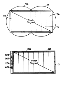
Higher speed is also achieved in x-Si. A 4 x 8 inch
active matrix LCD array can be for~ed from two standard 6- :
30 inch diameter Si wafers Wl and W2 as shown in Fig. 2A. r
Array circuit 25A is formed on wafer W1 and l-inch by 4-
inch tiles TA are transferred from the wafer W1 to the
substrate 14. Note: The transfer may be accomplished
using either a single or double transfer process , as will ~:
WO93/1~91 212 ~12 3 PCT/U593/0i322
be described in detail below. Each tile is registered
against another using micropositioning equipment and
manipulators capable of micron scale accuracy. Similarly, ~ ~
tiles TB are transferred from wafer W2 to form array 25B ~ :
on substrate or common module ~ody 13 (See Fig. 2B~
Logic circuits 40A and 40B and drive circuits 18A,
18B, 20A, 20B are formed on other suitable substrates (not
shown) and tiled and transferred in like manner to common
substrate 13 and registered opposite the arrays 25A, 25B,
as ~hown in Fig. l. Conductive interconnections 5d are
then made between the drive circuits and the individual
pixels 22 and the logic control circuits 40A and 40B. In
this manner, a 1280 by ~024 addres~able array of pixels 22
are formed on the su~stra~e 13 of circuit panel 14. ~ach
pixel 22 is actuated by voltage from a respective drive
circuit 18~ or B on the X-axis and 20A or B on the Y-axis. ~ `
The X and Y drive circuits are con~rolled by signals from
control logic circuits 40A and B. Each pixel l9 produces
an electric field in the liquid crystal ~aterial 23
disposed bel:ween the pixel and a counterelectrode (not
shown) formed on the back side of the color filter plate
16.
The electric field for~ed by pixels 22 cau~es a
rotation of the polarization of light being transmitted
across the liquid crystal material that reæults in an
adjacent color filter element being illuminated. The
cslor filters of filter plate syste~ 16 are arranged into
groups of four ~ilter.elements, ~uch as blue 2i, green 8l,
red 27, and white 29. The pixels associated with filter
elements can be selectively actuated to provide any -
desired color for that pixel group.
A typical drive and logic circuit that can be used to
control the array pixels 22 is illustrated in Fig. 3. ;;:~
Drive circuit 18A receives an incoming signal from control
35 loqic 40A and sends a signal to each source electrode of a ~ ~-
2129~ ~3 ~
WO 93/16491 ` PCT/US93tO1322
-12-
TFT 51 in one of the columns se~ected by lo~ic circuit 40A
through interconnect line 53. Y-drive circuit 20A
controlled by logic circuit 40A energizes a row buss 59 ,~ -
extending perpendicular to column buss 53 and applies a
voltage pulse to each gate G of TFT's 51 in a selected
row. When a TF~ has a voltage pulce on both its gate and
source electrode current flows through an individual
transistor 51, which charges capacitor 56 in a respective
pixel 22. The capacitor 56 sustains a charge on the pixel
10 electrode adjacent to the liquid crystal material (shown ,,
~chematically at 19) until the next scan of the pixel
array 2~. Note: The ~arious embodiments of the invention
may, or may not, utilize capacitors 56 wi'th each pixel
depending upon the type of display desired.
II. Transfe!r ~rocesses
The array circuits 25A and 25B and logic 40A,40B and ,~
drive circuits 18A,18B may be formed and transferred by a
number of processes. The basic steps in a sin~le transfer '
process are: forming of a plurality of thin film Si
circuits on Si substrates, dicing the thin film to form
tiles, and transferring the tiles to a common module
substrate by "tiling." Tiling involves the steps of
transferring, registering the transferred tiles, and
adhering the registered tiles. The Si ~ubstrates are then
removed and the circuits on the tiles are interconnected.
The,double transfer approach, described in detail
below in connection with Figs. 4A 4L is si~ilar except ,~
that the Si-substrate is removed after dicing and the thin
film is transferred to an intermediate transfer body or
carrier before ultimate transfer to the common module
body. -~
Assuming an Isolated Silicon Epitaxy (ISE) process is
used, the first step is to form a thin-film precursor - ,~
structure of silicon-on-insulator (SOI) film. An SOI
,~; 2~ ~123
WO93/1~91 PCT/US93/01322
-13-
structure, such as that shown in Fig. ~A, includes a
substrate 32 of Si, a buffer layer 30, of semi-insulating
~i and an oxide 34 (such as, for example, SiO2) that is
grown or deposited on buffer layer 30, usually by Chemlcal
Vapor Deposition (CVD). An optional release layer 36 of
material which etches slower than the underlying oxide
layer 34 is then formed over the oxide 34.
For example, a silicon oxy-nitride relsase layer,
comprising a mixture of silicon nitride (S3N4) and ~ilicon
dioxide (SiO2) may be a suitable choice. Such a layer
etches more slowly in hydrofluoric acid than does SiO2
alone. This etch rate can be controlled by adjusting the
ratio of N and 0 in the silicon oxy-nitride (SioxNy)
compound.
A thin essentially single crystal layer 38 of silicon
is then formed over the release layer 36. The oxide (or
insulator) 3~4 is thus buried beneath the Si surface layer.
For the case! of ISE SOI structures, the top layer is
essentially single-crystal recrystallized silicon, from
which CMOS circuits can be fabricated.
Note: for the purposes of the pr~sent application,
the term "essentially" single cryctal means a film in
which a majority of crystals show a co~mon crystalline
orientation and extend over a cross-sectional area in a
plane of the film for at least 0.l cm2, a~d preferably~ in
the range of 0.5 - l.0 C~2, or ~ore. The term also
includes completely sin~ e crystal Si. ~ -
- The use of a buried insulator provides devices having
higher speeds than can be obtained in conventional bulk ;
(Czochralski) material. Circuits containing in excess of
1.5 million~ CMOS transistors have been successfully
fabricated in ISE material. An optional capping layer
(not shown) also of silicon nitride may also be formed
over layer 36 and removed when active devices are formed.
~ '
: ' ~ '
212gl2~
WO 93/16491 ` ~C~/US93/01322
-14- -
As shown in Fig. 4B, the film 38 is patterned to
define active cir~uits, such as a TFT ' s in region 37 and a
pixel elec~rode region at 39 for each display pixel.
Note: For simplification, only one TFT S1 and one pixel
electrode 62 is illustrated (Fig. 4H). It ~hould be
understood that an array of 1280 by 1024 s~ch ele~ents can
in practice be formed on a single 6-inch wafer.
A plurality of arrays may be formed on a single six-
inch wafer, which are then applied to the display as tiles
and interconnected. Alternatively, the plurality of pixel
matrices from one wafer can be ~eparated and used in
different displays. The plurality may comprise one large
rectangular array s~rrounded by several smaller arrays (to
be used in smaller displays). By mixing rectangular
arrays of different areas, ~uch an arrangement makes
better use of the total available are~_on a round wafer.
An oxide layer 40 is then formed.over the patterned
regions including an insulator region 48 formed between
the two regions 37, 39 of each pixel. The intrinsic
crystallized material 38 i8 then implanted 44 (at Fig. 4C)
with boron or other p-type dopants to provide a n-channel
device (or alternatively, an n-type dopant for a p-channel
device).
A polycrystalline silicon layer 42 is then deposited
over the pixel and the layer 42 is then implanted 46,
through a mask as seen ln Fig. 4D, with an-n-type dopant
to lower the resistivity of the layer 42 to be used as the
gate of the TFT. Next, the poly~ilicon 42 is patterned to ~ ~-
form a gate 50, as seen in Fig. 4E, which is ~ollowed by a
large implant 52 of boron to provide p+ source and drain
regions 66, 64 for the TFT on either side of the gate
electrode. As shown in Fig. 4F, an oxide 54 is formed
over the transistor and openings 60, 56, 58 are forme~- ~
through the oxide 54 to contact the source 66, the drain -
64, and the gate 50. A patterned metallization 71 of ~ -
,.. . .
WO93t1~91 212 ~12 3 PCT/US93J01322
-15-
aluminum, tungs~en or other suitable metal is used to
connect the exposed pixel electrode 62 to t~e source 66
(or drain), and to connect the gate and drain to other
circuit panel components.
The devices have now been processed and the circuits
may now be tested and repaired, as required, before
further processing occurs.
The next step in the process is to transfer the
silicon pixel circuit film to a common module, either
directly, or by a doubl~ transfer from substrate to~
carrier and then to the common module. A double transfer
approach is tllustrated in Fiqs. 4H-4L. To separate a
circuit tile from the buffer 30 and substrate 37, a first
opening 70 (:in Fig. 4H) is etched in an exposed region of
release layer 36 that occur between tiles. Oxide layer
34 etches more rapidly in HF than nitride layer 36, thus a
larger portion of layer 34 is r~moved to form cavity 72.
A portion of layer 36 thus ~xtends over the cavity 72.
In Fig. 4I, a support post 76 of oxide is formed to
fill ~avity 72 and opening 70, which extendc over a
portion of layer 36. Openings or via holes 74 are then
provided through layer 36 such that an etchant can be
introduced through holes 74, or through openings 78 etched
beneath the release layer 36, to remove layer 34 (See Fig.
2~ ~J). The remaining release layer 36 and the circuitry ::~
supported thereon is now held in place relative to .~ :
substr~te 32 and buffer 30 with ~upport posts 76.
Next, an epoxy 84:that can be cursd with ultraviolet :~ : :
light is used to attach an optically transmissive :; -
superstrate 80 to the circuitry, and layer 36. The ~uffer
- 30 and subs~rate 32 is then patterned and selectively
exposed to light such that regions of epoxy 84' about the
posts 76 remain uncured while the remaining epoxy 84' is
cured (See Fig. 4K)~ The buffer 30 and substrate 32 and
posts 76 are removed by cleavage of the oxide post and
~12~123
WO93i1~91 PC~/US93/01322'~
-16-
dissolution of the uncured 84 epoxy ~o provide the thin
film tile structure 14l, shown in Fig. 4L mounted on
carrier 80.
To form the final display panel, the edge~ of the
carrier 80 are trimmed to coincide with the tile borders.
The nitride release layer 36 is removed by etching.
As shown in Fig. 5A, a plurality of tile ~tructures
141 are then sequentially registered with one another and
adhered to a common module body llO using a suitable
adhesive (not shown). Common module body llO is
preferably patterned with interconnect metallization on
the surface facing the tile structure 141 for
interconnecting individual tile circuitry with each other.
Next, insula~tion and alignment lay~rs, spacers, a sealing
border and ~,onding pads for connections (not shown) are
bonded onto the periphery of the common module body llO.
A screen printing process can be used to prepare the
border. As shown in Fig. 5B, a plate 117 containing the
color filter~ 120 and the counterelectrode (not shown) i~ -
bonded to the periphery thin film circuit tiles 141 with
the sealing border after insertion of spacers (not shown).
The display is filled with the selected liquid crystal
materiaI 116 via a small filling hole or holes extending
through the border. This filling hole is then sealed with ~
25 a resin or epoxy. First and second polarizer films 118, ~;
112 or layers are then bonded to both sides and connectors
(not shown) are added. Fina~ly, a white light source 114,
or other ~uitable light source, is bonded to polarizer
112.
Pixel electrodes 62 are laterally spaced from e~ch
other. Each pixel has a transistor 51 and a color filter
120 or 122 associated therewith. A bonding element or
adhesive 82 and optically transmissive superstrate llO,
such as ~lass or plastic completes the structure. Body
WO93~1~91 21 2 9 12 3 PCT/US93/01322
ll0 is prefera~ly a low temperature glass ~hat can have a
thickness preferably of about 200 to lO00 microns.
In an alternative CLEFT process, thin single-crystal
films, are grown by chemical vapor deposition (CVD), and
separated from a reusable homoepitaxial substrate.
The f ilms removed from the substrate by CLEFT are
"essentially" single-crystal, of low defect density, are
only a few microns thick, and consequently, circuit panels
formed by this process have little weight and good light
transmission characteristics.
The CLEFT process, illustrated in U.S. Patent No.
4,727,047, involves the following steps: growth of the
desired thin film over a release layer (a plane of
weakness), formation of metallization and other coatings,
formation of a bond between the film and a second
substrate, such as glass (or ~uperstrate), and separation
along the built-in-plane of weakness by cleaving. The ; -
substrate is then available for reuse.
The CLEFT process is used to form sheets of
20 essentially single crystal material using lateral _
epitaxial growth to form a continuous film on top of a
release layer. For silicon, the lateral epitaxy is
accomplished either by selective CVD or, preferably, the
ISE process or other recrystallization procedures.
Alternatively, other standard deposition techniques can be
used to form the necessary thin film of essentially single -~
crystal matérial.
~ One of the ne~essary properties of the material that
forms the release layer is the lack of adhesion between -
the layer and the semiconductor ~i~. When a weak plane
has been created by the release layer, the film can be
cleaved from the substrate without any de~radation. As
noted in connection with ~igs. 4A-4C, the release layers
can comprise multi-layer films of Si3N4 and sio2. Such an
approach permits the SiO2 to be used to passivate the back
212912~
WO 93/16491 PCMJS93tO1322 ~,. J
--18--
of the CMOS logic. (The Si3N4 is the layer that is
dissolved to produce the plane of weakness.) In the CLEFT
approach, ~he circuits are first bonded to the glass, or
other transfer ~ubstrate, and then separated, resulting in
simpler handling as compared to, for example, W cured
tape.
The plane of weakness is key ~o obtaining uniform
cleaving between the circuits and the substrate. This
plane may be formed by creating a pattern of carbon on the
surface of the wafer 60 that only a small fraction of the
underlying s~miconductor surface is exposed. These
exposed portions are used as nucleation cites for the
epitaxial fi:Lm. If the growth conditions are properly
chosen, the ~Eilm will grow laterally faster than
vertically, ~eading to laterial overgrowth of the single
crystal film. Within lIm of vertical growth, the film
becomes continuous and of high quality. However, the
carbon layer is weak and, combined with the small fraction
of exposed semiconductor areas where the film is strongly
attached to the substrate, creates a plane of weakness.
This plane can be used reliabily and reproducibly to
separate the film from the substrate. The sub~trate may
be reused. These processes have been used to transfer a
wide range of GaAs and Si circuits to alternative
substrates such ac glas~, ceramic, and other materials,
_ without harm to the active circuitry.
In the ISE process, the oxide film is ~trongly
attached to the substrate and to the top Si film which
will contain the circuits. For this reason, it is
necessary to reduce the strength o~ the bond chemically.
This requires use of a release layer that is ~`
preferentially aissolved with an etchant without ~omplete
separation to form a plane of weakness in the release
layer. The films can then be separated mechanically after
the glass is bonded to the circuits and electrodes.
- ' :
:: :.,
~
~ WO93/1~91 212 312 3 PCT/US93/01322
-19-
Mechanical separation may be accomplish~d by bonding
the upper surface of the Si film to a superstrate, such as
glass, using a transparent epoxy. The film and glass are
then bonded with wax to glass plates about 5 mm thick that
S serve as cleaving supports. A metal wedge is inserted
between the ~wo glass plates to force the surfaces apart.
Since the mask ha~ low adhesion to the substrate, the film
is cleaved from the substrate but remains mounted on the
glass. The substrate can then be used for another cycle
of the CLEFT proces~, and the device processing may then
~e completed on th~ back surface of the film. Note that
since the device remains attached to a superstrate, the
back side can be subjected to standard wafer processing, :~
including photolithography.
One e~odiment of the invention utili~es a
recrystallization sy~tem, shown schematically in Fig. 6 to
form the essentially single crystal Si thin filmO A
sample wafer 134 is formed of poly Si, formed on sio2,
formed on an Si wafer. A capping layer 138 is formed over :~
20 the poly Si. The wafer temperature is then elevated to :
near the melting point by a lower heater 130. An upper
wire or graphite strip heater 132 i~ then scanned across ~ :~
the top of the sample 134 to cause a moving melt zone 136
to recrystallize or further crystallize the
polycrystalline silicon. The lateral epitaxy is seeded
from small openings formed through the lower oxide. The
resultant single crystal film has the orientation of the
substrate.
A number of unique devices and circuits have been
formed using the above processing techniques. These
techni~ues have been used to transfer CMOS acti~e matrix
LCD circuitry from ISE wafers to glass, and have yielded
excellent displays with single crystal Si active matrix
circuits. Silicon circuitry has been transferred to glass
and shows no important changes in transistor
~12~23
WO93/16491 ;; PCT/US93/01322
-20-
charcteristics after transfer. The technique has also
been proved with III-V compound semiconductor circuits.
For example, GaAs and AlGaAs monolithic series-connected
photo~oltaic energy converters ha~e been made for power
down a fiber application that yield exceptio~al
performance. Also, two-dimensional multiplexed AlGaAs LED
arrays (with o~er 32K pixels) have been made by transfer
and two-sided processing and exhibit extremely high LED
density as well as performance. The development of this
broad range of Si and III-V circuits indicates the general
applicability of the transfer process to a wide range of
devices and circuits.
III. Alternate ~dhesion and Transfer Processes
FigsO 7A-7D illustrate an alternate preferred double
transfer process for adhering a~d transferring tiles of
circuits of thin films of silic~n to a common module body.
The starting structure is a silicon wafer 118 upon which
an oxide layer 116 and a thin film of poly-Si, A-Si or x-
Si 114 is formed using any of the previously described
processes such as ISE or CLEFT. A plurality of circuits,
such as pixel electrodes, TFT's, Si drivers and Si logic
circuits, are then formed in the thin film. Fig. 7A shows
three such wafers, I, II, III. In wafer I, logic circuits
40 are formed. In wafer II, pixel electrodes 62 and TFT's
51 are formed. In wafer III, driver circuits 20 are
formed~. A wafer,~ or indiYidual tiles diced from the
wafer, is attached to a superstrate transfer body 112,
such as glass or other transparent insulator, using an
adhesive~120. Preferably the adhesive is comprised of
commercially available epoxies. .
~ he wafer, or tile, is then cleaned and the native
oxide 118 is etched off the back surface~ Depending on
the thickness of the wafer, it may take up to 5 hours to
etch the Si 118 and oxide 116 layers. The solution etches
~ WO93/1~91 2 1 2 9 1 2 3 PCT/US93/01322
silicon very rapidly, i~e. 2 ~o 3 microns/min., and
uniformly if the wafers are held horiæontally in the
solution with the etching surface face up. The acid has a
very low etch rate on oxide, ~o that as the substrate is
S etched away and ~he buried oxide is exposed, the etching
rate goes down~ The observer can monitor the process and
to stop the etch in the buried oxide layer 116' without
punching through to the thin silicon layer 114 above it.
Wafers up to 25 mils thick and oxides as thin as 4000A
have been successfully etched using thiis process. An
alterna~i~e etchant is hydrazine, which ha~ a much higher
etch rate selectivity or ethylene diamine pyrocatacol
(EDP).
When thle silicon is completely gone, the vigorous
bubbling, which is characteristic of ~ilicon etching
abruptly stops, signalling that the etching is complete.
The thin films 114 transferred to the respective
glass super~trates 112 are now rinsed and dried. If not
already provided with circuits 40, 5l, 62 or 20, the films
114 can be backs~de circuit processed, if desired.
After all the necessary circuits are formed, as ~ ;
above, on transfer bodies 112, they may now be diced and
tiled onto a common module body 13 (Fig. 7D) to perform a
combined function, such as an AMLCD.
The lo~ic circuits 40 of transfer body 118 in col. A, ~ ~
Fig. 7C, are transferred to the border of module body 13, ~ ~ -
while the driver circuits 20 fr~m the transfer body 118 in ~-
col. C, Fig. 7C,~are dispo~ed on the border between the
logic circuits 40A and 40B.
Tiles of pixel electrodes 62 and TFT' s 51 are formed
by dicing or etching and are registered with respect to
each other and pre-ormed wiring 50 on module body 13, as
shown.
After all the circuits are registered and adhered to
the module body, the transfer body 118 and the epoxy 120
2129123
WO93/16491 PCT/US93/01322
-22-
is removed using a suitable etchant, such as HF for the
case of a glass transfer body.
Interconnection of circuits is achieved during
registration or by direct laser writing where necessa~y.
Also, if desired, the film can be transferred to another
substrate and the first glas~ superstrate and adhesive can
be etched off, allowing access to the front eide of the -~
wafer for further cir~uit processing. ~ ~
Figs. 8A and 8B illustrate an alternative one-step ~;
silicon thin film transfer process in which GeSi i8 used
as an intermediate etch ~top layer. In this process, Si ;
buffer layer 126 is formed on an x-Si substrate 128 ;~
followed by a thin GeSi layer 129 and a thin A-Si, poly-
Si, or x-Si device or circuit layer 132; using well-known
CVD or MBE growth systems.
The layer 132 is then IC processed in the manner -~
previously described in connection with Figs. 4E-H, to
form circuits, such as TFT's 200 and pixel electrodes ~02
(Fig. 8A). Next, the processed wafers, or tiles from the
wafer, are mounted on a common module glass (or other)
support 2~0 using an epoxy adhesive of the type previously
mentioned in connection with Figs. 7A-7B. The epoxy fills
in the voids formed by the previous processing and adheres
the front face to~the superstrat~ 280.
Next, the original Si substrate 128 and Si buffer l26
are removed by etching, which does not affect the GeSi
layer l2g~(Figs.~8B). Finally, the GeSi layer 124 is
removed by brief submersion in a suitable etch.
I~. Pressure Sensor Embodiment
Figs. 9A-9B illustrate an alternate embodiment
related to isolating and transferring circuits. In a
representa-tive embodiment, a method of fabricating
pressure sensing transducers on a glass substrate is shown
in Figs. 9A-9B and described hereinafter. The transducer
~ 1 ; '
W093/1~91 212 912 3 PCT/US93/01322
-23-
circuit opera~es by sensing a cha~ge in the resistance of
the p-region 904 in response to pressure applied to the
circuit. This resistanc~ change may be sensed by an
ohmmeter coupled across contacts 912 and 912 and
calibrated and converted in~o a pressure sensor to ~erve
as a strain gauge. The starting structure is shown in
Fig. 9A. An SOI wafer is provided which consists of an Si
substrate 900 beneath a buried oxide layer 902, upon which
is formed a single, or nearly single, crystal Si layer
904. A blanket implant of boron ion~ is made to make the
Si layer a p-type conductor. A thin ~loooA) blanket
protective/mask layer of oxide (Sio2) (not shown) is then
formed over the structure. (Note Fig. 9A ~hows the
structure after processing). S ~le, or nearly single,
islands of x-Si are then formec ~r y applying photo-resist
over the oxi.de structure and e~_hing the oxide and silicon
904 between islands to align the edges of the islands ~;
parall~l to the ~llO] plane. Photo resist is applied
again and contact openings formed to contact regions 9lO
and 908, which are then implanted with a high dose of
boron ~ons to form P~ type conductivity regions. A
protective oxide layer 906 i5 then formed over the island.
Aluminum contact pads, 912 and 913 to the contacts 908,
~910 are formed in openings provided through oxide 906.
The pressure~transdu~er circuit of Fig. 9A is now ready
for transfer to a temporary glas6 cubstrate. ~
After the circuit 918 is formed, the circuit is
~ransferred to a temporary ~ubstrate 920 using a removable
epoxy 922. The silicon sub~trat~ 900 is etched away. ~
30 Then: using a photoresist and mask the initial oxide layer
902 is etched around the periphe~y of the circuit 918
leaving the circuit free to be inverted and transferred to
2~29~23
W093/l64gl . Pcr/usg3/0l322 ¢~?
-24-
the glass substrate 920 and releasibly bonded thereto
using the removable epoxy 92~ from which it can be
transferred and bonded to a module for general sensing,
including te~perature, pressure, acceleration, and 50
forth, all under microproceæsor ~upervision, to make a
high speed process controller.
Figs. lOA and 108 illustrate an alternate transfer
process in which the initial oxide 902 is etched a~out the ~;
periphery of each circuit ~18 using a conventional photo-
resist and ma~k technique. The Si substrate 900 is also
etched locally which preferentially etches Si to reveal
the ~ plane. A nitride layer may be added such that
the etchant does not etch the aluminum. Etching of the Si
substrate with hydrazine undercuts the circuits 918
forming a cavity 930 under the cirouits and leaving a
bridge structure 934 between circuits 918 and the
su~strate. ` ` ~ ~
When it is desired to remove one or more circuits ~ ;
918, a vacuum wand may be used to seize one or more
circuits and break the bridge to remove the circuits which
may then be transferred along with other circuits to a
common module substrate and aligned and interconnected
with other circuitry to perform an overall function as
previously described. Alternatively, other techniques
such as laser a~lation can be used for removing the-
circuits from the ~ubstrate.
Fig. lOB is a top-plan view of Fig. lOA before
substrate 900 is etched where the bridges 934 are shown.
The bridges make an angle of about 22~ relative to the
long s ~ etry axis of the circuit 918.
~ :
f W093/1~91 ~ 2 ~ 2 912 ~ ` PCT/US93/01322
V. Three-Dimensional Circuitry :
A. 3-D C rcuit ~r~hitectu~
Other embodiments of the present invention relate to
the formation of three-dimensional circuits. In forming a
two-layer three-di~ensional cirauit, a ~irst circuit 1000
(Fig. llA) ~ormed in a sili on layer 1002 on an oxide
layer 1004 on an Si substra~e 1001 is transferred onto a
glass superstrate 1006 as s~wn in Fig. llB. More
specifically, the singie-transferred circuit 1000 is `
transferred to a glass superstrate, coated with amorphous
silicon, by any of the aforementioned transfer methods and
bonded to the glass wi~h an adhesive or ~poxy 1008.
Referring to ~ig. llC, a second circuit ~010 i5 double~
transferred to a glass or diamond substrate 1011. The ;-
circuit 1010 is preferably formed in a layer of silicon
1012 on an oxide layer 1014, and i~ bonded to the
substrate by a layer of adhesive or epoxy 1016.
Referring to Fig. llD, a three-dimensional device is
formed by bonding the single-tran~ferred circuit ~000
(Fig. llB) on top of the double-transferred circuit lolo
(Fig. llC) using thin, uniform adhesive 101~. Since the
circuits can be observed through the glass ~ubstrate 1011,
_ they can be aligned using a microscope or a contact or
proximity-~aligner as routinely done in photolithography
where a mask is aligned on ~op of a ~ilicon circuit in
process or by other appropriate micropositioning tools or
techniques.
~ After bonding, the superstrate 1006 is removed as in
a double-transfer process and the~adhesive 1008 is removed
in oxygen plasma. This leaves ths front surface of the
top circuit 1000 exposed. The bottom circuit 1010 is
WO93tl~91 212 912 3 PCT/US93/01322 ~
-26
buried beneath the adhesive layer 1018. In order t~ make :~
connections between the layers of circuits, openings or
via holes (not ~hown) are defined by appropriate etchants
in order to expose contact areas on the two circuit
layers. All of the oxide i~ etched in buffered HF using
photoresist a~ a mask while the adhesive can be etched in .:
oxygen plasma or by reactive ion etching (RIE) using the .~
previously etched oxide as a mask. Once these via holes ~ :
have been opened in the bonding layer, they can be filled ;~
with metal in order to make the contact from layer to
layer. The layer to layer i~terconnections are explained ;:~
in detail below. The adhesive layer between the
superposed circuits must be kept very thin, 1-25 microns,
preferably 5 microns thick to facilitate layer to layer
contacting. The proce~s can be repeated to add additional
layers to the device.
The performance characteristics of each circuit in a :
three-di~ensional structure are related to the thermal ::
conductivity o~ the medium in which the circuit is ;
disposed. Figs. 12A-12B show performancè curves of a
lower MOSFET circuit o a three-dimensional device (such
as in Fig. llD) and the corresponding curves for a similar
device after double-transfer and before three-dimensional
mounting (such as in Fig. llC). The graphs of Figs. 12A- ~ ~ :
25 12B show that the trans~onductance and the drive current
are higher when the circuit is buried under epoxy (Fig.
llD) than when it is exposed to ~bient air (Fig. llC).
This effect can be explained by a higher thermal
conducti~ity of the epoxy with reqpect to air which ' ~
30 results in a reduced heating effect for the circuit buried ~ :
in epoxy (Fig. llD). It is noted that carrier mobility 1 -
decreases as the:temperature of the circuit increases and
~ ~W~3/16491 2 1 2 9 1 2 3 PCT/US93/013~2
-27-
that performance is directly related to carrier mobility.
Thus, ~urrounding circuits in highly conductive epoxies
provide lower device temperatures leading to improved
performance characteristics. These epoxies can be filled
with particles of thermally materials ~uch as diamond
aluminum nitride, silicon carbide, and other conductive
compounds. There are many available thermally ~ ~`
conductive/electrically in~ulating epoxies.
An advantage o~ this approach is the capabil~ty to
integrate heat sink layers within the stack. Heat
difisipation is an important problem in 3D architectures,
and a capabili~y for insertion of heat conducting layers
between active electronic layer~ is advantageous. These
layers can have much higher thermal conductivity than can
be attained in Si or other semiconductors that may be
envisioned ~or heat transfer. `~
One significant aspect in the formation of three-
dimensional circuits involves interconnecting the layered
devices. It is noted that in such circuits, the epoxy
disposed between the device layers may be spun to obtain a
thickness of a few microns. Alternatively, other known
techniques can be employed to obtain a thin, uniform layer
of epoxy. Fig. 13A is a sectional view o~ Fig. llD taken
along the line A-A and shows the }ower contact area 1020
25. forme~ via metalization in the plane of the silicon layer
1012 for providing electrical connection to the circuit
1010 (Fig. llD). Similarly, upper contact areas (not
shown~ are formed directly above the lower areas in the
plane of the silicon layer 1002 and are electrically
connected to the upper circuit 1000 (Fig. llD). Referring
to Fig. 13B, the upper and lower areas (1024, 1020) employ
an optional poly-Si layer for strengthening the areas for
212~123
W093/1~91 PCT/US93/01322
-28-
contacts. Via holes 1022 are ~ormed through the upper
conta~t areas 1024 to gain access to the lower contact
areas 10200 The etching to form the via holes with high
aspect ratio is performed by an RIE technique. Electrical
contact betwee~ the upper and lower devices is made by
filling the via holes l022 with an electrically conductive
material such as tungsten or aluminum.
Another ~ignificant aspect of three-dimensional
circuits involves shielding device layers to avoid
undesirable electrical or magnetic interference between
devices. Réferring to Fig. 14, ground planes 1026 are
positioned bstween device layeræ 1028 and 1030 to prevent
electrical interference. These conductive ground planes
1026 can be made with a metal or by IT0 deposition on the
suxface of the oxide layer 1032 opposite the device 1034.
Alternatively, the ground planes can be formed with an ~ ~-
electrically conductive epoxy or with a highly doped
silicon layer taking the place of a device layer in the
stacked structure.
A benefit of using transfer technology to form a
multilayer stack is attained if superior radiation
resistance and low weiyht are desired. ~he removal of the
substrate decreases the probability of single event upset
__ and reduces the weight, but also important is the
potential for utilization of high-Z radiation shielding-
~materi~al at the outside surfaces of the device. This
shielding can protect many layers of stacked circuits with
much less increase in weight than is needed for a 2D
geometry. Thus, there are important benefits for space
applications in which radiation resistance and weight are
important factors.
~ .
. ~ ~
~ 'WO93/1~91 212 ~ ~ 2 3 PCT/~S93/01322 ~ ~
-29-
A further benefit of the proposed technology is that
the multi-layer circuit may be màde tamper resi~tant.
This benefit is particularly important for the prevention
of rever~e engineering for proprietary circuit~. In a 2D
circuit, the die can be removed from the package and
examined by microanalytic techiques. However, a 3D
circuit can be formed in such a way that separation of the
layers is not only c ffic~lt, but also highly destructive,
so that separation of the layers would not yield
meaningful pa~terns or useful reverse-engineered data.
Speed advantages can be attained by using a 3D
approach. For example, in a memory comprising stacked 2D
circuits access time can be reduced because the transit
distance for address signals is shorter than a compar~ble
tilted planar 2D memory. As another example by using a 3D
addressing scheme for a true 3D ar~hitecture, access time
may be reduced to an even lower level.
Trans~er of circuits lnto a 3D architecture can also
permit the integration of high speed GaAs analog signal
processing circuitry (NMICs) with silicon circuits. This
permits the integration of microwave circuits with high
speed highly dense Si circuits. Such versatility may not
be easy to obtain with other approaches. Transfer is also
applicable to digital GaAs circuitry.
- 25 Finally, thé transfer approach, makes po~si~le the
use of optoelectronic circuits and devices. These ~-
circuits can be used for opti~al computing, optical I/O,
or optical interconnects~between circuit planes in the 3D
structure. Other uses of`optoelectronic devices or
circuits can be integrated relatively easily if a need for
these devices arises.
W093/1~91 212 9 12 3 - ` PCT/US93/Ot322~f~
-30-
This technology makes possible the vertical .
integration o~ memory layers, leading to new circuit :
architectures. Specific advantages include the following: :
:~ ~
- Extremely rapid access time, ~:~
- New memory architectures that are more ~ . :
compatible with neural network memory models, ..
and -
- Compatibility with optical processing and
optical addressing of the memory.
~ ~.
These advantages are a result of the capability not
only to i~tegrate connections between layers, but also to ~. :
interpose optoelectronic devices and circuits within the
layers. Thus, the proposed technology may form the basic .
building block of an entirely new type of circuit
15 architecture. . ~ ~
, ~, ', ,:
B. 3-D Devlce Formation :
In accordance with the present invention, a
fabrication process comprising single and double transfer
steps and a backslde processing step can be employed to
provide various 3-D devices. The fabrication process
includes the formation of circuits in a Si film of an SOI . .
structure, adhering the circuits to a superstrate and
removal~of the substrate. At this point~ the silicon
circuits have been.single-transferred and the backside of
25 ~the silicon circuit layer is exposed. Backside processing
can be performed.so long as the processing is compatible
with the selected adhesive. After backside processing is
performed, the silicon circuit layer is transferred to a
glass substrate (double-transfer). . ~:~
.::
f wo 93~1~91 2 1 2 9 1 2 3 PCT/US93/~1322 ~
-3~
In one preferred embodiment, a double gate MOSFET can
be formed in accordance with the above-described
fabrication process. Firsk, a standard MOSFET device 1050
ha~ing a drain (D~, a gate (G1) and a ~ource (S) (Fig.
5 15A) is formed by an suitable method such as described
previously herein. The next step in the process is to ~;
transfer the device film 1052 from its substrate 1056 to a
superstrate for backside processing. A sin~le transfer
approach is shown in Figs. 15B-15D. Referring to Fig.
10 15B, an epoxy lOS8 is used to attach an optically
transmissive superstrate 1060. In a preferred embodiment,
a glass superstrate coated with A-Si is employed with a
two-part epoxy. Once the front surface of the film 1052
has been bonded to the superstrate 1060, the substrate
1056 is etched. As shown in Fig. 15C, the etchant rapidly
removes the silicon substrate 105~ with the oxide layer
1054 serving as an etch stop. The etch rate 6electivity
of 200:1 for ~ilicon versus thermal silicon dioxide allows
the use of very thin oxide layers leaving the device 1050
protected from the etchant.
After single transfer, using an opposite polarity
gate mask (not shown) the oxide layer 1054 is thinned down
to a few hundred angstroms ( 500 ) along the channel
region 1062 (Fig. 15D).~ An alternative method of
pr~viding a thin oxide~layer adjacent the backside-of the
MOSFET device 1050 is illustrat-d in Fig. 15E. Once again
using a mask (not shown~, the oxide layer ~long the
channel region 1062 is etched away to expose the backside
of the device 1050. Next, a thin oxide layer 1063 (-500
) can be deposited in-the region 1062.
A second gate (G2) is then formed over the thin oxide
layer 1063 and electrically connected to the first gate
212~l 23
WO93/1~91 PCT/US93/01322
-32-
(G1) as follows. Referring to Fig. 15F, whîch is a cross-
sectional view o~ the structure shown Fig. 15E a contact :~
hole 1065 can be opened through the thinned oxide, and a
gate material (1066) can be deposited ~nd etched to form a
second gate (G2) 1064 which is electrically connected to
the first gate (Gl~. This dual gate configuration serves
to practically double the drive current for the MOSFET
1051 since the device has two channels. Referring to Fig.
15G, the dual gate MOSFET 1051 may be transferred again
and bonded with epoxy 1067 to a permanent substrate 1068
such as glas~s.
In another preferred embodiment, a 3-D double-gate
MOSFET inverlter 1070 can be fabricated such that the n~
channel and ~p-channel MOSFETS share the same body with
their channe:ls disposed on opposite sides thereof. The
fabrication ~sequence for providing a double-gate inverter
is shown in ~Figs. 16A-16J. Referring to Fig. 16A, the
device 1070 includes an n-channel MOSFET 1072 with a gate ~ ~
(Gl), source (S1) and drain (D1) and a p-channel MOSFET :~:
1074 with a gate (G2), source (S2) and a drain (D~).
Referring to ~ig. 16B, the shared region 1076 includes the
n-channel 1078 and the p-channel 1080 which are disposed
on opposite sides of the region. More specifically, the :
channel for the n-channel MOSFET is ~isposed along the top
interface 1081 of the shared region and the channel for
the p-channel MOSFET is disposed along the bottom :
interface 1082 of the shared region.
A series of plan views illustrating the processing ~ ;
steps employed for ~abricating a dou~le gate MOSFET
inverter are shown in Figs. 16C-16J~ Fig. 16C illustrates
the channel doping for the p-channel MOSFET. A
photoresist and a mask are positioned over the patterned
~ `W093il~91 2 1 2 ~ 1 ~ 3 PCT/US93/01322
-33-
silicon islan~ 1084 and phvsphorous (or other n-type ~ -
dopants) is implanted into the area 1086 with a projected
range (~) near the bottom interface 1082 (Fig. 16B). The
implant i6 such that the pho~phorous concentration at ~he
S bottom interface is about lo16 c~3~ F~g. 16D illustrates
the channel doping ~or the n-channel MOSFET. Using a
photoresist and mask, boron (or other p-type dopants) is
implanted in the area 10~8 with an Rp near the top ~
interface 1081 tFig. 16B). The implant preferably
produces a boron c~ncentration at the top inter~ace of
about 4 x lol6 cm3.
Fig. 16E illustrates the formation of the channel
stop 1083 (Fig. 16B~ for the n-channel MOSFET. A
photoresist and mask are positioned over the silicon
island such that boron is implanted into the regions 1089
with an ~ in the in the middle of ~ilicon. This implant
is such that the average boron concentration in the middle -
o~ the silicon is about 4 x 1016 cm3. Fig. 16F
illustrates an edge implant for the n-channel MOSFET. To
avoid the effect of sidewall parasitic transistors, the
corner regions 1077 (Fig. 16A~ extend beyond the gate
material preventing the gate from contacting the sidewall
; of the silicon island to form a sidewall transistor.
~Further, these corner regions are heavily doped to
minimize sidewall transistor ef~ects on the double-gate
inverter. Using a photoresist ~nd mask, boron (or other
p-type dopant) is implanted into the areas 1090 with an Rp
near the top interface. The implant preferably produces a
boron~;~concentration at the top interface of about 5 x 10¹⁷
cm.3 ~
Referring to Fig. 16G, the gate (G1) and the contact
area 1094 are then formed for n-channel MOSF~T. Next, the
,,; ~.
.
:
212~ ~3
WO93/1~91 . PCT/US93/01322
-34~
source/drain doping is performed for the n-channel device.
Using a photorssist and mask, arsenic (or other n-type : :
dopants~ i8 implanted, self-aligned with the gate (Gl),
into the area 10g6 with an ~ near the top interface and
an arsenic concentration of about 1o20 cm3. Fi~. 16H
illUstrates thë formation of the channel stop 1079 (Fig.
16B) for the p-channel MOSFET. Using a photore~ist and
mask, phosphorus (or other n-type dopants) is implanted,
self-aligned with the gate (Gl), into the area 1097 with
an ~ near the top interface 1081 (Fig. 16B) and a
phosphorus concentration of abo~t 8 x lO16 cm3. Next, the
source/drain doping is performed for the p-channel MOSFET. ~ :~
Again using a photoresist and mask, boron i~ implanted :~;~
into the areas 1098 with a ~ in the middle of the silicon :
and an average boron concentration of 102 cm3.
Next, the gate ~G2) is formed for the p-channel
MOSFET and electrically connected to the gate (G1).
Referring to Fig. 16J (which is a sectional view of Fig.
16A taken slong the line J-J), the double-gate MOSFET is
single transferred to a temporary superstrate 1100 and
attached to the superstrate by an adhesive or epoxy 1102. : ~
Then, the oxide layer 1104 upon which the device is ::~ ::
disposed is Qelectively etched using a photoresi t and a :
mask to open two areas 1106 and 1108. Next, the gate (G2) :
25 is formed i~ the area 1106 by metalization as well as the :~
contact path~lll0 to the contact area 1094. After ::
metallization, the two gates are electrically connected. -
In another preferred embodiment, a three-dimensional
inverter, i8 formed with a pair of MOSFETs which are
vertically stacked as shown in Fig. 17D. The fabrication
process for the three-dimensional inverter is shown in
Figs. 17A-17D. Referring to Fig. 17A, an n-channel device ~-
~ WO93/1~91 212 912 3 PCT/US93/01322
-35-
1200 is formed in single cryqtal silicon 1202 on an oxide
1204 over a substrate (not shown). ~fter a double .-.
transfer, the device 1200 is attached with an adhesi~e or
epoxy 120~. A pa~sivation oxide layer 1210 is deposited
over the device 120.
Referring to Fig. 17B, a p-channel device 1212 is
separately fabricated in single crystal silicon 1214 on an
oxide 1216 on a substrate (not shown). An oxide layer
1224 is deposited over the p-channel device 1212 for
10 passivation, and single transfer is performed such t~at ~ ~
the device is attached to a ~uperstrate 1218 by an :`
adhesive 1220. The p-channel de~ice 1212 is then
attached to the n-channel devi~e by an adhesive 1222
formi~g a stacked structure (Fig. 17C).
Next, an oxide layer 1224 i~ deposited over the p-
. .
channel devi.ce 1212 for passivation. Referring to Fig.
17D, vias 1226 are then formed to access t~e gate, source
and drain regions of the upper device 1212 and the buried
de~ice 1200. A metal layer 1228 is deposited and
patterned to form electrical interconnects, for the
stacked inverter structure 1230. It is noted that the ~:
interconnection of the respecti~e gates is made in a plane
parallel to the figure such that the vias are not shown.
: In yet another preferred embodiment, a vertical
bipolar transistor is ~abricated in accordance with the
principles of the pres:ent invention. :The fabrication ;~ :~
process sequence is shown in Fi~s. 18A-18H. 8egi~ning
with a silicon film 1240 on an oxide I242 on a substrate
1244~(Fig. 18A), the silicon is patterned into device
regions as shown in Fig. 18B. Next, a deep implant of an
n-type dopant 1241 is performed for producing an n-doped
collector region 1250. Re~erring to Flg. 18C, the device
.,
..:
W093/1~9121 29 ~ 2 3 PCT/US93/01322'~
-36-
region is doped with boron or other p-type dopants 1243
for providing a p-typ base region 1251. Referring to
Fig. 18D, the silicon is doped with an n-type dopant 1244
to provide an n+ emitter region l245. Next, the silicon
is heavily doped with an n-type material 1247 to provide
an n+ collector region 1248 (Fig. 18Ej.
The collector, emitter and base contacts 1252 can be
formed (Fig. 18F) and the device can be transferre~ to a
superstrate 1254 (Fig. 18G). The device is attached to
the superstrate with an epoxy 1256 and inverted for
further processing. To t~at end, a portion of the oxide
layer 1242 is etched forming an opening 1258 at the back
of the silicon layer. Next, a metal layer 1260 is
applied over the exposed backside of the silicon film and
sintered (Fig. 18H). A high temperature implant (-450~C)
can be impl~mented prior to metalization to produce an n+
buried conductor layer 1250 provided that a high
temperature epoxy is used.
Three dimensional circuits can also be fabricated in
III-V semiconductor materials, with appropriate release
layer material and etchant. For an AlGaAs/GaAs device, an
AlAs release layer is preferred. For an InP device, an
InGaAs release layer is preferred. AlAs is preferentially ~`~
etched by HF acid, while InGaAs i5 preferentially etched
by sulfuric/hydrogen ~eroxide and water ~olution. The
process can~lso be extended to II-VI semiconductor
circuits. -
For example, the fabrication of III-V circuit array,
in accordance with the invention, will be described with
reference *o Figs. l9A-D. It begins with the epitaxial
growth of the required heteroepitaxial layers of AlGaAs
and GaAs layers on a GaAs or Ge substrate. In the case of
WO93/1~91 2 1 2 9 1 2 3 PCT/USg3/0l322
the GaAs substrate 312, an optional layer 314 of AlAs is
formed between ~he active AlGaAs layers 31Ç and the
substrat~ 312 to facilitate su~strate removal by the etch-
off method. ~he AlAs forms an etch stop layer.
Alternatively, the X-Y array can be removed from the
substrate by a CLEFT process (See U.S. Patent No.
4,727,047 issued February 23, 1988 to Fan et al.) or
chemiçal epitaxial lift~off. In the case of Ge
substrates, a layer of AlAs can be used as an etch stop,
but ~lAs is not really necessary, since the Ge substrate
can be dissolved in ~22 without harm to the AlGaAs active
layers. Fis~ l9A shows the epitaxial layer structure to
comprise an active GaAs (or AlGaAs) layer 366 formed by
OMCVD~ A pattern of contact pads ll9 and busbars ~not
shown) i8 formed by photolithographic techniques,
evaporation, and/or electroplating on the front surface, :
as shown in Fig. l9B. Next, the circuits 313 are isolated ;: ~
by etching part way into the epitaxial layers 316, as ;: :
shown in Fig. 198. This step is not absolutely required
at this point, however, it simplifies a later etch step in
the process.
The next stage of the process consists of bonding of ..
the wafer to a support 380, such as glass, ceramic, or
thin stainless steel. If the support is transparent to ~ ~ :
infrared radiation, downstream front-to-back alignments
: are facilitated,`but the alignments can also:be carried :~
out by careful registration to the support edges. The ~ -
processed front side is bonded to the upport 380 using a ~ :
suitable adhesive (not shown) (Fig. lQC). After the
support 380 is attached, the wafer or substrate 312 is :
etched off (or cleaved off~ leaving the thin film 316
attached to the support 380, as shown in Fig. l9D, in
2~2~123
WO93/1~91 . ` PCT/US93/01322~ ~
-38- :
which the structure has b~en flipped over onto the 8upport
to expose the backside B for processing.
once the backside is exposed, any remaining non~
essential material is removed from the back by selective
etching in HF to expose a clean Ga~s contact layer B. The
backside contacts 321 and busbars ~21x are now
photolithographically patterned and electroplated or
evaporated onto the contact regions 316'. - `
As shown in Fig. 20, the front ~ackside proc~ssed `
circuit array 330 may be mounted directly to a silicon
wafer 323 i~ a precise location 310 with X and Y silicon
driver circuits 320 and 322 formed in wafer 323 and
coupled to the X and Y bonding pads 324 and 326,
respectively. Bonding of array 330 to wafer 323 may also
lS be accomplished by having the contact pads 326 replaced by
cantilevered bars that extend over to pads on wafer 323
and which can be trimmed to form circuit bonding pads.
Note that in the first step of the backside process,
.. _ . .
undesired epitaxial layers are removed; these layers are ~ ~-
20 present to initiate the epitaxy, or may be buffer layers ` ;~
that are not needed in the final device. To make their
removal simple, as AlAs etch stop layer (not shown) may be
provided in the epitaxy between these layers and the
epitaxial device structure. The layers can then be
~25 removed in etches that stop at AlAs, ~uch at the well
known PA etches. At a pH of about 8, these etches
dissolve GaAs 1000 times ~aster than AsGaAæ. After the
etch stops at the AlAs, the AlAs can be removed in HF or
HCl. ~ A
In the process described above, the backside of the
substrate is provided with multiplex-compatible
metallization to contact the back of each pixel. Note
; WO93/1~91 ~ PCT/US9~/01322
-39-
that this type of processing requi~es front-to-back
alignment. The pixels are then separiated by a mesa etch.
Because ~he films are only about 5 microns thick, the mesa
etch is straightforward and quick. The etching may be
accomplished with either wet or dry processing. At this
point, the exposed semiconductor may be coated with
dielectric to prevent association.
As shown in Fig. 21 a detector 450 and LED array 300
can be stacked into a hybrid assembly comprised of a top
thin film I.R X-Y detector array 450 affixed by light
transparent glue to lower thin film LED array 300 mounted
on glass su]bstrate 620. A glass lens 460 is affixed to
the top surface of detector 450 and heat transfer openings -~:
460 provideid as necessary for cooling purposes. The
15 entire etructure can be quite thin ~l ~il~, with the ~:
electronics 470 provided around the periphery.
Ultimately, ~he monolithic thin film array can be mounted
on ordinary glasses for image enhancement of visible ~ -~
light, as well as for display of data superimposed on
video images.
The applications of the device of Fig. 21 include
military night vision systems,-range finders, advanced
military avionics, personal communications systems, and
medical systems in which real-time i~age enhancement is
usefu~
As ~hown-schematically in Figs. 22 and 23, X-Y arrays
can also be used to form a multicolor display. To make
such a display, individual X-Y array labelled LæDl~ LED2
and LED3, are formed from two or ~ore ~fferent epitaxial
stru~ture. The prima ~ difference ..~ '~h8 ~tructure is in
the acti~e layer material 161, 16~ d 163, which must
have different band gaps to create different colors. For
.
2~ 2~23
WO93/1~91 ~ PCT/US93/01322
-40-
example, red 163 can be created with AlGaAs, and green 162
can be created with InAsGaP. The top device ~EDl may be a
blue LED formed of II-VI material, such as ZnSe, ZnSSë or
a group IV alloy such as SiC.
The arrays must be ~tacked with the larger bandgap
LEDl closer to the observer. ~he material with the larger
bandgap will be transparent to the radiation from the
smaller bandgap. Thus, in this way, the observer ~ill be
able to ~ee both colors.
~he creation of the stack of three LEDs 1020 is as
follows: first, the three separate LED arrays LEDl, LED2
and LED3 are ~ormed, as previously described. Next, they
are stacked together with glass 600 between them. ;~
Transparent glue or epoxy 400 is used to bond the
stacks on top of each other. TAe upper and lower bonding
pads P1 and P2 on each LED are laterally staggered with
respect to other LEDs, so that individual LED pixels may
be addreæsed (See plan view Fig. 23)~
Integrated circuits fabricated on other materials can
also be stacked into 3D circuit modules using a transfer
process as described above. The circuits can be
fabricated in II-VI or I-VIII compounds or in diamond thin
films. In addition, a 3D circuit module may comprise
stacked layers of differing materials. For example, GaAs
circuits can be stacked adjacent t~ Si circuits
Fig. 24A illustrates a 3D circuit stack
interconnected by conductive material. The circuits
layers 1410, 1410', 1410 " are stacked onto a carrier
substrate 1401. The circuit layers 1410, 1410', 1410''
are fabricated separatedly using an above-described
transfer process. The circuit layers 1410, 1410', 1410''
are adhered to the carrier substrate 1401 and to adjacent
` WO93/1~91 2 ~ 2 9 1 2 3 PCT/US93/01322
-41-
circuit layers by interleaved thin-film epo~y layers 1420,
1420', 1420''. As each layer is transferred interconnects
1414 are formed by patterning and etching the epoxy layers
1420', 1420 " to form vias and then depo~iting a thin-film
metallization layer into ~he vias. To promote thermal
conductivity, away from the circuitxy the epoxy may be
impregnated or supersaturated with a thermal conductive
material, such as diamond. -
In addition to metal contacts through vias, stacked
layers of circuits may employ contactless interconnects.
Fig. 24B is a schematic diagram of stacked circuit layers
comprising contactless interconnects~ Shown are two thin ~-
film circuit layers 1410, 1410" interconnected within a
thin film circuit module having a plurality of thin film
circuit layers. Each interconnected circuit layer 1410,
1410 " comprises a contactless coupling element 1415,
1415' registered to each other. The plurality of circuit
layers are transferred and adher~d by interleaved epoxy
layers 1420, 1420', 1420 ".
Any intervening circuit layer 1410' must be patterned
and etched to form vias through that layer. Pxeferably,
the intervening circuit layer 1410' is patterned and
etched prior to transfer. The via 1435 is registered to
the coupling elements 1415, 1415'. The vias 1435 are
2S filled by epoxy.~ The intervening layer may also be
coupled~to the via 1435 by a coupling element (not shown)
to create a chain of interconnected circuit layer.
In a preferred embodiment of the invention, the
contactless~coupling elements 1415, 1415' are transfexred
LED and detector pairs. In this embodiment, the
electrical signals are encoded, optically transmitted to
the respective circuit layer, where the optical signal is
'
'',; :
WO93~1~91 2 1 2 ~ ~ 2 ~ PCT/V~3/01322'~
. .
,
-~2-
decoded. The receivers may be transferred patterned fine
resolution photovoltaics. The epoxy 1420, 1420', 1420 "
must be at least partially transmis~ive to wavelength of
light being transmitted by the LED's. A single circuit
layer 1~10 may transmit to another particular layer within
a chain at interconnected layers utilization of LEDs with
various wavelengths chosen to match various detectors.
In alternate preferred e~bodiment o~ the invehtion,
shown in Fig 24C. the circuit layers 1410, 1410' are
capacitiv~-coupied by the contactless coupling elements
1415, 1415'. In this embodi~ent, the coupling elements
1415, 1415' are metallic plates and the epoxy layers 1420,
1425 are diamond i~pregnated to function a~ a dielectric . ~.
separating the tw~ plates. Similarly, the circuit layers ~-
1410, 1410' may be inductive-coupled, where the coupling
elements 1415, 1415' ars inductive loops. These
embodime~ts are particularly useful in monolithic ~:
microwave integrated circuits (MMICs). To limit stray
electromagnetic fields from the coupling elements ~rom
af~ecting adjacent circuitry metallic sheilding layers
1430, 1435 are formed in the structure through which the
vias 1435 extend.
D. Thermal Manaaement
An advantage of fabricating stacked 3D circuit
2S ~modules~according to the ubjeS~t invention is that
thermally conductive layers can be inserted between
stacked circuit layers to enhance heat transfer to an
: external heat ~ink. The e layers can also 1ncrease the
dielectric strength of the intercircuit insulators. The
thermally conducti~e layers are fabricated as thin film
layers. The thermally conductive layers may comprise thin
'
,
:'
WO93/16491 2~ 2~123 PCI/US93/01322
--43--
film diamond, SiC" AlN, Aluminum, Zr, Ceramics or BeO.
The choice of ~hermally conductive material is dependent
on the engineering application.
Figure 25A is a schematic diagram of a thin film
module having thermally conductive layers. The stacked
module has been transferred to a SiC carrier substrate
1510. The module comprises interleaved layers of
thermally conductive material 1520a-m and circuit Iayers ;
1530a,m. The thin film circuit layers 1530a-m are
lo interconnected by substrate vias 1535.
Figure 25B is an exploded view of a section of the
stacked circuit module Figure 2SA. The thermally
conductive layers 1520 comprise SiC. Stripline flex ;
connectors 1535b and 1525d function to dissipate themal
energy from the thermally conductive layers 1520b and
1525d to a heat sink. The thin $ilm circuitry 1530 is
isolated from the thermally conductive layers 1520 by a
diamond thin fil~ dielectric layer 1542, 1544. Preferably
the dielectric layer 1542, 1544 is a diamond inpregnated
epoxy. The thickness of the dielectric layers 1542, 1544
is determined by the diamond grit diameter, which is
preferably about 5 microns.
Figure 25C is an exploded view of the thin film
module layers of Figure 25B. In particular, the circuit
layer interconnect system is detailed. In an preferred
embodiment of the invention, an optical interconnect
system is used. ~abricated in the circuit layers 1530 are
GaAs em~ ers 1552 and detectors 1554. The emitters are
driven ~ respective optical driver~ 1551, 1553.
The stacked thin film semicon~;tor layers descri~-ed ~ -
herein have thicknesses within th~ ~nge of 0.1 micror t~ ~
:: :
. , .
. WO 93/1~91 . 2 1 2 ~ ~ 2 3 PCT/US93/Ot322i~
-44~
10 microns and preferably between 0.25 micron and 1.0
mlcron . ,, , ' ., '' '
~g~iy,a,,~ts
While the invention has been particularly shown and
described with reference to pre~erred embodiments thereof,
it will be understood by those skilled in the art that
various changes in form and details may be made therein ' :'
without departing form the spirit and scope of the ' , :
invention a~ defined by the appended claims.
, ...
.. ~
.
~:
:: .
- ''~
.: :..: .