Note: Descriptions are shown in the official language in which they were submitted.
. 2129157
ARINC 629 DATA RECEIVER SYSTEM
Field of the Inve~tin~~ The present invention relates to serial data
transmitter/receiver systems, and more particularly to a last word monitor
system which
cooperates with an ARINC 629 terminal controller.
The operation of aircraft relies heavily on many electrical avionic subsystems
for
successful flight missions. These electrical subsystems include, among others,
flight
management, navigation, auto-pilot, global positioning systems, landing
systems, fuel
quantity systems, and the like. Many of these electrical subsystems require
communications therebetween, and some sensing subsystems may be located remote
from the processing subsystems. Since many of these subsystems may be provided
by
different manufacturers, standards have been defined for the transfer of data
messages
on data buses that are wired throughout the aircraft. One such standard is the
ARINC
(Aeronautical Radio Incorporated) 629 Standard.
The ARINC 629 Standard is such that each data message consists of a plurality
of data words of fixed length, i.e., a fixed number of bits. Further, the data
message
2o format always consists of a label word, which indicates which subsystem
transmitted the
data message, followed by one or more data words. The ARINC 629 standard
requires
that each word be 16 bits and be transmitted at a fixed frequency.
In order to further define some commonality among avionics equipment
suppliers, the ARINC 629 standard defines the bus and a Terminal Controller
which is
couple to the bus for receiving data message from the bus or transmitting data
message
onto the bus. The ARINC 629 Terminal Controller is configured to have a known
set of
registers, input/output control signals, read/write control signals, and
address/data lines,
all of which are clearly defined so that avionic equipment suppliers may work
together.
CA 02129157 2004-05-12
64159-1349
-2-
An object of the present invention is to provide a memory interface system far
managing the flow of information from the terminal controller to a memory
device fur
both the terminal controller receive mode and the terminal controller transmit
mode.
In the present invention, a memory interface system is utilized fur
directing the storage of data messages received by an AItINC 629 terminal
controller,
. wherein the terminal controller is coupled to a serial data bus for
receiving data
messages consisting of a plurality of words wherein the first received word is
a label
word representative of the origin of said data message, and subsequent words
thereof are
1o data words.. The terminal controller includes a last word received register
for the last
received word, and an error register which stores data transmission/reception
error
information. The memory interface system comprising a first-in first-out
memory
means, means for cooperating with the terminal controller for reading the last
word data
register and for storing the data word, being the contents of said last word
data register,
into said memory; and means for reading the error register subsequent to
reading the last
word of the data message stored in the last word register, and for storing the
error word,
being the contents of said error register, into the memory; and means for
associating
with each the label words, data words, and error words stored in said memory a
tag
word in which the tag word identifies each stored word therein as being a
selected one
of the label words, data words, and error words.
CA 02129157 2004-05-12
64159-1349
-2a-
In accordance with this invention there is
provided a memory interface system for use in an aircraft
for directing storage of messages received from a plurality
of aircraft subsystem over a data bus to a message word
memory, comprising: terminal controller means cooperating
with said data bus and said message word memory for
receiving and transmitting said messages, each of said
messages including a label data word indicating from which
system the message originated, at least one message data
word, and one data word indicating any error and diagnostic
information associated with the message; and interface means
connected between the terminal controller and the message
word memory wherein the interface means controls message
movement between the terminal controller and the message
word memory and provides a tag word for each of the data
words in the message, said tag word identifying the
corresponding type of data word in the message.
BRIEF DESCRIPTION OF THE DRAWINGS
Figure 1 is a block diagram of the present
invention.
Figure 2 is another block diagram of the present
invention showing greater detail than Figure 1.
Figures 3a and 3b are timing diagrams illustrating
status signals of the ARINC 629 terminal controller for
internal register timing for receive and transmit modes,
respectively.
Figs. 4a, 4b, 4c are schematic diagram
illustrating an embodiment of a terminal monitor block.
Figs. 5a, 5b, 5c are schematic diagram
illustrating an embodiment of a read/write block.
CA 02129157 2004-05-12
64159-1349
-3-
Figure 6 is a schematic diagram illustrating an embodiment of a bus
arbitratian
block.
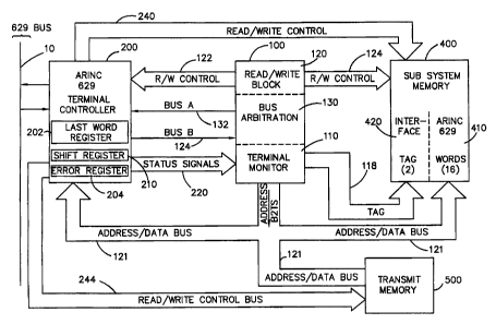
Shown in Figure 1 is a block diagram of the memory interface system 100 of the
present invention in combination with an ARINC 629 terminal controller 200
including
last word register 202 and error register 204, an ARINC 629 bus 10, and
subsystem
memory 400.
Terminal controller 200 serves to receive data message transmitted on the bus
10, and transmit data messages stored in transmit memory 500 in accordance
with the
ARINC 629 Standard as published by in Boeing document, CAGE CODE 8120,
CONTROLLED BY ARINC 629 DATA BUS (B-E82U), document D227W I 02,
ARINC 629 TERMINAL CONTROLLER UNIVERSAL DATA SHEET, Revision
C, Master Dated 4/20193. The aforementioned document describes the physical
and
t 5 electrical characteristics of the Terminal Controller, regardless of the
manufacturer. The
AC and DC electrical characteristics contained therein are the worst case
values for all
the suppliers. This document has been created to remove the need of the
designer to
consult all the suppliers data sheets to determine the AC and DC
characteristics envelop.
ARINC 629 is a multiple transmitter, broadcast-type, autonomous terminal
2o access, time-division multiplex system that supports quasi-real time data
communication
between many terminals over a common single-channel transmission medium. One
ARINC 629 Terminal Controller with its accessory components forms a two-way
interface between the single channel (serial) medium and one or several
(parallel) data
ports of local subsystems.
25 The Terminal Controller is a VLSI device contained in a 180-pin pin grid
array
package. It provides an interface to and from a global ARINC 629 serial data
bus and a
parallel 16-bit wide subsystem bus. Typically the Terminal Controller is
connected to
the serial medium by means of line driverlreceiver components, gets access
protocol
parameters from groundstcaps, and task-specific parameters from PROMS. The
3o subsystem interface takes the form most suitable for the specific
application in question.
In its primary mode, the Terminal Controller operates as a digital autonomous
access controllerltransceiver. Transmission is enabled through a series of
access timers,
CA 02129157 2004-05-12
64159-1349
two of which have global values, and the third is specific for each Terminal
Controller
on the serial data bus. Data is sent on the bus using Manchester II Biphase
coding at
two megabit per second (Mps). A label word precedes each string of data words
to
identify the data. The receiver functions both as a transmission monitor and
global bus
receiver. In the monitor mode, the receiver prevents the Terminal Controller
from
transmitting outside of its unique access time slot. The receiver function
monitors the
bus at all times when the Terminal Controller is not transmitting, listening
for a match
with parameters stored in its Receive Personality PROM (RPP). The receiver
decodes
each incoming label and determines if the information following it is required
by the
1o attached user(s). If a match is detected, the serial data is captured and
sent to the
subsystem for data storage.
The terminal controller 200 includes the last word monitor, or simply the last
word internal register 202. The last word register 202 contains the last label
or data
word sent for a transmit operation, or the last label word received for a
receive
operation, but does not store received data words from the received data
message during
the receive operation: The last word register 202 allows for wrap-around
verification of
transmitted data and recovery of the label word from received data.
It should be noted that terminal controller 200 includes a non-accessible
serial to
parallel shi$ register 210 for placing the received data words autonomously on
the
2o addressldata buss and control an external memory by read write control
lines 240, and
autonomously accesses the transmit memory data on address/data bus 121 through
read/write control bus 244 connected to transmit memory 500.
The terminal controller 200 further includes an Interrupt Vector Register
(IVR)
which contains the fifteen bit interrupt vector for the current received or
transmitted
word string. The most significant bit of the IVR contains the string error
bit. The IVR
makes available to a subsystem the value of the current interrupt vector at
any time
whether or not the personality proms (RPP or XPP) have been programmed to
provide
interrupt vector strobes.
The terminal controller 200 also includes the Error Register 204 which
contains
3o not only error information but other diagnostic information as well. All
but four of the
sixteen bits conform to a "latch and hold" arrangement in which errors are
latched as
they occur and held until the Error Register is read. Following a read, these
errors are
CA 02129157 2004-05-12
64159-1349
-5-
zeroed. The "latch and hold" error information cannot change while the error
register is
being read. Any errors that occur following DSO being asserted will be
reflected in the
next error register access. It should be noted that these twelve "latch and
hold" bits
provide an error history rather than transient error status. The additional
four bits are
not latched and reflect the current status of the Terminal Controller.
In accordance with the present invention, subsystem memory 400 is a FIFO
(first-in, first-out) 18 bit memory device. The 18 bit FIFO memory device 400
is
allocated such each memory byte has 16 data bits dedicated for the ARINC 629
data
output bus lines, indicated by numeral designation 410, and 2 bits dedicated
as tag bits,
1o indicated by numeral designation 420.
The function of memory interface system 100 is to read the last word register
202 of the terminal controller 200 for storing label words and data words,
including
transmitted data words into the subsystem memory 400, and also reading the
error
register 204 of the terminal controller for storing the error register word in
the
subsystem memory 400. Further, memory interface system 100 appends tag bits to
all
words written into the subsystem memory 400. to identify them as label words,
data
words, or error words. The memory interface system 100 cooperates with
input/output
control signals of the terminal controller 200 and subsystem memory 400 for
arbitrating
the address/data bus connected therebetween.
2o Memory interface system 100 includes three functional blocks as depicted by
the
terminal monitor block 110, the read/write control block 120, and the bus
arbitration
block 130. Terminal monitor block 110 provides signal monitoring of terminal
controller status signals 230, read/write control block 120 provides
readlwrite control
signals 122 for controlling terminal controller 200, and readlwrite control
signals 124
for controlling subsystem memory 400.
The terminal monitor block 110 receives outputs from the terminal controller
200 to perform three functions. The first is to determine when the terminal
controller
200 contains data desired by the subsystem. ~ If necessary the address/data
bus 121 will
be requested so that the read/write block 120 may facilitate reading the last
word
3o register 202 and transfer the data to the subsystem memory 400. The second
function of
the terminal monitor block 110 is to determine the appropriate tag that is to
be appended
to words written into the subsystem memory 400. The last function is to set
the address
CA 02129157 2004-05-12
64159-1349
-6-
of the appropriate terminal controller 200 registers, i.e., last word register
202 and error
register 204; to be read by the read/write block.
The bus arbitration block 130 grants temporary control of the address/data bus
121 to the terminal controller 200 or the memory interface system 100, and
prevents
contention therebetween. The Bus arbitration block 130 responds to requests
for the bu.s
120 received from the terminal controller 200 and the terminal monitor block
110 of the
terminal monitor block 110. Both must request the bus for each bus cycle
required.
Each bus request must be removed before the next request is granted. When the
terminal monitor block 110 request the bus, the bus arbitration block sends an
to acknowledge to the read/write block 120 to begin a cycle.
The read/write block 120 receives an acknowledge from the bus arbitration
block
130 to begin a read/write cycle. Then label words, wrap-around data words, and
error
register contents may be strobed out of the last word register 210 of terminal
controller
200, and written into the subsystem memory 400 with the appropriate tag
appended
thereto.
' The following is general list of signals and their description which may be;
employed in one form or another for practicing the invention:
STATUS SIGNAL INPUTS, Inputs
C8MHZ The C8MHZ input is an 8 MHz clock used to clock the EPLD. It
is synchronous to the TC clocks.
STAC The STAC input from the TC is used by the terminal monitor
block to indicate that data (including wrap-around data) is being
received or that the Error Register should be read. This signal is
also used to determine tag bits and internal register address bits.
(active low)
3o The string active signal, STAC, is low for the duration of the
Terminal Controller/subsystem bus activity in a word string for
both receive and transmit operations. Again, the exception to this
2129157
rule is that STAC will also go low for a label-only word string. It
goes low just after a leading interrupt vector strobe and high just
after a trailing interrupt vector strobe. Therefore, it can be used to
distinguish between leading and trailing interrupts. STAC always
goes low at the same time relative to the transmitlreceive word,
but is reset depending upon the end of the DMA sequence. All
timing diagrams were drawn to show latest STAC reset. The
timing relationship of STAC to the transmitted/received word
string is detailed in Figures ~~ and 3b.
This signal can also be used to prevent data slicing of the
transmittedlreceived word string by the host. When low, the
signal indicates to the host that the data in memory is being
transmitted or received. The preserve string coherency, STAC
would be used to prevent the host from reading or writing the
data block until the transmission/reception is completed.
RIVS The RIVS input from the TC is used by the terminal monitor
block to indicate that data is being received. This signal is also
2o used to determine tag bits and internal register address bits.
(active low)
This is a low active pulse that indicates to the host that the receive
interrupt vector is valid on the AOF-O lines. The relationship
z5 between the received word string and the leading and trailing
interrupt vector strobes is illustrated in Figure 3a .
XIVS The XIVS input from the TC is used by the terminal block
monitor to indicate that wrap-around data is being received. This
3o signal is also used to determine tag bits and internal register
address bits. (active low)
2129151
_g_
This is a low active pulse that indicates to the host that the
transmit interrupt vector is valid on the AOF-0 lines. The
relationship between the transmitted word string and the leading
and trailing interrupt vector strobes is illustrated in Figure 3b .
BUSQ The BUSQ input from the TC is used by the terminal monitor to
indicate that a word will be available in the Last Word Monitor
Register. (active high)
to This is a test/diagnostic signal that is defined as going active high
when the Terminal Controller does not detect any activity on the
Global ARINC 629 bus. In addition, the BUSQ goes high when
the Terminal Controller detects a valid word in its decoder.
BUSQ can be used to indicate when the internal registers contain
t5 valid data, as detailed in the timing diagrams Fige. 3a and 3b.
WAIT The WAIT input from the TC is used by the terminal monitor
block to extend the duration of the read cycle when reading the
Last Word Monitor Register. (active low)
RWO The RWO input from the TC is used by the read/write block to
strobe receive data into the RX FIFOs. (read high/write low)
DSI The DSI (DSO) input from the TC is used by the read/write block
to strobe receive data into the RX FIFOs. (active low)
BUSR The BUSR input from the TC is used by the bus arbitration block
to grant bus control to the TC. (active low)
3o RX RST The RX_RST input is used to reset and initialize the LWM
EPLD. (active low)
2129157
-9-
PAL 1 RST The PAL 1 RST input is used to reset and initialize the L WM
EPLD from external test equipment. (active low)
RESET _The RESET output generated by the terminal monitor block is
used to initialize the LWM EPLD. (active high)
RX-IN-PROG The RX_IN_PROG output generated by the terminal monitor
l0 indicates that data is being received and is used to determine tag
bits and internal register address bits. (active high)
TX IN_PROG The TX IN-PROG output generated by the terminal monitor
block indicates that Wrap-around data is being received and is
1 s used to determine tag bits and internal register address bits.
(active high)
RX REQ The RX REQ output generated by the terminal monitor block is
used to generate requests for the address/data bus to read labels
2o and error registers for receive data. (active high)
TX REQ The TX REQ output generated by the terminal monitor block is
used to generate requests for the address/data bus to read labels
and wrap-around data for transmitted data. (active high)
T'X_REQ RST The TX REQ_RST output generated by the terminal monitor
block is used to reset the TX REQ output after words have been
read from the internal registers of the TC. (active high)
3o TX REQ DLY The TX REQ DLY output generated by the terminal monitor
block is the TX REQ output delayed by a 1 microsecond to be
sure data is valid in the internal registers of the TC. This output
2129157
-lo-
is used to generate requests for the address/data bus to read labels
and wrap-around data for transmitted data. (active high)
DIV2 The DIV2 output generated by the terminal monitor block is used
to delay the TX-REQ output. When enabled by TX-REQ the
_DIV2 output divides the BMHz by 2.
DIV4 The DIV4 output generated by the terminal monitor block is used
to delay the TX REQ output. The DIV4 output dives the DIV2
output by 2.
DIV8 The DIV8 output generated by the terminal monitor block is used
to delay the TX REQ output. The DIV8 output dives the DIV4
output by 2.
TX ER REQ The 'TX_ER REQ output generated by the terminal monitor
block is used to generate requests for the address/data bus to read
the error register after transmitted data has been written to the RX
FIFOs.. (active high)
TX ER RST The T'X_ER RST output generated by the terminal monitor block
is used to reset the TX ER REQ output after the error register
has been read. {active high)
TER DATA The TER DATA output generated by the terminal monitor block
is used to enable the request to read the error register. (active
high)
RD_REQ The RD_REQ output generated by the terminal monitor block is
3o used to generate requests for the address/data bus to read labels,
wrap-around data, and the error register for transmitted data.
(active high)
2129157
AD17 The AD17 output generated by the terminal monitor block is one
of two tag bits used to identify words written into the RX FIFOs
as label, data or error register. ( 11 = label, O l = data, 00 = error
register)
AD 16 The AD 16 output generated by the terminal monitor block is one
of two tag bits used to identify words written into the RX FIFOs
as label, data or error register. (11 = label, O1 = data, 00 = error
to register)
AD 1 The AD 1 tristate output generated by the terminal monitor block
is one of two address bits used to select the last word monitor
register or the error register when reading data from the TC. (Ol =
last word monitor register, 00 = error register)
ADO The ADO tristate output generated by the terminal monitor block
is one of two address bits used to select the last word monitor
register or the error register when reading data from the TC. (O1 =
last word monitor register, 00 = error register)
ADO EN The ADO EN output generated by the terminal monitor block is
used to enable the tristate drivers for the AD 1 and ADO outputs
when raiding data from the TC. (active high)
L BUSR The L BUSR output generated by the bus arbitration block is
used to determine when control of the address/data bus is to be
granted to the TC. (active high)
3o BUSA The BUSA output generated by the bus arbitration clock is used
to grant control of the address/data bus to the TC. (active low)
2129157
-12-
RD_OUT The RI7_OUT output generated by the bus arbitration block is
used to grant control of the address/data bus to read/write block
of the L WM. (active high)
RD_OUT RST _ The RD_OUT RST output generated by the bus arbitration block
is used to reset the RD OUT output when control has been given
to the TC.
CS The CS output generated by the read/write block is used to enable
access to the internal registers of the TC. (active low)
DLY ASO The DLY ASO output generated by the read/write block is used
to set up the ASO output during accesses to the internal registers
of the TC. (active high)
ASO The ASO output generated by the read/write block is used to
validate address during accesses to the internal registers of the
TC. (active low)
2o DLY DSO The DLY DSO output generated by the read/write block is used
to set up the DSO output during accesses to the internal registers
of the TC. (active high)
DSO The DSO output generated by the read/write block is used to
strobe data out of the internal registers of the TC. (active low)
WR1 The WR1 output generated by the read/write block is used to
strobe internal register data (labels, wrap-around data, and error
register) and tag bits into the RX FIFOs. (active low)
WR FIFO The WR_FIFO output generated by the read/write block is used
to strobe receive data and tag bits into the RX FIFOs. (active low)
CA 02129157 2004-05-12
64159-1349
-13-
CLR ER The CLR ER output generated by the read/write block is used to
clear the TX ER REQ output after the error register has been
read. (active high)
CLR READ The CLR READ output generated by the read/write block is used
to clear the terminal monitor block after an internal register has
been read. (active high)
1o Illustrated in Figure 2 is a block diagram similar to Figure 1 showing more
particularly some of the aforementioned signal lines. Illustrated in Figures
3a and 3b are
timing directing illustrating the relationship of the terminal controller 200
status signals
during receive mode and transmit mode, respectively.
Referring again to Figure 1, transmit memory 500 is also coupled to
address/data
bus 121 aad may be controlled by terminal controller 200 through read/write
control
lines bus 244; and similarly subsystem memory may be controlled by terminal
controller
200 through read/write control lines bus 240.
The general operation of the memory interface system 100 will now be
described. During the receive mode, the first data word received is the label
word, and,
2o is stored in the last word register 202. The terminal controller 200 puts
out status
signals 220 to initiate action by the memory interface system 100 to cause the
contents
of the last word register 202 to be placed on the addressJdata bus 121. At the
same time,
the tag bits are set such that when a writ command is given by read/write
block 120, the
label word and label tag are stored in subsystem memory 400.
Continuing, the status signals will then dictate transfer of control to the
terminal
controller 200 to autonomously write data words into subsystem memory 400
through
use of read/write control buss signal from terminal controller 200 to
subsystem memory
400. However, before allowing this action to take place, the tag bits are set
to indicate
that words written in memory are data words of the received message.
3o When the status signals again indicate that the data message is complete,
control
is transferred back to the memory interface system 100, which in turn causes
the error
register to be read, transferred to the' memory, and tag bits set and stored
therewith.
CA 02129157 2004-05-12
64159-1349
-14-
In the transmit mode of terminal controller 200, terminal controller 200
autonomously addresses transmit memory 500 and allows the words therein to 'be
transferred to the address/data bus 121 as inputs
to terminal controller 200 for subsequent
transmission to ARINC 629 bus. However, in this transmit mode all of the words
are
temporally stored in the last word register. Accordingly, memory interface
system 100
acknowledges this situation and causes the last word register transferred to
subsystem
memory 400 along with the appropriate tag bits, including both the transmitted
label
word, as well as a reading of the error register including tag bits after the
data message
has been completed. This is the so called wrap-around mode for subsequent data
to comparison of that which was transmitted and which was stored, thereby
providing a
means for detection of any faults in the system.
In practice of the present invention, the memory interface system 100
including
allof it functional blocks may be constructed by employment of an Erasable
Programmable Logic Device, for example an ALTERA EP1810, or by a wide array of
electrical circuit components to achieve the intended function of the memory
interface
system 100.
Figures 4, 5, and 6 illustrate schematic circuit diagrams of the configuration
of
the Erasable Programmable Logic Device for achieving the terminal monitor
block 110,
the read/write block 120, and the bus arbitration block 130, respectively.
2o It should be recognized by those skilled in the art that circuit
construction
beyond that which has been disclosed herein is intended to be within the true
spirit and
scope of the present invention. Although a specific embodiment has been shown
for
multi-channel data receiver system in accordance with present invention,
others are of
course possible within the level of skill in the art, and are within the true
spirit and
scope of the present invention.
More specifically, the foregoing description has been set forth in terms of
functional block diagrams including registers, counters, timers, and logic
means, and
also illustrated in terms of flow diagrams to enhance understanding of the
present
invention without burdening the reader with detail well known within the level
of those
skilled in the art. There are, of course, a wide array of implementations for
achieving
the intended function as depicted in the accompanying claims, all of which are
intended
to be within the true spirit and scope of the present invention It should also
be noted
2129157
-ls-
that although a specific embodiment has been illustrating specific memory
devices,
there are of course a wide array of components for serving the intended
function. More
specifically, FIFO memories may be implemented by an addressable random access
memory. Lastly, although the embodiment of the invention has been illustrated,
at least
in part, by specific data transfer being serial or parallel, alternate
arrangements are, of
course, within the true spirit of the present invention is defined by the
accompanying
claims.
It should also be noted that all, or selected ones of any of the electrical
circuit
components may be configured into a single integrated circuit and that the
separation of
to components as illustrated ion the Figures is within the true spirit of the
present invention
is defined by the accompanying claims.