Note: Descriptions are shown in the official language in which they were submitted.
~-ro~ u
2~L2~7~7
METHOD AND APPARATUS FOR REDUCING ME~vIORY
REQUIREMENTS IN A REDUCED LI~E, ACTIVE ADDRESSING
DISPLAY SYSTEM
Field of the Invention
This invention relates in general to addressing methods for
addressing displays, and more specifically to a method and apparatus for
reducing memory requirements in active-addressed displays.
'
13ackground of the Invention
An example of a direct multiplexed, rms (root mean square~
responding electronic display is the well-known liquid crystal display
15 (LCD). In such a display, a nematic liquid crystal material is positioned
between two parallel glass plates having electrodes applied to eac~ surface -
in contact with the liquid crystal material. The electrodes typically are
arranged in vertical columns on one plate and horizontal rows on the
other plate for driving a pichlre element (pixel) wherever a column and ~ ~row electrode overlap. ~ ~ -
In rms-responding displays, the optical state of a pixel is substantially
responsive to the square of the voltage applied to the pixelt i.e., the
difference in the voltages applied to the electrodes on the opposite sides of
the pixel. LCl:)s have an inherent time constant that characterizes the time
required for the optical state of a pixel to retum to an equilib~iunn state
after the optical state has been modi~ied by changing the voltage applied to -
the pixel. Recent technological advances have produced LCDs with time ;-
constants (approximately 16.7 milliseconds) approaching the frame period
used in many video displays. Such a short time constant allows the LCD
to respond quickly and is especially advantageous for depicting motion
without noticeable srnearing or flickering of the displayed image.
Conventional direct multiplexed addressing methods for LCDs
encounter a problem when the display time constant approaches the
frame period. The problem occurs because conventional direct
multiplexed addressing methods subject each pixel to a short duration
"selection" pulse once per frame. The voltage level of the selection pulse
is typically 7-13 times higher than the rms voltages averaged o-~er the
~rolox~!
~Z~7~7
frame period. The optical state of a pixel in an LCD having a short time
constant tencls to return towards an equilibrium state between selection
pulses, resulting in lowered image contrast, because the human eye
integrates the resultant brightness transients at a perceived intermediate
level. In addition, the high level of the selection pulse can cause .
alignment instabilities in some types of LCDs.
To overcome the above-described problems, an "active addressing"
method for driving rms responding electronic displays has been
developed. The active addressing method continuously drives tlhe row
electrodes with signals comprising a train of periodic pulses having a
common period T corresponding to the frame period. The row signals are
independent of the image to be displayed and preferably are orthogonal
and normalized, i.e., orthonorrnal. The term "orthogonal" denotes that, if
the amplitude of a signal applied to one of the rows is multiplied by the
amplitude of a signal applied to another one of the rows, the integral of
this product over the frame period is zero. The term "normalize~"
denotes that all the row signals have the same rms voltage integrated over
the frame period T.
During each frame period a plurality of signals for the colu~
electrodes are calculated and generated from the collective state of the
pixels in each of the columns. The column voltage at any time t during
the frame period is proportional to the sum obtained by considenng each
pixel in the column, multiplying a "pixel value" representing the optical
state (either -1 for fully "on", +1 for fully "off", or values between -1 and
+1 for proportionally corresponding gray shades) of the pixel by the value
of that pixel's row signal at time t, and adding the products obtained
thereby to the sum. In effect, the column voltages can be derived by
transforming each column of a matrix of incoming image data b~- the
orthonormal signals utilized for driving the rows of the display.
If driven in the active addressing manner described above, it can be
shown mathematically that there is applied to each pixel of the d~splay an
rms voltage averaged over the frame period, and that the rms voltage is
proportional to the pixel value for the frame. The advantage of active
addressing is that it restores high contrast to the displayed image because,
instead of applying a single, high level selection pulse to each pixel during
the frame period, active addressing applies a plurality of much lower level
(2-5 times the rms voltage) selection pulses spread throughout the ~rame
1''1'~1()~0~
;~2976~
period In addition, the much lower level of the selection pulses
substantially reduces the probability of alignment instabilities. As a result,
utilizing an active addressing method, rms responding electronic displays,
such as LCDs utilized in portable radio devices, can display image data at
5 video speeds without smearing or flickering. Additionally, LCDs driven
with an active addressing method can display image data having multiple
shades without the contrast problems present in LCDs driven with
conventional multiplexed addressing methods.
A drawback to utilizing active addressing results from the large
10 number of calculations required to generate column and row signals for
driving an rms-responding display and the large amount of memory ~ -
required for storage of thie signals. For example, a display having 480 rows
and 640 columns requires approximately 230, 400 (# rows2) operations
simply for generation of the column values for a single column during
15 one frame period. While it is, of course, possible to perform calculations
at this rate, such complex, rapidly performed calculations necessitate a
large amount of power consumption. Thierefore, a method referred to as
"reduced line addressing" has been developed.
In reduced line addressing, the rows of a display are evenly divided
20 and addressed separately. If, for instance, a display having 480 rows and
640 columns is util~zed to display image data, the display could be divided
into eight groups of sixty (60) rows, which are each addressed for 1/8 of the
frame time, thus requiring only 60 (rather than 480) orthonormal signals
for driving the rows. In operation, columns of an orthonormal matrix,
25 which is representative of the orthonormal signals, are applied to rows of
the different segments during different time periods. During the different
time periods, the columns of the display are driven with rows of a
"transformed image diata matrix", which is representative of the image
data which has been previously transformed, as described above, utilizing
30 the orthonormal signals. In reduced line addressing, however, the
transformed image data matrix can be transformed using the smaller set of
orthonorrnal signals, i.e., using 60 orthonormal signals rather than 480
orthonormal signals. More specifically, the image data matrix is divided
into segments of 60 rows, and each segment is transformed in an
35 independent transformation using the 60 orthonormal signals to generate
L.he transformed image data matrix.
1' 1'() 1()~
-' 2~297~i7
Using the reduced line addressing method as described,
approximately 3,600, i.e., 60Z operations are required for generation of the
column voltages for a single column during each segment time. Because
the frame period has been divided into eight segments, the total nurnber
of operations for generation of the column voltages for a single column
during the frame period is approximately 28, 800, i.e., 8 ~ 3,600. Therefore,
in the above-described example, generating column values for drivinO a
single column of a 480 x 640 display over an entire frame period using
reduced line addressing requires only an eighth of the operations
necessary for column voltage generation when the clisplay is addressed as
a whole. It will be appreciated that the reduced line addressing rnethod
~erefore necessitates less power and less time for performance of the
required operations.
However, because the signals for driving the rows and columns of
the display are distributed in time when reduced line addressing is used,
all of the column signals for driving the columns of the display over an
entire frame period must be derived and stored in memory prior to
driving the display. Therefore, depending upon the size of the display, the
amount of memory required for storage of the signals can be quite large,
and the memory requirements are not reduced from the requirements of
conventional active addressing techniques. In fact, in some chips
currently used for driving displays using active addressing techniques, the
memory required for calculation and storage of the column signals can
consume up to 90~/O of the chip.
Thus, what is needed is method and apparatus for reducing the
amount of memory required for derivation and storage of column signals
for driving columns of an active-adclressed display.
Summary of the Invention
A method for driving a display, rows of which are divided into at
least first and second segments, comprises the step of driving, during a
first plurality of sequential time slots, a first plurality of rows included in
the first seO~nent with first voltages associated with a first subset of
functions included in a complete set of orthonormal functions. The
method further comprises the step of driving, during the first plurali~y of
sequential time slots, a second plurality of rows included in the second
_ ~ . ' ' . ' : , ' . ' , ', '' .
0~ Z~297~ ~
segment with second voltages associated with a remaining function : ~
included in the complete set of orthonormal functions, wherein the ~ -
remaining function is not included in the first subset of functions.
A data communication receiver receives and stores a set of irnage ~
data and displays images associated therewith on a display having rows ~ ~ -
divided into first and second segments. The data communication receiver
comprises a database for storing a set of orthonormal functions and row ~ -
drivers coupled to the database for driving the first segment of the display -~
with first voltages associated with a first subset of orthonormal functions
and driving the second segment of the display with second voltages
associated with a remaining hmction included in the set of or~onormal
functions during a first plurality of sequential time slots. The row dri~ers
also drive the first segment with the second voltages associated with the
remaining function and drive the second segment with the first YoltageS
associated with the first subset of orthonormal functions during a second
plurality of sequential time slots.
Brief Description of the Drawings
FIC:;. 1 is a front orthographic view of a portion of a conventional
liquid crystal display.
FIG. 2 is an orthographic cross-section view along the line 2-2 of
FIG. 1 of the portion of the conventional liquid crystal display.
FIG. 3 is a matrix of Walsh functions in accordance with the present
invention.
FIG. 4 depicts drive signals corresponding to the Walsh functions of
FIG. 3 in accordance with the present invention.
FIG. 5 is a front orthographic view of a conventional liquid cnrstal
display which is divided into segments that are addressed in accordance
with conventional reduced line addressing techniques.
FIG. 6 is an electrical block diagram of an electronic device
comprising a liquid cr,vstal display which is addressed in accordance with
the present invention.
E~IG. 7 depicts column matrices associated with column voltages and
row matrices associated with row voltages for driving a liquid crystal
display having two segments which are addressed in accordance with the -
present invention.
1~ r()lo~o~ 21Z9767
FIG. 8 depicts row matrices associated with row voltages ~or driving
a liquid crystal display having y number of segments, each including x
number of rows addressed in accordance with the present invention.
FIG. 9 depicts column matrices associated with column voltages for
5 driving coluIru~s of a liquid crystal display in accordance with the present
invention.
FI~:s. 10-12 are flowcharts illustrating the operation of a controller
included in the electronic device of FIG. 6 when driving a liquid crystal
display, the rows of which are divided into segments, in accordance with
10 the present invention.
Description of a Preferred Embodiment
Referring to FI(:~s. 1 and 2, orthographic front and cross-section
15 views of a portion of a conventional liquid crystal display (LCD) 100 depict
first and second transparent substrates 102, ~06 having a space
therebetween filled with a layer of liquid crystal material 202. A perimeter
seal 204 prevents the liquid crystal material from escaping from the LCD
100. The LCD 100 further includes a plurality of transparent electrodes
20 comprising row electrodes 106 positioned on the second transparent
substrate 206 and column electrodes 104 positioned on the first transparent
substrate 102. At each point at which a column electrode 104 overlaps a
row electrode 106, such as the overlap 108, voltages applied to the
overlapping electrodes 104,106 can control the optical state of the liquid
25 crystal material 202 therebetween, thus forming a controllable picture
element, hereafter referred to as a "pixel". While an LCD is the preferred
display element in accordance with the preferred embodiment of the
present invention, it will be appreciated that other types of display
elements may be used as well, provided that such other types of display
30 elements exhibit optical characteristics responsive to the square of the
voltage applied to each pixel, similar to the root mean square (rms~
response of an LCD.
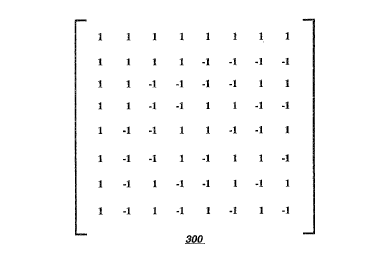
Referring to FIGs. 3 and 4, an eight-by-eight (third order) matrix of
Walsh functions 30Q and the corresponding Walsh waves 400 in
35 ~ccordance with the preferred embodiment of the present invention are
shown. Walsh functions are both orthogonal and normalized, i.e.,
orthonormal, and are therefore preferable for use in an active-addressed
, '.,,' j ' ,. ' ~ , ~, :' ', :'' i ' ' , , , " ", ' ' ' ' ' ' '
~r~lo~
2~L29~67
display system, as briefly d;scussed in the Background of the Invention
herein above. It may be appreciated by one of ordinary skill in the art that
other classes of functions, such as Pseudo Random Binary Sequence
(PRBS~ functions or Discrete Cosine Transform (DCT) functions, may also
5 be utilized in active-addressed display systems.
When Walsh functions are used in an active-addressed display
system, voltages having levels represented by the Walsh waves 400 are
uniquely applied to a selected plurality of electrodes of the LCD 100. For
example, the Walsh waves 404, 406, and 408 could be applied to the first
10 (uppermost), second and third row electrodes 106, respectively, and so on.
In this manner, each of the Walsh waves 400 would be applied uniquely to
a corresponding one of the row electrodes 106. It is preferable not to use
the Walsh wave 402 in an LCD application because the Walsh wave 402
would bias the LCD 100 with an undesirable DC voltage.
It is of interest to note that the values of the Walsh waves 400 are
constant during each time slot t. The duration of the time slot t for the
eight Walsh waves 400 is one-eighth of the duration of one complete cycle
of Walsh waves 400 from start 410 to finish 412. When using Walsh
waves for actively addressing a disp]ay, the duration of one complete cycle
20 of the Walsh waves 400 is set equal to the frame duration, i.e., the time to
receive one complete set of data for controlling all the pixels 108 of the -
LCV 100. The eight Walsh waves 400 are capable of uniquely driving up to -
eight row electrodes 106 (seven if the Walsh wave ~02 is not used). It will
be appreciated that a practical display has many more rows. For example,
25 displays having four-hundred-eighty (480) rows and six-hundred-forty
~640) columns are widely used today in laptop corIlputers. Because Walsh
function matrices are available in complete sets determined by powers of
two, and because the orthonormality requirement for active addressing
does not allow more than one electrode to be driven from each Walsh
30 wave, a five-hundred-twelve by five-hundred-twelve (29 x 24) Walsh
function matrix would be required to drive a display having four- -
hundred-eighty row electrodes 106. For this case, the duration of the time
slot t is 1/512 of the frame duration. Four-hundred-eighty Walsh waves
would be used to drive the four-hundred-eighty row electrodes 106, while
35 the rernaining thirty-two, preferably including the first Walsh wave 402
having a Ds~ bias, would be unused.
r(~lo~
~129~7~7
The columns of the LCD 100 are, ~t the same time, dri~en with
column voltages derived by transforrning the image data, which can be
represented by a matrix of image data values, utilizing orthonormal
functions representative of the Walsh waves 400. This transformation can
5 be accomplished, for example, by using matrix multiplication, Walsh
Transforms, modifications of Fourier Transforms, or other such
algorithms. In accordance with active addressing methods, the rms
voltage applied to each of the pixels of the LCD 100 during a frame
duration approximates an ;nverse transformation of the column voltages,
10 thereby reproducing the image data on the LCD 100.
Referring next to FIG. 5, an illustration depicts a conventional
active-addressed LCD, such as the LCD 100, which is driven in accordance
with reduced line addressing techniques, thereby reducing the power
necessary for driving the LCD 100, as described briefly hereinabove in the
15 Background of the Invention. As shown, the LCD 100 is divided into
segments, each of which comprises an equal number of rows. For
illustrative purposes only, the LCD 100 is depicted as having only eight
columns and eight rows, which are evenly divided into two segments ~0,
502 of four rows each. The two segments 500, 502 are addressed separately
20 using matrices of orthonormal functions, such as Walsh functions.
Because each segment 500, 502 comprises only four rows, the matrix 50
used for driving each segment 500, 502 need only include four
orthonormal functions having four values each. Additionally, the
orthonormal matrix 504 is used for transforming the image data, which is
25 preferably in the form of an image data matrix. For the current example,
in which an eight-by-eight LCD 100 is divided into two segments 500, ~02,
the orthonormal function matrix 504 is used first to transform the first
four rows of the image data matrix, and then to transform the second fcur
rows of the image data, thereby generating an entire transformed image
30 data matrix 506, which includes column values for driving columns of the
LCD 100 during the frame duration.
In operation, row drivers (not shown) are employed to drive,
during a first time period, the first four rows of the LCD 100 with row
voltages associated with the values in the first column of the orthonormal
35 matrix 504. For instance, during the ffrst time period, row 1 is driven with
voltage a1, row 2 is driven with voltage a2, row 3 is driven with voltag,e n3
and row 4 is driven with voltage a4. At the same time, the columns are
,: , -, ; ,~ .~ . ~ .................. .. ..
,. ; . . . . . .... . .
l~TO l ~
2~2~767
driven with voltages associated with values included in the first row of
the transformed image data matrix 506. During the second time period,
the second four rows of the LCD 100 are driven with row voltages
associated with the values in the first column of the orthonormal matrix
5 504. Specifically, row 5 is driven with voltage al, row 6 is driven with
voltage a2, row 7 is driven with voltage a3, and row 8 is driven with
voltage a4. At the same time, the columns of the LCD 100 are driven with
voltages associated with values included in the fifth row of the
transformed image data matrix 506, as shown. During the third time
10 period, the first four rows of the LCD lG0 are again driven, this time with
row voltages associated with the values in the second colwrLn of the
orthonormal matrix 504. Simultaneously, the columns are driven with
voltages associated with values included in the second row of the '
transforrned image data matrix 506. This operation continues until, after
15 eight time periods, the rows of each of the segments have been addressed
with all of the columns of the orthonormal matrix 504, and the columns
of the LCD 100 have been addressed with all of the rows of the
transformed image data matrix 506. -~
In reduced line addressing, the number of operations necessary for
driving the columns of a display is greatly reduced when compared to the
number necessary when an entire display is addressed as a whole.
Therefore, reduced line addressing requires less power consumption than
conventional active addressing. However, the memory requirements for
reduced line addressing are quite large because all of the column signals,
i.e., the entire transformed image data matrix 506, must be derived and
stored prior to addressing the LCD 100. For a small display, the storage of
all of ~he column signals may not consume too much space, but, for larger
displays, the storage of the column signals can easily consume up to 90%
of a chip which generates the column signals. As a result, an electronic
device utilizing a display which is driven using conventional reduced line
addressing techniques must be large enough to accommodate not only
sufficient memory for storage of operating parameters and subroutines,
but also all of the column signals for addressirlg the entire display during
an entire frame duration.
FIG. 6 is an electrical block diagram of an electronic device which
receives and displays image data on an LCD 600, the rows of which are
divided into segments such that the LCD 600 can be addressed in
1 0~ 0 ~'
--- 21297~i7
accordance with the present invention, thereby sa- ing memory and power
necessary for computation and storage of column values. When the
electronic device is a radio communication device 605, as shown, the
image data to be displayed on the LCD 600 is included in a radio frequency
5 signal, which is received and demodulated by a receiver 608 internal to the
radio communication device 605. A decoder 610 coupled to the receiver
608 decodes the radio frequency signal to recover the image data therefrom
in a conventional manner, and a controller 615 coupled to the decoder 610
further processes the image data.
Coupled to the controller 615 is timing circuitry 620 for establishing
system timing. The ~iming circuitry 620 can, for example, comprise a
crystal ~not shown) and conventional oscillator circuitry (not shown).
Additionally, a memory, such as a read only memory (ROM) 625, stores
system parameters and system subroutines which are executed by the
15 controller 615. The system parameters can include, for example, the
number y of segments into which the LCD 600 is divided~ the number x of
rows included in each segment, and z, the nearest power of two greater
than x. The subroutines can include, for example, a column matrix
subroutine perforrned to generate column values for addressing columns
20 of the LCD 600 and an addressing subroutine performed to address both
the columns and the rows of the LCD 600. A random access memory
(RAM) 630, also coupled to the controller 615, is employed to store the
incoming image data as an image data matrix and to temporarily store
other variables, such as the generated column values in the form of a
25 column matrix for each segment, derived during operation of the radio
communication device 605. Additionally, counters 632, 634 coupled to the
controller 615 store counter values which are incremented during the
addressing of the LCD 600.
Preferably, the radio communication de~,-ice 605 further comprises
30 an orthono~mal matrix database 635 for storing a set of orthonormal
functions in the form of a matrix. The orthononnal functions can be, as
described above, Walsh functions, DCT functions, or PRBS functions, the
number of which must be greater than the number of rows incIuded in
each segment of the LCD 600. In accordance with the present invention,
35 the number of rows included m each segment of the LCD 600 is not equal
to a power of two, thereby ensuring that, when Walsh functions are
utilized, the number of Walsh functions is greater than the number of
~-r()~ ou
Z~29767
11 :
rows included in each segment because Walsh function matrices are
available in complete sets determined by powers of two.
Preferably, the set of orthonormal functions are separated into a set -~
of "used" functions, stored in the form of a "used function" matrix for
5 addressing some segments of the LCD 600, and a remaining, or leftover,
function for addressing other segments of the LCD 600, as will be described
in detail below. The used function matrix preferably includes a number of
orthonormal functions equal to the number x of rows per segment, and
the remaining orthonormal function is a leftover orthonormal function
10 not included in the used function matnx. In accordance with the
preferred embodiment of the present invention, coefficients of the
remaining function are divided by a scaling factor p, which is determined
by the number of rows in the LCD 600 and the number of segments into
which the LCD 600 is divided. Alternatively, rather than scaling the
15 remaining function before storage in the database 635, the remaining
function could be stored in an unscaled form, then simply scaled by the
controller 615 before use. However, because it is not anticipated that the
size of the LCD 600 or the number of segments included therein will
change during use of the LCD 600, txme can be saved by scaling coefficients
20 of the remaining function before storage.
The scaling factor p is utilized to adjust a "selection ratio" of the
LCD 600. As is well known to one of ordinary skill in the art, the selection
ratio determines the contrast of the displayed image. The maximum
possible selection ratio is obtained by driving a display with conventional
25 active addressing techniques and is given by the formula:
R = ~/~N ~,
where R is the selection ratio and N is the number of rows included in the
30 display. It can be seen that for a display having two-hundred-forty (240
rows and driven with conventional active addressing techniques, the
selection ratio is equal to 106~77.
In accordance with the ~ref~LL~d embodiment of the present
invention, the selection ratio is further dependent upon the number of
35 segrnents into which the LCD 600 is divided and the scaling factor p with
which coefficients of the remaining function are divided. The selection
I'T() ~ 2~ 76~7 :
1~
ratio for a display driven in accordance with the present in- ent on is
given by the formula:
.
/ y + 1 + (Y ~
R=~V Y+1 .(Y l) 2
where R is the selection ratio, y is the number of segrnents into
which the display is divided, x is the number of rows included in each
segment, and p is the scaling factor. For an acceptable contrast, the
selection ratio is preferably greater than 1.045. Therefore, since the
10 number of segments and the number of rows in each segment are known,
the scaiing factor p can be chosen appropriately such that the selection
ratio is greater than 1.045. By way of example, for a display hav~ng tw~
hundred-forty (240) rows divided into eight (8) segments of thirty (30) rows
each, the selection ratio is equal to 1.04092 if the scaling factor is chosen to
15 be eight (8), i.e., R = 1.04092 for p = 8. For this display, then, the remaining
function stored in the RAM ~30 would be a leftover orthonormal
function, the coefficients of which are divided by eight. It will be
appreciated that, in some circumstances, the scaling ~actor p can be equal to
one ~1) and still result in a selection ratio greater than 1.045.
Further included in the radio communication device 605 is
transformation circuitry 640 for generating column values for addressing
the columns of the LCD 600 in accordance with the preferred embodiment
of the present invention. The transformation circuitry 640, which is
coupled through the controller 615 to the orthonormal Çwnction database
25 635, transforrns subsets of the image data utilizing the orthonormal
functions included in the used function matrix, thereby generatmg a set of
column values, which is stored in the RAM 630 as a column matrL~c. It
will be appreciated by one of ordinary skill in the art that, because the
number of functions in a complete set of orthonormal functions is greater -~
3V than the number of rows in each LCD segment, the same column values
would result if the entire set of orthonormal functions, rather ~an the ~et
of used functions, were wsed for transforming the subsets of the image
data. According to the present invention, the subsets of the image da~a are
rows of the image data matrix which correspond to the rows included in
35 ~e segments of the LCD 600, as will be explained in greater detail below.
XO~ l29767
13 ~:
Preferably, the transformation circuitry 610 transforms the subsets of
the image data using an algorithm such as a Fast Walsh Transform, a ~; :
modification of a Fast Fourier Transform, or matrix multiplication.
When matrix multiplication is employed, the transformation can be
5 approximated by the following forrnula:
CV = OM ~ ID,
wherein ID represents the subset of image data to be transformed, OM
10 represents a matrix formed from the orthonormal functions (either the
entire set or the used functions), and CV repres nts the column values
generated by the multiplication of the subset of the image data and the
orthonormal functions.
For the LCD 600 having y segments comprising x rows each, the
15 frame duration is divided into y time periods, hereafter referred to as
segment times. Prior to the first segment time, rows of the image data
matrix which correspond to the rows in the first LCD segment are
transforrned using either the used functions only or the entire set of
orthonormal functions to generate transformed image data which is
20 stored in the forrn of a column rnatrix. During the first segment time, the
columns of the LCD 600 are driven with voltages associated with the
values in the column matrix. At the same time) the rows included in the
first segment are driven with voltages associated with the functions
included in the used function matrix, and all other rows are driven with
25 voltages associated with the scaled, remaining function. Prior to the
second se~nent time, rows of the image data matrix which correspond to
the rows in the second LCD segment are transformed using the chosen
orthonormal functions, i.e., the used functions or the entire set, and stored
as a second column matrix. At this point, the previous column matrix can
30 be conveniently discarded from the RAM 630, thereby saving memory
space. During the second segment time, the columns of the LCD 600 are
driven with voltages associated with the values in the second column
matrix which is now stored in the RAM 630. At the same time, the rows
included in the second segment are driven with the voltages associated
35 with the used functions, and all other rows are driven with the voltages
associated with the scaled, remaining function. This operation continues
until all segrnents of the LCD 600 have been addressed as described.
0~1 2~9767
1~
According to the present invention, ~urther coupled to the
controller 615 are column drivers 6~8 for driving the columns of the LCD
600 with voltages associated with the column values provided thereto by
the controller S15. Additionally, row drivers 650 coupled to the controller
615 receive the orthonormal funct;ons and the scaled, remaining function
therefrom and drive the rows of the LCD 600 with the appropriate
voltages.
It will be recognized that the controller 615, the E~OM 625, the R~M
630, the counters 632, 634, the orthonormal matrix database 635, and the
transforrnation circuitry 640 can be implemented by a digital signal
processor (DSP) 646, such as the DSP56000 manufactured by Motorola, Inc.
However, in alternate embodiments of the present invention, the listed
elements can be implemented using hard-wired logic capable of
performing equivalent operations. Ihe column drivers 648 can be
implemented using model no. SED1779DOA column drivers
manufactured by Seiko Epson Corporation, and the row drivers 650 can be
implemented using model no. SED1704 row drivers, also manufactured by
Seiko Epson Corporation. Other row drivers and column drivers which
operate in a similar manner may be utilized as well.
Referring next to FIG. 7, matrices associated with voltages used in
addressing an L~D 600' are depicted. For illustrative purposes only, the
LCD 600' is sh~wn as including two segments 705, 710 having three rows
each. During the first segment time, the rows of the first segment 705 are
addressed with voltages associated with the used function matrix 715. At
the same time, the rows of the second segment 710 are addressed with
voltages associated with the scaled, remaining function, coefficients of
which are shown as a4/p, b4/p, c~/p, and d4/p. Additionally, during the
first segment time, the columns of the LCD 600' are addressed with
voltages associated with a first column matrix 712 having a number of
rows equal to z, which is the nearest power of two greater than the
number x of the rows included in each segment 705, 710 of the LCD 600'.
For this example, the number of rows in the first column matrix 712 is
four (4), as four (4) is the nearest power of two greater than three (3), which
is the number of rows in each segment 705, 710. The first column matrix
712, as described above, has been previously calculated by transforrning the
first three rows of the image data matrix using the used function matrix
and thereafter stored in the RAM 630.
2~2~37~7 :~:
~:
Preferably, the first segment time is equally divided into a plurality
of sequential time slots, during which successive coefficients of both the
used functions and the scaled, remaining ~nction are provided to the
rows of the LCD 600'. The number of sequential time slots during each
5 segment time is preferably equal to z, the nearest power of two greater
than the number x of rows in each segment. Iherefore, for this example,
the number of sequential time slots in each segment time is equal to four
(4). During a first time slot, the rows in the Hrst segment 705 are addressed
with the first column of the used function matrix 715. At the same time,
10 the rows in the second segment 710 are addressed with the first scaled
coefficient of the remaining function. The columns of the LCD 600' are
addressed with the ~irst row of the first column matrix 712 during the first
sequential time slot. Next, during the second time slot, the rows in the
first segment 705 are addressed with the second column of the used
function matrix 715, and the rows in the second segment 710 are adclressed
with the second scaled coefficient of the remaining function. At the same
time, the columns of the LCD 600' are addressed with the second ro~ of
the first column matrix 712. This operation continues until the first
segment time expires, at which time the columns will have been
20 addressed with all rows of the first column matrix 712, the rows of the first segment 705 will have been addressed with all columns of the used
function matrix, and the rows of the second segment 710 will have been
addressed with all coefficients of the remaining function.
Prior to the second segment time, a second column matrix 71~ is
25 generated by transforming the second three rows of the image data mairix
using the used function matrix. This second column ma~rix 718 replaces
the first column matrix 712 in the RAM 630. During the four sequential
time slots of the second segment time, the columns of the LCD 600' are
sequentially addressed with the four rows of the column matrix 718. The
30 rows of the second segment 710 are sequentially addressed with the
columns of the used function matrix 715, while the rows of the first
se~nent 705 are sequentially addressed with the coe~ficients of the
remaining function.
In this manner, only a single, reduced-size column matrix need be
35 stored in the RAM 630 at any one time. As a result, the RAM 630 can be
much smaller than in devices which utilize conventional reduced line
addressing techniques. In display devices addressed with conventional
l~l~t)l()~()U
2~l297~7
16
reduced line addressing techniques, a column matrix for addressing the
columns during the entire frame time must be calculated and stored for
the entire frame time because signals derived therefrom must be
distributed in time in order for the image to be displayed with acceptable
5 contrast. A~lthough, for the above described example, this column matrix
would only encompass eight rows of transformed image data, larger
displays would necessitate much more stored data. For example, a display
having two-hundred-forty rows would have to store a column matrix
comprising two-hundred-forty rows of transformed data for the entire
10 frame period. It can be seen, therefore, that the addressing method
according to the present invention requires the use of much less space in
memory than do conventional addressing methods because the signals for
addressing the LCD 600' are not distributed in time. Furthermore, this
method ensures that the square of the rms voltage applied to each pixel
15 has a linear relationship with the pixel value, as required by active
addressing systems.
In some situations, such as when displaying color images,
correction factors must be calculated and added to the transformed image
data before addressing the columns of the display with the column matrix.
2Q These correction factors are typically calculated using a leftover
orthonormal function not needed for conventionally addressing the
columns. In cases where correction factors are necessary, therefore, the
number of rows included in each segment of a display addressed in
accordance with the present invention must be two or more integer
25 values away from the nearest, greater power of two. For example, a
display having twelve rows could be divided into two segments of six
rows each, which leaves two unused orthonormal functions: one for
calculation of correction factors, and one for use as the remaining
function. It will be appreciated that, if correction factors are needed, this -
30 twelve-row display could not be divided into four segments of three rows
each, as this would leave only a single unused, leftover orthonormal
function. Circuits and techniques for the calculation and implementation
of correction factors are taught in the U.S. Patent Application entitled
"Method and Apparatus for Driving an Electronic DispIay" by Herold,
35 Attorney's Docket No. PT00843U, which is assigned to Motorola, Inc., and
which is hereby ~ncorporate~ by reference.
() U
~129767
17
One of ordinary skill in the art will recognize that, in an alternate
embodiment of the present invention, the number of rows in each
segment could be equal to a power of two. However, in this circumstance,
the set of orthonormal functions would have to be increased to the next
5 greater power of two, thereby greatly increasing the number of rows
included in each column matrix. By the same token, the number of rows
in each segment could be such that no additional remaining function was
left available for calculation of correction factors. Again, the set of
orthonormal functions could simply be increased to the next power of two
10 in order to create "remaining" functions. This method, however, should
not be used unless necessary, as it increases the amount of memory
required for storage of column values during each segment time. When
driving displays having larger segments, this memory increase can be
quite dramatic, thereby reversing some of the advantages which occur
15 when only one or two remaining functions are available.
Referring next to FIGs. 8 and 9, matrices for driving, in accordance
with the present invention, columns and rows of a display of any si~e are
depicted. The row matrices for driving a display having y segments of .r
rows each, wherein z is the nearest power of two greater than x, are shown
20 in FIG. 8. The row matrices preferably comprise a matrix of used
orthonormal functions 715' for sequentially driving each successive
segment of the display during successive segment times, each of which is
equal to the frame duration divided by y. As can be seen, the number of
orthonormal functions included in the used function matrix 715' is equal
25 to the number of rows in each display segment. Additionally, a matrix of
scaled coefficients is included in the row matrices. As described above, all
rows of the display which are not included in the current segment, i.e., the ' ~
segment being driven by the used function matrix 715', are driven with ~ -
scaled coefficients of a remaining orthonormal function that is not
30 included in the used function matrix 715'. The coefficients of the
remaining function are preferably scaled by a scaling factor p which is
chosen to result in a selection ratio of greater than 1.045 such that the
displayed image has good contrast. It can be seen that both the used
functions and the remaining function include z coefficients, and each
35 segment time is equally divided into z sequential time slots.
FIG. 9 shows column matrices used for driving columns of the
display during the frame duration. During each segment time, a different
I' l ()lO~()U
' ' 2~g~6~
-
18
column matrix, comprising z rows of transformed image data values, is
applied to the columns of the display. As described abo~-e, during each
segment time, the rows of the current column matrix drive the columns
of the display during the z sequential time slots into which the segment
5 time is divided. As shown in FIG. 9, only a single column matrix is
needed during any segment time. Therefore, only a portion of the column
values, rather than the entire set of values for the entire frame duration, is
stored during any one time, thus advantageously reducing the amount of
memory needed for storage of the column values.
This operation may be better understood by refernng to FIGs. 10-12,
which are flowcharts illustrating the operation of the controller 615 (FIG.
6) when driving the LCD 600 in accordance with the present invention,
wherein the LCD 600 comprises y segments of x rows each. Preferably, the
controller 615, at step 800 (FIG. 10~, receives from the receiver 608 image
data which is stored, at step 8û5, in the RAM 630 in the form of an image
data matrix. In response to reception and storage of the image data, the
controller 615 initializes, at step 810, the counter 632, which sets counter
value N equal to one, i.e., N=1. Thereafter, the controller 61~, ~t steps 81~,
820, performs column matrix subroutines and addressing subroutines fcr
displaying the image data on the l.CD 600.
Referring to FIG. 11, the column matrix subroutine begins at step
825, when the controller 615 retrieves rows of the image data matrix which
correspond to rows of the LCD 6()0 included in segment ~ (segment 1, at
this point). Additionally, the controller 615 retrieves, at step 830, the used
function matrix from the orthonormal function database 63~ (FIG. 6). The
rows of the iInage data matrix and the used function ma~rix are provided,
at step 835, to the transformation circuitry 640, in response to which thè
transformation circuitry 640 transforms the rows of the image data matrix
to generate a column matrix having z rows, wherein z is the nearest
power of two greater than x. At steps 840, 845, the controller 615 receives
and stores column matrix N (column matrix 1) in the RAM 630. At this
tirne, any previous column matrix can be conveniently discarded, at step
850, from the RAM 630.
FIG. 12 depicts the addressing subroutine which is next performed.
At step 860, the controller 615 initializes the counter 634, which sets
counter value M to one, i.e., M=1, subsequent to which the rows and
columns of the LCD 600 are addressed at step 86~. Step 865 shows the
~r()10~
2~297G7
19
operations performed during the ~vlth time slot of segment time N, which,
for the current counter values M and N, is the Ist time slot of segment
time 1. During this first time slot, the Mth (1st) row of column matrix N
(column matrix 1) is provided to the column drivers 6~8 (FIG. 6) for
5 driving the columns of the LCD 600. Additionally, the ~Ith (1st) column
of the used function matrix is provided to the row drivers 650 for driving
the rows of the LCD 600 included in segment N (segment 1). The rows of
the LCD 600 which are not included in segment N (segment 1) are driven
with the Mth (lst) scaled coefficient of the remaining function. Ihereafter,
at step 870, counter value M is incremented, i.e., M=2vI~1. The controller
615 then determines, at step 875, whether M=(z+1), i.e., whether all of the
sequential time slots included in the current segment time have occurred.
When the value of M indicates that the all of the sequential time slots
have not occurred, s~ep 865 is repeated for the next Mth (2nd) time slot of
15 segment time N (segment time 1). During this time slot, the column
drivers 648 are provided with the Mth (2nd) row of column matrix N
(column matrix 1). The row drivers 650 are provided with the ~lth (2nd)
column of the used function matrix for driving the rows included in
segment N (segment 1) of the LCD 600. Additionally, the row drivers 6J0
20 are provided with the Mth (2nd) scaled coefficient of the remaining
function for driving all rows of the LCD 600 which are not included in ~ :
segment N (segment 1). Next, at step 870, counter value ~I is again
incremented, i.e., M-M+1. This operation continues until, at step 875, the ~ -
rows and columns have been addressed for all ~ sequential time slots -
25 included in the current segment time.
When all sequential time slots within the current segment time
ha~e occurred, the controller 615 determines, at step 880, whether all of
the segment times within the frame duration have occurred, i.e., whether
N=y. When the value of N indicates that all of the segment tirnes have
30 not occurred, the counter value N is incremented, i.e., N=N+1, at step 885,
and the operation of the controller 615 resumes at step 825 of the column
matrix subroutine ~FIG. 11).
The column matrix subroutine is thereafter repeated for N=2,
resulting in the generation and storage, at step 845, of a second column
35 matrix (colurnn matrix 2) in the RAM 630, and the removal of column
matrix 1 from the RAM 630, at step 850. Subsequently, the addressing
subroutine is repeated for all of the z sequential time slots included in the
2129767
second segment time. During this second segment time, at step S65, the
columns of the LCD 600 are sequentially addressed with the ~ rows of
column matrix N (column matrix 2), and the rows of the LCD 600
included in segment N (segment 2) are driven with the z columns of the
5 unused function matrix. Additionally, the rows of the LCD 6ao which are
not included in segment N (segment 2) are successively driven with the z
scaled coefficients of the remaining function. This cyclical operation
continues until N=y, i.e., all of the segment times have occurred,
signifying the end of the frame duration.
In summary, the addressing method described above is employed to
drive LC:Ds which have been divided into a plurality of segments, each
having an equal number of rows, wherein the number of rows is
preferably not equal to power of twro. During each segment time, i.e., the
frame duration divided by the number of segments, the columns of the
LCD are driven with a column matrix derived by transforming a single
subset of the image data. This column matrix includes a number of rows
equal to the nearest power of two greater than the number of rows in each
segment. At the same time, the rows included in the segment of the LCD
associated with the current segment time is driven with a specific set of
orthonormal functions, while the other rows are driven with scaled
coefficients of a remaining orthonormal function not included in the set.
As the segment times sequentially occur, each previous column matrix is
discarded, and a next column matrix is generated, stored, and applied to
the columns of the LCD.
In this manner, only a single, reduced-size column matrix need be
stored in memory at any one time. As a result, the memory of an
electronic device according to the present invention can be much smaller
than in devices which utilize con~,entional reduced line addressing
techniques. In conventional display devices, a column matrix for
addressing the columns during the entire frame time must be calculated
and stored for the entire frame time. This column matrix comprises a
number of rows equal to the number of rows included in the entire
display, and therefore can be quite large. For example, a display having
twro-hundred-forty rows would require storage of a column matrix
comprising two-hundred-forty rows of transformed data for the entire
frame period. It can be seen, therefore, that the addressing rnethod
~ ~r~ Jx~ 23L29767
according to the present invention requires the use of m~;ch less space in ::
memory than do conventional addressing methods.
It will be appreciated by now that there has been pro~-ided a method
and apparatus for reducing the amount of memory required for storage of
5 signals utilized for driving active-addressed displays.
What is claimed is~