Note: Descriptions are shown in the official language in which they were submitted.
~.
-1- 2~ X9838
to
I~:;PROVED METHOD FOR 1SOLATINC SiO~ t.AYER~ FROM E~.'fi., P . .T.
AND PLATINUM LAYERS
The present invention relates to integrated circuits, and more particularly,
to
methods for isolating Si02 layers from PZT, PLZT and platinum structures
therein.
The silicon chip has become a symbol of modern electronics. Semiconductor-
based devices dominate the digital electronic world, and new applications of
such
devices are continually being created. As these applications demand greater
optimization, semiconductor devices are developed which are both smaller and
faster
than their predecessors.
As this optimization process continues, the physical limits of existing
semiconductor technology present barriers to continued miniaturization. One
such
barrier is created by the necessity of the use of capacitors in these
semiconductor
2o devices to store charge. For example, some digital memory devices typically
require
capacitors to retain the charge necessary to retain memory data intact.
Dynamic
RAMS, as such devices are called, must be refreshed periodically to prevent
the data
from being lost. The period of time required between such refreshes is
important to
computer hardware design, as more complex circuitry is required where the
period is
shorter.
Unfortunately, the period between required refreshes is dependent upon the
capacitance of certain capacitors within the DRAM integrated circuit.
Capacitance
itself is related to the surface area and thickness of the capacitor, with
larger and
3o thinner capacitor surfaces providinb a higher capacitance. Since there are
practical
limits to the minimum thickness of the capacitor, miniaturization of
capacitors leads
to lower capacitance and thereby a shorter period between refreshes. Since
there is a
minimum acceptable refresh period, some means for regaining the capacitance
lost to
size reduction is needed. One method for increasing the capacitance without
93h~t8530 PCT/"US93~0'1'4~9
_2_ ~12g838 ~ ''~"
Incr~eeasihg the physical dimensions ~of he capacitor is to utilize ~ material
having a
high dielectric constant to separate the piates of the capacitor.
A number of ferroeleetric materialx are known to have very high dielectric
constants. Fcrroelectrics such as lead zirconate titanate (PZT) and load
lanthanum ,
zirconate titanate (PLZT) are particularly attractive .in this regard; as thin
films of
these materials gay be deposited on integrated circuits. Depending on
tbe.specific
composition and manner of deposition, dielectric constants in excess of 100
are
routinely achieved.
Unfortunately;'tht~se materials present a nwnber of problems when the
materials are incorporated into conventional integrated circuits. A typical
ferroele~ctric capacitor consists of ~ bottom electrode, a PLZT dielectric
layer, and a
top electrode. The electrodes are typically constructed from Platinum. An
array of
such capacitors is constructed by patterning the bottom electrodes, depositing
a PLZT
film over the bottom electrodes, and then depositing a top layer of Platinum
which is
etched to fbrm tl~e individual: top electrodes. The top surface of such a
structure
includes regions with txposed PLZT material and exposed areas of Platinum. The
top surface of this structure is normally coated with Si02 which provides
protection
from scratching and acts as an interlayer dielectric for isolating metal
interconnects
from the top and bottom electrodes. Metal interconnects to the top and bottom
electrodes are Iypirally provided by etching via hobs in the. SiQ2 layer.
Unfortunately, the silicon in the Si02 can react with the ferroelectric
materials
in those regions in which the materials in question are in contact. This can
lead to
degraded performance from the capacitor. In addition, the capacitor may show
aging
effects as a result of the interaction in question. Finally, the Si02 layer
has a
tendency to crack when placed in contact ~uvith the Platinum electrodes. A
cracked
S'r02 layer is a poor substrate on which to deposit the metal interconnects.
Broadly; it ~s ah~ object of the present invention to provide an improved .
ferroeketric based capacitor structure.
W4113I1' ~ PGTI~ ~~?.
21 2 : ~ ,~~ wf
It is a further object of the present invention to eliminate the cracking that
occurs when the Si~4~ layer is plac;~d irt contact with Platinum electrodes.
It is a still, further obja~t of the present invention do providø a method for
~. covering a ferroclcctric layer with a Si02 layer without encountering the
Si02
interacting with the ferroelectric iaaterial.
These arid other objects of the preserr2 invention will become apparc~t to
those skilled in the art from the following detailed description of the
invention and
the accompanying drawings.
Summates of the Invention
The° present invention comprises an improved integrated circuit
construction
~5 tecl~ique and the structures produces thereby. According to the present
inventi4n,
the Si02 layer is separated from the platinum or ferroelectric regions by a
substantially insulating layer of material that is substantially inert ~rith
respect to the
ferroelectric material. The preferred insulating materials are TiO~, ZtQ2,
MgO, PZT,
or PLZT. The oxide materials-are preferably produced by depositing a layer of
the
corresponding metal; patterning the metallic layer, and their oxidizing the
metallic
layer in place.
;grief Iles~rl~tiag hlrawin~s
Figure 1 is a top view of a prior art capacitor array:
Figure 2 is a craiss-sectional view of the capacitor array sho~wrn in Figure 1
Figures 3(A)-(G) are cross-sectional views of a capacitor array constructed
3o according to the present .invention at various stages in the construction
process.
~., s .. a . u. ,
21 '~ 9~~3~~: t ~ -a_
° ~De~iJed Des~crin inn~P~h~~~~t~tinn°~ -4. . .
1't~~ present ~wantion may br mnre ~asid~r,-irnde~st~d in tee of the
construction of ferroeleetric eap~citors. Figures 1; and 2 ~llustrat~ a
typical prior art
ferroelectric capacitor array. Figure l is a tap wiaw-o~a>t integrated circuit
~~ having
' four capacitors. The top electrodes of the capacitors are shown at 12, 14,
16, and 18.
Fire 2 is a cross-sectional view o~ circuit :lQ.through line 22~32. 1'lte
bottom
~cttodes corresponding tca elact~od~s l~ 14,16, and' 18: are hs~wn at 2429,
1o respectively. Circuit 10 is typically constructed by depositing
a;~latinturt layer on~the
surface of a silicon substrate 25. The platinum layer is then etched to form
the
individual bottom elttodes. A laysr of Eec .3ectric material 24 is then
deposited
over electrodes 26-29. The ferroelectric material is preferably composed of
PLZT.
A~ second platinum. lssyer is then: deposited on top of layer 24.~ This layer
is then
i~ '~tche~i=to form top alect~odes 12, 14, 16r aad 18. A layer 23, of $i~ is.
then ,
deposited over the tola electrodes. Layer 23 provides ~saratch resistance and
an
insulating surface on which to de~sit various conductaa~s rfor conriccting. ~e
capacitors to other circuit elements. via holes l l ark' then ~ etched m
lay~ez 23 to
provide access to the top electrodes. The bottom ele~rades are accessed
through via
20 hulas Z3 which connect to extensions 17 of.the bottom electrodes through
wia holes in
PLZT layer 24.
This prier art design hag mNd p~obt,s. ~i~st, the Si02 reacts with the PLZT
material in regions such as region 30 shown in Figure 2. This reaction
degrades the
25 performance of the capacitors, ark can also result in aging effcots~
Second, layer 23
often exhibits cracks which appear to start at locations in which the edge of
the
platinum electrodes come in contact with layer ~3: -:Typical tracks: are shown
at 15
and 32. Such cracks are unacceptable.
30 'T"he present invention avoids these p~oblcms by introducing ~ rso~a lion
layer
between the Si02 and the surfaces having exposed PLZT material or exposed
platinum. The isolation layer is constructed from a material that is
sufficiently more
inert to reactions with PLZT or PZT than Si02 to avoid the problems from such
interactions. In addition, the material must have high resistivity to prevent
shorting
w~ g3ii~PCrit~s>t
-5- ~T ' ~129~38 .,
of the plati~um~ eicctiodes. The prcf~rred.material is Tits. H~v~ev~~, tahose
skilled in
the art v~ill recognue that ZrC2; MgO, and a number of compositions of PZT or
' PLZT can be used for this purpose. In this regard; it must be noted hat when
PZT or
PLZT compositions are utilized for the isolation layer, the process of etching
via
holes through the isolation layer becomes more difficult. In these case, ion
milling is
the preferred etching technique.
The manner in which this isolation layer is introduced may be more easily
understood with reference to Figures 3(A)-(G) which are cross~sectional views
of a
1~ semiconductor substrate at various stages in the construction of an array
of PLZT
capacitors on the surface of a silicon substrate 206 utilizing a Ti02
isolation layer. In
this example, it will be assumed that the capacitor array is to be constructed
on top of
a Si02 layer 203 which isolates components in the silicon substrate 206 from
the
capacitor array. Referring to Figure 3(A), a 1000 A thick layer 204 of
titanium is
first deposited on Si02 layer 203. This layer wilt be used to generate the
first Ti02
isolation for isolating the array fromSi02 buffet layer 203. Next, a 1000 A
layer
202 of platinum is deposited on layer 204. This layer is masked and etched by
conventional techniques to form the bottom electrodes 205 of the capacitor
array as
shown in Figure 3(B). If via holes are needed for connecting the electrodes of
the
2o capacitor array to the circuitry on substrate 206, these via holes are
preferably opened
at this stage of the construction as the titanium layer is more easily etched
at this
point. Such etching is conventional in the semiconductor arts, and hence will
not be
discussed in more detail here.
After bottom electrodes 205 have been fornned and any via holes through
layer 204 have been opened, layer 204 is oxidised by heating in an Q~
atmosphere at
650° C. This operation generates Ti02 in the exposed regions as shown
at 207 in
Figure 3(C). It should be noted that any remaining metallic titanium will be
located
under the platinum electrodes and gill be separated &nm substt~te 206 by the
Si02
: Iayer 203.
Referring to Flgirre 3(D), a Iayer 208 of PLZT material is then deposited.
This lityer is deposited using a con~rentional sol-gel process. PLZT layer 208
is they
mashed and etched using x conventional buffered-oxide-etch HCl solution. This
step
-6- 2~ 2ga38
provides via holes for making connections to bottom electrodes 205 which serve
the
same function as via holes 13 shown in Figure 1. Once the PLZT layer is
patterned, a
1000 A layer of platinum is deposited on PLZT layer 208. This layer is masked
and
etched to form the top electrodes 209 of the capacitor array.
Referring to Figure 3(E), a 100 A layer of titanium is then deposited over the
exposed portions of the PLZT layer 220 and top electrodes 209. This layer is
then
masked and etched using buffered-oxide-etch to open via holes 207 for making
connections to the top electrodes and corresponding via holes for making
connections
through the via holes in the PLZT layer described above. This patterning
operation is
performed before oxidizing the titanium layer because etching Ti02 is very
difficult.
Referring to Figure 3(F), titanium layer 220 is then oxidized by heating in an
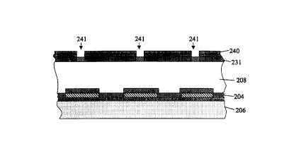
02 atmosphere at 650° C for 20 minutes to form Ti02 layer 231. Finally,
an Si02
layer 240 is deposited over layer 231 and etched to form via holes for making
electrical connections to the electrodes. Exemplary via holes are shown at 241
in
Figure 3(G).
It will be apparent to those skilled in the art that the above described
process
2o provides a structure in which the PLZT and platinum layers are isolated
from the Si02
layers. This isolation avoids the problems discussed above.
It will also be apparent to those skilled in the art that titanium may be
replaced
by magnesium or zirconium in the above described process provided the
oxidization
times are suitably reduced. Similarly, the Ti02 layer may be replaced by a
layer
comprising a PZT or PLZT material whose composition provides the electrical
insulating characteristics in question.
While the present invention has been described in terms of the construction of
a capacitor array, it will be apparent to those skilled in the art that the
present
invention may be used advantageously in any situation in which either PZT,
PLZT, or
platinum structures are to be isolated from Si02 layers to prevent cracking of
the Si02
and/or undesirable interactions between the PZT or PLZT and the Si02. Various
modifications to the present invention will become apparent to those skilled
WQ g3/~)~f30 PCT/US93A01169
X129838
in tht art from the foregoing description and accompanying drawings.
Accordingly,
the present invention is to be limited solely by the scope of the following
claims.
,
J