Note: Descriptions are shown in the official language in which they were submitted.
-
2129923
TITLE OF THE INVENTION
PROTECTION SYSTEM FOR THYRISTOR VALVE
BACKGROUND OF THE INVENTION
Field of the Invention
This invention relates to a protection system for a
thyristor valve used for DC power transmission e.t.c., and
more particularly to a protection system for a thyristor
valve which protects thyristors from volta~e stress during
the forward recovery period.
Description of the Related Art
Generally, a thyristor does not recover its forward
withstand voltage until a certain time has elapsed after the
end of power conduction. The "turn-OFF time" (Tq) is a
guide to the time required for this recovery.
When a thyristor valve is running as an inverter, the
reverse voltage period applied to the thyristor after the
end of power conduction is called the "margin angle" ( r )-
Normally, the control angle is selected to that this margin
angle r is greater than turn-OFF time Tq.
When margin angle r is smaller than turn-OFF time Tq
2129923
due to the generation of waveform distortion in the AC
system, the thyristor cannot block a forward voltage applied
following a reverse voltage, and self-fires. This
phenomenon is called "commutation failure". When thyristors
are connected in series, randomness will occur in turn-OFF
times Tq of individual thyristors. Therefore, when margin
angle r is small, there will be thyristors with and without
commutation failure. This phenomenon is called "partial
commutation failure". Thus, the whole circuit voltage will
be applied to the thyristors without commutation failure.
Therefore, when the number of thyristors with partial
commutation failure is large, a forward voltage greater than
the withstand voltage will be applied to the thyristors
which bl,ock the voltage. This will sometimes lead to
damage.
To counter this problem, in prior art, the thyristors
were protected by forcibly turning them on by supplying a
gate pulse to all the thyristors, if margin angle r became
smaller than the maximum value of turn-OFF times Tq of the
series thyristors. This is called "forced firing
protection".
The details of the above-described prior art protection
were well described in U.S. Patent No. 4,377,835 issued on
March 22, 1983 and Canadian Patent No. 1,054,218 issued on
May 8, 1979.
Such prior art forced firing protection had the
2129923
following problems. That it to say, turn-OFF time Tq
depends on the rising rate dv/dt of the applied forwardly
rising voltage v and peak value of voltage v. However, the
maximum value of turn-OFF times Tq used in prior art forced
firing protection which is taken as TqO was assumed from
rising rate dv/dt (several v/~s) in normal operation. When
an overload voltage with a larger rising rate dv/dt than in
normal operation is applied to the thyristor valve from
outside, due to a lightning surge or the action of an ON/OFF
device, turn-OFF times of individual thyristors Tq which are
taken as Tql became greater than turn-OFF time TqO. Turn-
OFF times Tql has randomness for individual thyristors in
the same way as turn-OFF time TqO.
Consequently, if a surge voltage penetrates into the
thyristor valves between the turn-OFF Times TqO and Tql
after the end of power conduction, the above forced firing
protection will not operate. However, partial commutation
failure will occur due to the randomness of turn-OFF times
Tql of individual thyristors, and there is a possibllity of
damaging the thyristors.
Also, when a forwardly rising voltage v with a large
rising rate dv/dt is applied to the thyristors, and peak
value of voltage v at that time is high, all the thyristors
connected in series will self-fire. Thus, there is a
possibility of damage due to loss at the time of turn-ON.
2129923
SUMMARY OF THE INVENTION
Accordingly, one object of this invention is to provide
a protection system for a thyristor valve which can protect
the thyristors from being damaged, even if a surge steep
voltage penetrates into the thyristor valve.
These and other objects of this invention can be
achieved by providing a protection system for a thyristor
valve composed of a plurality of thyristors connected in
series. The protection system includes a forward voltage
detection circuit connected to at least one thyristor out of
the plurality of the thyristors for detecting that a forward
voltage is applied to the thyristor to generate a forward
voltage signal, a first reverse voltage detection circuit
for detecting that a reverse voltage in excess of a first
reverse voltage level is applied to the thyristor to
generate a first reverse voltage signal, and a second
reverse voltage detection circuit for detecting that a
reverse voltage in excess of a second reverse voltage level
larger than the first reverse voltage level is applied to
the thyristor to generate a second reverse voltage signal.
The protection system further includes a protection circuit
for detecting a first time period during when the first
reverse voltage signal is outputted and a second time period
during when the first reverse voltage signal is outputted
2129923
and the second reverse voltage signal is not outputted, for
adding the first time period and the second time period to
generate an addition signal, for comparing the addition
signal with a first predetermined value to generate a
decision signal when the addition signal is smaller than the
second predetermined value, and for generating a protection
gate pulse based on the decision signal when the forward
voltage is applied to the thyristor. The protection gate
pulse is applied to all of the thyristors.
According to one aspect of this invention, there is
provided a protection system for a thyristor valve composed
of a plurality of thyristors connected in series. The
protectio,n system includes a forward voltage detection
circuit'connected to at least one thyristor out of the
plurality of the thyristors for detecting that a forward
voltage is applied to the thyristor to generate a forward
voltage signal, a first reverse voltage detection circuit
for detecting that a reverse voltage in excess of a first
reverse voltage level is applied to the thyristor to
generate a first reverse voltage signal, and a second
reverse voltage detection circuit for detecting that a
reverse voltage in excess of a second reverse voltage level
larger than the first reverse voltage level is applied to
the thyristor to generate a second reverse voltage signal.
The protection system further includes a protection circuit
2129923
for calculating a signal dependent on rising rate of a
forwardly rising voltage applied to the thyristor based on
the first reverse voltage signal and the second reverse
voltage signal when the reverse voltage is applied to the
thyristor, for comparing the rising rate dependent signal
with a second predetermined value to generate a decision
signal when the rising rate dependent signal indicates that
the rising rate is larger than a predetermined value, and
for generating a protection gate pulse based on the decision
signal when the forward voltage is applied to the thyristor.
The protection gate pulse is applied to all of the
thyristors.
It has been proved empirically that the relationship
between turn-OFF time Tq and a rising rate dv/dt of
forwardly rising voltage v is given by the following
equation.
Tq = kl . ln (dv/dt) + TO ....(1)
Here, kl and TO are constants.
Therefore, taking account of the randomness in the
characteristic of each thyristor, this invention has the
characteristic that when Equation (2) is not established,
protection is carried out through forced turn-ON by
supplying gate pulses to all the thyristors based on the
detection of rising rate dv/dt of forwardly rising voltage v
carried out by reverse voltages of two different levels of a
2129923
thyristor.
Equation (2) is obtained by substituting Equation (1)
into Equation ( r > Tq).
r > kl ln (dv/dt) + TO + Tm ....(2)
Here, Tm is a margin which takes account of the randomness
in the characteristic of a thyristor.
By providing the above means, damage to the thyristors
due to an over-voltage can be prevented, because forced
firing pulse signals are applied to all the thyristors when
an over voltage penetrates into a thyristor valve and a
forwardly rising voltage v with a steep rising rate dv/dt is
applied to the thyristors after the end of the conducting
period. I
BRIEF DESCRIPTION OF THE DRAWINGS
.A more complete appreciation of the invention and many
of the attendant advantages thereof will be readily obtained
as the same becomes better understood by reference to the
following detailed description when considered in connection
with the accompanying drawings, wherein:
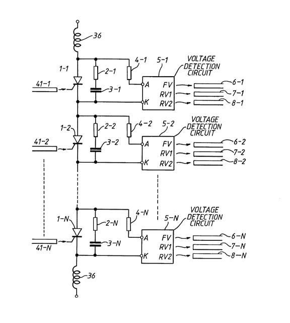
Figure 1 is a schematic diagram of a thyristor valve
and a part of a protection system thereof according to an
embodiment of this invention;
Figure 2 is a schematic diagram showing a practical
2129923
example of a voltage detection circuit shown In Figure 1;
Flgure 3 is a schematic diagram of a pulse generating
circuit which generates protection pulses according to an
embodiment of this invention;
Figure 4 is a waveform diagram for each part during
normal operation to illustrate the operation of this
embodiment; and
Figure 5 is a waveform diagram for each part during
surge voltage penetration to illustrate the operation of
this embodiment.
DETAILED DESCRIPTION OF THE PREFERRED EMBODIMENTS
Referring now to the drawings, wherein like reference
numerals designate identical or corresponding parts
throughout the several views, the embodiments of this
invention will be described below.
Figure 1 is a schematic diagram of a thyristor valve
and a part of a protection system thereof according to an
embodiment of this invention. Figure 2 is a schematic
diagram showing a practical example of a voltage detection
circuit in Figure 1. Figure 3 is a schematic diagram of a
pulse generating circuit which applies forced firing pulses
to the thyristor valve in Figure 1.
N photo-thyristors (hereafter simply "thyristors") 1-1
- 1-N are connected in series to that they will withstand a
2129923
_,
specific voltage. Snubber circuits consisting of series
connected snubber resistors 2-1 - 2-N and snubber capacitors
3-1 - 3-N are connected in parallel with thyristor 1-1 -
1-N, respectively. At the same time, DC voltage dividing
resistors 4-1 - 4-N and voltage detection circuits 5-1 - 5-N
are connected in parallel with thyristors 1-1 - 1-N,
respectively.
As simply shown as a voltage detection circuit 5 in
Figure 2, each of voltage detection circuits 5-1 - 5-N is
composed of LEDs 9, 10 and 11, Zener diodes 12 and 13,
resistors 14 and 15 and diodes 16 and 17. In Figure 2, each
of light guides 6-1 - 6-N, each of light guides 7-1 - 7-N
and each of light guides 8-1 - 8-N are simply shown as a
light guide 6, a light guide 7 and a light guide 8,
respectively.
When a forward voltage is applied to thyristors 1-1 -
1-N in Figure 1, LEDs 9 in voltage detection circuits 5-1 -
5-N emit lights. These lights are transmitted by light
guides 6-1 - 6-N to a photoelectric conversion circuit 18 in
Figure 3 which is at earth potential. Photoelectric
conversion circuit 18 converts these lights into electric
signals, which are supplied to a logic circuit 19. These
electric signals are intensified by logic circuit 19 to
become a forward voltage signal FV.
Also, when a reverse voltage of more than a specified
value VR1 (for instance, 50V) is applied to thyristors 1-1 -
21299~3
1-N, LEDs 10 emit lights which are transmitted by light
guides 7-1 - 7-N to photoelectric conversion circuit 18
which is at earth potential. These are converted into
electric signals in photoelectric conversion circuit 18,
which are intensified by a logic circuit 21 to become a
signal RV1. Furthermore, when a reverse voltage of more
than a specified value VR2 (for instance, 200V) is applied
to thyristors 1-1 - 1-N, LEDs 11 emit lights which are
transmitted by light guides 8-1 - 8-N to photoelectric
conversion circuit 18 which is at earth potential. These
are converted into electric signals in photoelectric
conversion circuit 18, which are intensified by a logic
circuit 20 to become a signal RV2. Logic circuits 19, 20
and 21 can be easily composed of OR circuits, AND circuits
or majority circuits by those skilled in the art. So that
detailed description of the circuit construction thereof may
be omitted.
Signal RV2 is inverted by an inversion circuit 22 and
causes a mono-multi circuit 24 to operate to set a flip-flop
26. Signal RV1 is inverted by an inversion circuit 23 and
causes a mono-multi circuit 25 to operate to reset flip-flop
26.
A Q output a of flip-flop 26 operates an integration
circuit 27. Signal RV1 also operates an integration circuit
28. Here, the resetting of integration circuits 27 and 28
is performed by the output signal of mono-multi circuit 25.
-- 10 --
2129923
-
The output of integration circuit 27 is applied to an
addition circuit 32 by passing through a logarithmic circuit
29 and an amplifier circuit 30 which has a specified gain.
On the other hand, the output of integration circuit 28
is applied to addition circuit 32 by passing through an
amplifier circuit 31 which has a specified gain. That is tO
say, an output c of addition circuit 32 is the sum of the
output of amplifier circuit 30 and the output of amplifier
circuit 31.
A signal generating circuit 33 is a circuit which
produces a DC signal d equivalent to kl . ln(VR2 - VR1) + TO
+ Tm. A comparator 34 inputs signal c and signal d, and its
output e is "1" when c > d.
A conduction period signal generating circuit 36
outputs a signal PHS, which is the conduction period signal
of the thyristor valve, and sets a flip-flop 35 by signal
PHS. Flip-flop 35 is reset by output e of comparator 34. A
Q output f of flip-flop 35 is inputted to an AND circuit 37.
Signal FV which is the output of logic circuit 19, is
inputted to another input terminal of AND circuit 37. When
both signal FV and signal f are "1", a mono-multi 38 is
operated and an amplifier circuit 39 is driven to cause LEDs
40-1 - 40-N to emit lights by a signal GP. These lights are
transmitted to thyristors 1-1 - 1-N via light guides 41-1 -
41-N to turn ON all thyristors 1-1 - 1-N.
The following is a description of the operation of the
-- 11 --
2129923
embodiment of this invention composed as above, with
reference to Figure 4 and 5.
Figure 4 is the waveforms of parts of a thyristor valve
during normal inverter operation. When signal PHS which is
the output of conduction period signal generating circuit 36
becomes "1" in the forward voltage period of thyristors 1-1 -
1-N , flip-flop 35 is set. In this period, signal FV of
logic circuit 19 is "1". Thus, the two inputs of AND
circuit 37 become "1" and mono-multi 38 and amplifier
circuit 39 are driven. Thus, LEDs 40-1 - 40-N emit lights
and turn ON thyristor 1-1 - 1-N. Then signal FV becomes
"O". After that, when signal PHS becomes "O", the current
flowing in this thyristor valve will commutate to the
thyristo~ valve of another phase (not illustrated),
thyristors 1-1 - 1-N in this thyristor valve are turned OFF.
During the time r after thyristors 1-1 - 1-N are turned
OFF, a reverse voltage will be applied to thyristors 1-1 - 1-
N. The reverse voltage applied to thyristors 1-1 - 1-N will
be larger than the level of voltage VR2 under the normal
condition. Therefore, as soon as thyristors 1-1 - 1-N are
turned OFF, signals RV1 and RV2 will become "1". While
signal RV1 is "1", integration circuit 28 operates and
measures a period tl in which the reverse voltage is applied
to thyristors 1-1 - 1-N. Strictly speaking, period tl is
the time when the reverse voltage is larger than voltage
VR1. But in practice, when voltage VR1 is about 50V, time
- 12 -
21299~3
_
tl can be regarded as identical with margin angle r. Also,
when the absolute value of the reverse voltage is below
voltage VR2, mono-multi 24 operates to set flip-flop 26.
Thus, integration circuit 2~ operates to measure the time t2
until the reverse voltage becomes voltage VR1 from voltage
VR2. When the reverse voltage further reduces and becomes
less than voltage VR1, flip-flop 26, integration circuit 27
and integration circuit 28 are reset to end the measurement
of time tl and time t2. The rising rate dv/dt of the
thyristor at this time can be obtained from the following
equation.
(dv/dt) = (VR2 - VR1)/t2 ....(3)
Also, since time tl can be regarded as margin angle r,
Equation.(2) can be rewritten as follows.
r = tl > kl ln [(VR2 - VR1)/ t2] + TO + Tm
tl > kl . [ln (VR2 - VR1) - ln (t2)] + TO + Tm
tl + kl . ln (t2) > kl . ln (VR2 - VR1) + TO + Tm ....(4)
In Equation (4), as opposed to the fact that the right-hand
term [kl . ln (VR2 - VR1) + tO + Tm] is constant, the left-
hand term [tl + kl . ln (t2)] varies depending on the
magnitude of the rising rate dv/dt of voltage v applied to
the thyristor. If rising rate dv/dt becomes greater,
Equation (4) will not be established.
This invention is designed to output a protection pulse
to forcibly fire all the thyristors under the conditions
when Equation (4) has not been established. That is to say,
2129923
in Figure 3, the gains of amplifiers 30 and 31 are set so
that the output of amplifier 30 is kl . ln (t2) and the
output of amplifier 31 is tl. Then, output c of addition
circuit 32 will be [tl + R1 . ln (t2)]. Output d of signal
generating circuit 33 is set so that it becomes [kl . ln
(VR2 - VR1) + TO + Tm].
During normal operation, as shown in Figure 4, output c
of addition circuit 32 at time T3 becomes greater than
output d of signal generating circuit 33. That is to say,
Equation (4) is established, and output e of comparator 34
becomes "1" and resets flip-flop 35, and the output of flip-
flop 35 becomes "O". Thus, light-emitting diodes 40-1 - 40-N
do not receive photo gate signal GP, and the operation of
the thyristor valve will proceed, as it is, to the normal
turn-ON of the next cycle.
Next, the following is a description of the case when a
surge voltage penetrates into the thyristor valve
immediately after turn-OFF, using Figure 5. Rising rate
dv/dt during the reverse voltage period becomes steep due to
the penetration of the surge voltage. Therefore, the
periods of tl and t2 become shorter. Thus, output d of
signal generating circuit 33 becomes greater than output c
of addition circuit 32, that is to say, Equation (4) is not
established, even at time T2 at which the absolute value of
the reverse voltage becomes less than voltage VR1. Output e
of comparator 34 stays "O" and flip-flop 35 is not reset.
2129923
Therefore, if a forward voltage is applied to thyristors 1-1
- l-N, signal FV becomes "1" and the output of AND circuit
37 becomes "1". Thus, light-emitting diodes 40-1 - 40-N are
driven by signal GP, and all thyristors 1-1 - l-N are fired.
According to the embodiment of this invention as
described above, protection gate pulses are transmitted to
all the thyristors. Thus, damage to the thyristors due to
an applied surge voltage can be prevented without producing
partial commutation failure.
The above description is for an example in which
voltage detection circuits which detect the forward voltage
and the reverse voltage are provided for all thyristors
which are connected in series. However, voltage detection
circuitslmay also be provided for some of the thyristors
which are connected in series.
Furthermore, an example has been described in which a
signal c which is [tl + kl . ln (t2)] is obtained by
addition circuit 32. However, a signal which is [tl + t2]
may be obtained from the addition circuit by omitting the
logarithmic circuit.
In the above-described embodiment, time t2 is obtained
by providing inversion circuit 22, mono-multi circuit 24,
flip-flop 26 and integration circuit 27. But this invention
is not limited to this embodiment. For example, instead of
these circuits another integration circuit is provided,
which integrates signal RV2 and is reset by the output
2129923
signal of mono-multi circuit 25. A subtractor is further
provided, which subtracts the output of this integration
circuit from the output of integration circuit 28. The
output of the subtractor corresponding to time period t2 is
applied to logarithmic circuit 29.
In the above-described embodiment, comparator 34
compares signal c corresponding to the value [tl + kl . ln
(t2)] with signal d corresponding to the value [kl . ln(VR2 -
VR1) + TO + Tm] in order to determine whether Equation (4)is established or not. This invention is, however, not
limited to this embodiment. The rising rate dv/dt of a
forwardly rising voltage v applied to the thyristor is
calculated by Equation (3) based on a detected time t2.
Then, it,may be possible that whether or not protection gate
pulse is to be outputted is determined by comparing rising
rate dv/dt calculated as described above with another
predetermined value, directly.
When using this invention as described above, even if a
surge voltage penetrates into a thyristor valve after turn-
OFF, rising rate dv/dt of the surge voltage is detected and
compared with the thyristor turn-OFF time. Thus, damage to
the thyristors due to an applied surge voltage can be
prevented without producing partial commutation failure by
transmitting protection pulses to all the thyristors.
- 16 -
2129923
Obviously, numerous modifications and variations of the
present invention are possible in light of the above
teachings. It is therefore to be understood that within the
scope of the appended claims, the invention may be practiced
otherwise than as specifically described herein.
- 17 -