Note: Descriptions are shown in the official language in which they were submitted.
-1- y '~~ t~ ~ ~;
RING INTERWORKING BETWEEN BIDIRECTIONAL
LINE-SWTTCHED RING TRANSMISSION SYSTEMS
Technical Field
This invention relates to ring transmission systems and, more
particularly, to interworking between bidirectional line-switched ring
transmission
systems.
Background of the Invention
It has become increasingly important to maintain communications
connectivity in the presence of transmission system failures. To this end)
ring
interworking arrangements have been proposed for transporting communications
circuits between bidirectional line-switched rings. Ring interworking is
essentially a
dual feed of communications circuits from a first ring to a second ring. The
dual
feeding takes place across two different sites, each with ring nodes for both
the first
and second rings, in order to provide the physical diversity necessary to
enable the
cross-ring communications circuits to survive a failure of one of the two
shared sites.
The second ring performs a receive switch based on some parameter or set of
parameters of the two signals being fed from the first ring. For the other
direction of
the same end-to-end cross-ring communications circuits) the second ring dual
feeds
communications circuits to the first ring. The first ring performs a receive
switch of
the two signals being fed from the second ring.
A problem arises when there is a need to groom the inter-ring
communications traffic by way of intervening wide-band digital cross-connect
systems (DCS), multiplexers (MUX) or the like, where the grooming is being
done
at a different digital signal level) i.e., bit rate, than is being used in the
rings.
Examples are DS1 digital signals in DS3 signals and VT SONET signals in STS-1
SONET signals. In such arrangements, if a failure occurs incoming to the DCS,
ML1X or other grooming apparatus from one ring, it will not be recognized by
the
other ring because the inter-ring grooming apparatus will only insert the DS 1
or VT
failure indication and not the DS3 or STS-1 failure indication. Consequently,
the
inter-ring groomed signals, i.e., DS3s or STS-1 s, passed off to either ring
could
appear to be "good" but could, in fact, contain corrupted or failed lower
level digital
signals, i.e., DSIs or VTs.
-2-
One attempt at avoiding the problems associated with inter-ring
grooming of lower level digital signals in the higher level digital signals
employed in
interworlcing path-switched rings is described in a contribution to T1
Standards
Project T1X1.2 entitled "SWB Ring Interconnection Architecture Issues and
Proposed Interim Solutions", T1X1.2f93-013, dated March 1, 1993. If the path-
switched ring solution proposed in the noted Contribution T1X1.2/93-013 were
to be
applied to interworking bidirectional line-switched rings, the result would be
an
inefficient arrangement requiring the use of additional service bandwidth
between
the shared interworking nodes, the use of additional equipment in the nodes
and the
use of more interface and grooming capacity in the inter-ring grooming
apparatus.
Summary of the Invention
The problems related to the possibility of passing off apparent "good"
higher level, i.e., bit rate, digital signals that may include corrupted or
failed lower
level, i.e., bit rate, digital signals because of inter-ring grooming of the
lower level
digital signals from one bidirectional line-switched ring to another
bidirectional
line-switched ring employing at least a first shared node and a second shared
node
are overcome by dual feeding communications circuits from one line-switched
ring
to the other via the shared nodes, by provisioning at least one inter-ring
groomed
communications circuit from a secondary ring node of one of the shared nodes
(secondary communications circuit) of a particular ring to be supplied to a
primary
ring node in the other shared node of the same ring and provisioning the
primary ring
node so that the at least one supplied secondary communications circuit is a
candidate to be selected as a through communications circuit. Additionally, a
replica
of the at least one secondary communications circuit is obtained in the
primary ring
node and demultiplexed to obtain the lower level digitals signals therefrom.
Then,
the lower level digital signals in the at least one secondary communications
circuit
are evaluated on a one-to-one pairwise basis with corresponding lower level
digital
signals in a corresponding communications circuit (primary communications
circuits) being supplied from the inter-ring grooming apparatus associated
with the
primary ring node. The selected lower level digital signals are combined into
a
"new" primary communications circuit which is added in the primary ring node
via a
selector into the transmission path.
The selector in the primary ring node is revertively biased to normally
select the "new" primary communications circuits in order to protect against
selecting secondary communication circuits as through communications circuits
in
the primary ring node when there is an interconnect or other failure to the
inter-ring
_ 3 _ ''~ ,~ ~ .a'
grooming apparatus in the shared node supplying the secondary communications
circuits. The provisioning of the primary ring node and the secondary ring
node is
such that the demultiplexing to obtain the lower level digital signals, their
evaluation
and selection, and multiplexing only need be done in the primary ring node and
not
in both.
Specifically, the inter-ring groomed at least one secondary
communications circuit is demultiplexed to obtain the lower level digital
signals.
The primary and corresponding secondary lower level digital signals are
evaluated
on a one-to-one pairwise basis to determine the "best" signal of each pair.
Then, the
determined best lower level digital signals are selected by selectors to be
multiplexed
into a "new" primary inter-ring groomed communications circuit. The "new"
primary communications circuit is then normally selected in the primary ring
node to
be added to the transmission path. However, in the case of an interconnect or
other
failure in the primary ring node the revertive selector selects the at least
one
communications circuit to the termination ring node for the primary ring node.
Upon the failure being corrected, the revertive selector automatically reverts
back to
selecting the "new" primary communications circuit to the termination ring
node.
Brief Description of the Drawing
In the drawing:
FIG. 1 shows, in simplified block diagram form, a bidirectional line-
switched ring transmission system interworking with another bidirectional line-
switched ring transmission system including inter-ring grooming;
FIG. 2 shows, in simplified block diagram form, details of a ring node
which may be employed in the practice of the invention;
FIG. 3 shows, in simplified block diagram form, details of a squelcher
used in the ring node of FIG. 2;
FIG. 4 shows, in simplified block diagram form, details of an AIS insert
unit employed in the squelcher of FIG. 3;
FIG. 5 is an exemplary ring node ID table included in memory of the
controller of FIG. 2;
FIG. 6 is an exemplary communications circuit B7 table also included in
memory of the controller of FIG. 2 for ring node 111;
FIG. 7 is a flow chart illustrating the squelch and switch operation of the
controller of FIG. 2;
-4_ _ _
FIG. 8 illustrates the "normal" operation in bidirectional line-switched
ring 100 including the first and second shared nodes;
FIG. 9 shows, in simplified block diagram form, a DCS including
apparatus embodying an aspect of the invention;
FIG. 10 shows, in simplified block diagram form, a DCS and an adjunct
apparatus including an aspect of the invention; and
FIG. 11 illustrates the operation in bidirectional line-switched ring 100
in the presence of a failure of a so-called hand-off link to the first ring
node 112.
Detailed Description
FIG. 1 shows, in simplified form, bidirectional line-switched ring
transmission system 100 interworking with another bidirectional line-switched
ring
transmission system 101. In this example) bidirectional line-switched ring 100
includes ring nodes 110 through 115) and the other bidirectional line-switched
ring
101 includes ring nodes 120 through 125. Ring nodes 112 and 120 form first
shared
node 130 for interworking communications circuits between bidirectional line-
switched ring 100 and bidirectional line-switched ring 101. Similarly, ring
nodes
114 and 125 form an additional shared node 131 for interworking communications
circuits between bidirectional line-switched ring 100 and bidirectional line-
switched
ring 101. In this example, ring nodes 112 and 120 in shared node 130 are shown
as
being interconnected by inter-ring grooming apparatus, namely, digital cross-
connect
system (DCS) 132. Similarly, ring nodes 114 and 125 in shared node 131 are
shown
as being interconnected by inter-ring grooming apparatus, namely, digital
cross-
connect system (DCS) 133. Both DCS 132 and DCS 133 are so-called wide-band
cross-connect systems of a type known in the art and described in the
Technical
Reference entitled "Wideband and Broadband Digital Cross-Connect Systems
Generic Requirements and Objectives", TR-TSY-000233, Issue 2, September 1989,
Bell Communications Research. It will be apparent that other wide-band
grooming
apparatus may be equally employed to realize the inter-ring grooming of
communications circuits. One other such inter-ring grooming apparatus is a
wide-
band digital multiplex system, for example, the DDM-2000 Multiplex System
available from AT&T Company.
Ring nodes 110 through 115 are interconnected by transmission path
116 in a counter-clockwise direction and by transmission path 117 in a
clockwise
direction to form bidirectional line-switched ring 100. In this example,
transmission
paths 116 and 117 are comprised of optical fibers and each could be comprised
of a
single optical fiber or two (2) optical fibers. That is, bidirectional line-
switched ring
~~r~~~_
transmission system 100 could be either a two (2) optical fiber or a four (4)
optical
fiber system. In a two (2) optical fiber system, each of the fibers in
transmission
paths 116 and 117 includes service bandwidth and protect:~on bandwidth. In a
four
(4) optical fiber system, each of transmission paths 116 an~i 117 includes an
optical
fiber for service bandwidth and a separate optical fiber for protection
bandwidth.
Such bidirectional line-switched ring transmission systems are known.
Similarly,
ring nodes 120 through 125 are interconnected by transmission path 128 and by
transmission path 129 to form bidirectional line-switched ring 101. In this
example,
transmission of digital signals in the SONET digital si;nal format is assumed.
However, it will be apparent that the invention is equally applicable to other
digital
signal formats, for example, the CCITT synchronous digits 1 hierarchy (SDH)
digital
signal formats. In this example, it is assumed that an opti~:al OC-N SONET
digital
signal format is being utilized for transmission over transrr,ission paths 116
and 117
in bidirectional line-switched ring 100 and a similar or som ~ other digital
signal over
transmission path 128 in bidirectional line-switched ring 101. The SONET
digital
signal formats are described in a Technical Advisory entitled "Synchronous
Optical
Network (SONET) Transport Systems: Common Generic Criteria", TA-NWT-
000253, Bell Communications Research, Issue 6, September 1990.
For purposes of this description, a "communications circuit" is
considered to be a SONET STS-3 digital signal having its entry and exit points
on
the particular ring. However, for brevity and clarity of exposition, the inter-
ring
grooming will be described using STS-1 SONET signals as the higher level
signals
and VT SONET signals as the lower level signals. Al;ain, other digital signal
formats may be equally employed. Another example of svlch digital signal
formats
are the known DS3 and DS 1 digital signals. Additionally, the SDH STM and SDH
VC lower order digital signal formats could equally be employed.
It is noted that requests and acknowledgments for protection switch
action, in bidirectional line-switched rings 100 and 101, are transmitted in
an
automatic protection switch (APS) channel of the protection bandwidth on each
of
transmission paths 116 and 117 for ring 100 and on each ~~f transmission paths
128
and 129 for ring 101. The APS channel, in the SONET ~-'ormat, comprises the Kl
and K2 bytes in the SONET overhead of the protection bandwidth. The Kl byte
indicates a request of a communications circuit for switch action. The first
four (4)
bits of the KI byte indicate the type of switch and the last four (4) bits
indicate the
ring node identification (ID). The K2 byte indicates an acknowledgment of the
requested protection switch action. The first four (4) bits of the K2 byte
indicate the
6- '~1 ,~_>.~~
ring node >I7 and the last 4 bits indicate the action taken.
Each of ring nodes 110 through 115 and 120 through 125 comprises an
add-drop multiplexer (ADM). Such add-drop multiplexer arrangements are known.
For generic requirements of a SONET based ADM see the Technical Reference
entitled "SONET ADD-DROP Multiplex Equipment (SONET ADM) GENERIC
CRITERIA") TR-TSY-000496, Issue 2, September 1989, Supplement 1, September
1991, Bell Communications Research. In this example, the ADM operates to pass
signals through the ring node, to add signals at the ring node, to drop
signals at the
ring node, to bridge signals during a protection switch and to loop-back-
switch
signals during a protection switch at the ring node.
It should be noted that each of ring nodes 110 through 115 and ring
nodes 120 through 125 are provisioned with the identities of all active
communications circuits including those being added and/c>r dropped at the
node and
those passing through. Additionally, those ring interworking communications
circuits terminated in shared nodes 130 and 131 are provisioned as such
communications circuits. The provisioning of, for example, loop-back-
switching
node 111 is shown in FIGs. 5 and 6 and described below. It is noted that ring
node
111 is the loop-back-switching ring node for ring node 112 in shared node 130.
To
this end, ring node 111 is provisioned to provide a secondary communications
circuit
connection for any ring interworking communications circuits terminating in
ring
node 112 to ring node 114 in additional shared node 131 ) when ring node 112
has
failed. This secondary communications circuit is established on a
communications
circuit-by-communications circuit basis by controllably allowing the loop-back-
switching of communications circuits terminated in ring node 112 to ring node
114
and by controllably not squelching those communications circuits.
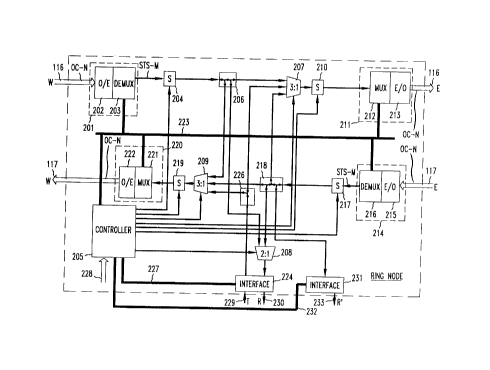
FIG. 2 shows, in simplified block diagram form, details of ring nodes
110 through 115 and ring nodes 120 through 125. In this example, a west (V~-to-
east (E) digital signal transmission direction is assumed in the service
bandwidth and
the protection bandwidth on transmission path 116. It will be apparent that
operation
of the ring node and the ADM therein would be similar for an east (E) - to -
west
(V~ digital signal transmission direction in the service bandwidth and the
protection
bandwidth on transmission path 117. Specifically, shown is transmission path
116
entering the ring node and supplying an OC-N SONET optical signal to receiver
201,
where N could be, for example, 3, 12 or 48. Receiver 201 includes an
optical/electrical (O/E) interface 202 and a demultiplexer (DEMUX) 203, which
yields at least one (1) STS-M SONET digital signal. Such O/E interfaces and
-7-
demultiplexers are known. In this example, M is assumed to be three (3) and N
is
greater than M. The STS-M signal output from DEMUR 203 is supplied to
squelcher (S) 204, which under control of controller 205, controllably
squelches, i.e.,
blocks, particular incoming communications circuits. Details of squelcher (S)
204
are shown in FIGS. 3 and 4 and its operation is described below. Thereafter)
the
STS-M signal, squelched or otherwise, is supplied to broadcast element 206. A
broadcast element replicates the STS-M signal supplied to it and supplies the
replicated signals as a plurality of individual outputs. Such broadcast
elements are
known. Broadcast element 206 generates three identical STS-M signals and
supplies
one STS-M signal to an input of 3:1 selector 207, a second STS-M signal to an
input
of 2:1 selector 208 and a third STS-M signal to an input of 3:1 selector 209.
An
STS-M signal output from 3:1 selector 207 is supplied to squelcher (S) 210,
which is
identical to squelcher (S) 204. Squelcher (S) 210 is employed, under control
of
controller 205, to squelch particular outgoing communications circuits. The
STS-M
signal output from squelcher (S) 210 is supplied to transmitter 211 and,
therein, to
multiplexer (MUX) 212. The output of MUX 212 is an electrical OC-N digital
signal, which is interfaced to transmission path 116 via electrical/optical
(E/O)
interface 213. Such multiplexers (MUXs) and electrical/optical (E/O)
interfaces are
well known.
Similarly, in the east (E) - to - west (V~ direction an OC-N optical
signal is supplied via transmission path 117 to receiver 214 and, therein, to
optical/electrical (O/E) interface 215. In turn, demultiplexer (DEMUR) 216
yields a
STS-M signal which is supplied via squelcher (S) 217 to broadcast element 218.
Broadcast element 218 replicates the STS-M signal into a plurality of
identical STS-
M signals, in this example, four (4). One STS-M signal is supplied to an input
of 3:1
selector 207, a second STS-M signal is supplied to an input of 2:1 selector
208, a
third STS-M signal is supplied to an input of 3:1 selector 209 and a fourth
STS-M
signal is supplied to interface 231. An output from 3:1 selector 209 is
supplied via
squelcher (S) 219 to transmitter 220. In transmitter 220, multiplexer (MUX)
229
multiplexes the STS-M into an electrical OC-N and, then, electrical/optical
(E/O)
interface 222 supplies the optical OC-N signal to transmission path 117.
Thus, in this example, broadcast element 218 supplies the secondary
communications circuits from the additional shared node as candidates for
through
circuits and also drops the secondary communications circuits via interface
231
under control of controller 205. It should be noted that although the
communications
circuits are SONET STS-3 digital signals, interface 231 and interface 224 drop
~~.~~,~~?~
_g_
SONET STS-1 digital signals. Similarly, STS-1 digital signals are combined in
the
interfaces to form STS-3 digital signals) in known fashion. Additionally, it
is noted
that selector 208 selects on a STS-1 level. To this end, the STS-3 digital
signals are
demultiplexed in selector 208 to obtain the three STS-1 digital signals, the
STS-1
signals are selected and then multiplexed back into a STS-3 signal, which is
supplied
to interface 224. Selector 209 in revertively biased under control of
controller 205,
to normally select the STS-M signal being supplied from interface 224.
Controller 205 operates to effect squelching of communications circuits
and to selectively allow communications circuit connections to ring node 114
in
shared node 131 for communications circuits terminating in ring node 112, when
ring node 112 in shared node 130 has failed. Controller 205 communicates with
demultiplexers 203 and 216 and multiplexers 212 and 221 via bus 223 and with
interface 224 via bus 227. Specifically, controller 205 monitors the incoming
digital
signals to determine loss-of-signal, alarm conditions, presence of alarm
indication
signal (AIS), SONET format K bytes and the like. Additionally, controller 205
causes the insertion of appropriate K byte messages for protection switching
purposes, examples of which are described below. To realize the desired
deterministic squelching of the communications circuits, and the selective
allowing
of communications circuit connections to ring node 114 for circuits
terminating in
ring node 112) controller 205 is advantageously provisioned via 228 with the
identities (IDs) of all the ring nodes in bidirectional line-switched ring 100
and the
identities of all the communications circuits passing through the ring node,
including
those terminated in a ring interworking node, as well as, those communications
circuits being added and/or dropped at the ring node. The squelching of
communications circuits and the selective allowance of communications circuit
connections to ring node 114 when ring node 112 has failed, under control of
controller 205 is described below. Additionally, controller 205 controls the
dropping, via interface 231, of the secondary communications circuits being
supplied
from the secondary ring node of shared node 131 (FIG. 1 ) and the revertive
biasing
of selector 209 to normally select the STS-M signal from interface 224 to be
added
in transmission path 117. Under abnormal conditions) i.e., a failure or the
like, of
the STS-M signal being supplied from interface 224, selector 209 is controlled
to
select a secondary communications circuit being supplied from ring node 114,
which
is the secondary communications circuit being supplied to interface 231. Upon
the
failure being corrected or otherwise alleviated, selector 209 automatically
reverts
back to selecting a new primary communications circuit from interface 224.
r
-9-
Interface 224 is employed to interface, in this example, to the particular
inter-ring grooming apparatus being employed. As indicated above, in this
example
both interface 224 and interface 231 between STS-3 digital signals to STS-1
digital
signals, in known fashion. Specifically, an STS-3 digital signal to be dropped
at the
ring node is supplied to interface 224 via 2:1 selector 208, under control of
controller
205, from either broadcast element 206 or broadcast element 218. This STS-3
signal
is demultiplexed in interface 224 and supplied as three (3) STS-1 signals (R)
to
circuit path 230. Similarly, an STS-3 secondary communications circuit being
supplied, via broadcast element 218, to interface 231 is demultiplexed
therein, under
control of controller 205) and supplied as three (3) STS-1 signals (R') to
circuit path
233. A signal (T) to be added at the ring node is supplied to interface 224
where it is
converted to the STS-M digital signal format) if necessary. The STS-M digital
signal is then supplied to broadcast element 226 where it is replicated. The
replicated STS-M digital signals are supplied by broadcast element 226 to an
input
of 3:1 selector 207 and an input of 3:1 selector 209. In this example, 3:1
selectors
207 and 209, under control of controller 205, select the signal being added
for
transmission in the service or protection bandwidth on either transmission
path 116
or transmission path 117.
It should be noted that, in this example, the normal transmission path for
a duplex digital signal being added at the ring node would be in the service
bandwidth on transmission path 116 and transmission path 117, for example,
towards the west (V~. If there were to be a protection switch, the signal (T)
being
added from interface 224 would be bridged via broadcast element 226 and chosen
by
3:1 selector 207, under control of controller 205, to the protection bandwidth
on
transmission path 116. Similarly, if there were to be a loop-back protection
switch
and the ring node was adjacent to the failed ring node, the signal (R) to be
dropped at
the ring node would be received in the protection bandwidth on transmission
path
117 and would be switched from broadcast element 218 via 2:1 selector 208 to
interface 224. Otherwise, the signal (R) to be dropped would be switched in a
ring
node adjacent the failure from the protection bandwidth on transmission path
117 to
the service bandwidth on transmission path 116 and received at the ring node
in
usual fashion. Then, the signal (R) being dropped from transmission path 116
is
supplied via broadcast element 206 and 2:1 selector 208 to interface 224.
Controller 205 controls and monitors the status of interface 224 and the
digital signals being supplied thereto via bus 227 and controls and monitors
interface
231 via bus 232. Specifically, controller 205 monitors interface 224 for loss-
of
__ ~~~~~~ ~,
- to -
signal, coding violations and the like.
Under control of controller 205, digital signals may be passed through,
added at, dropped at, bridged at or loop-back-switched at the ring node. In
ring node
112 of shared node 130, a drop and pass-on of a first transmission direction
of a
duplex communications circuit is realized, under control of controller 205 by
broadcast element 206 and 3:1 selector 207. To this end, broadcast element 206
replicates the STS-M digital signal and supplies one of the resulting STS-M
digital
signals to 2:1 selector 208 and another STS-M to 3:1 selector 207. In this
manner,
the same STS-M digital signal is available to be dropped in ring node 112 and
passed-on to ring node 114. If interface 224 or the hand-off duplex link to
interface
224 in ring node 112 fails, a good STS-M is still supplied in ring node 114 to
ring
node 125 of ring 101 in shared node 131. A loop-back-switch of an STS-M
digital
signal incoming in the service bandwidth on transmission path 116 is effected
by
controller 205 causing 3:1 selector 209 to select the STS-M digital signal
from
broadcast element 206 and supplying it via squelcher (S) 219 to transmitter
220. In
turn, transmitter 220 supplies an OC-N optical signal to the protection
bandwidth on
transmission path 117. Note that when used as a primary node and a loop-back-
switch is being made via selector 209 that selector 207 must be provisioned to
select
the same STS-M digital signal as selector 209. It will be apparent that in the
loop-
back-switch operation, if the signal is incoming in service bandwidth on
transmission path 116, it will be loop-back-switched to the protection
bandwidth on
transmission path 117 and vice versa, except for communications circuits being
added and/or dropped at the ring node. If the signal is incoming in the
protection
bandwidth on transmission path 116, it will be loop-back-switched to the
service
bandwidth on transmission path 117 and vice versa. A signal to be added at the
ring
node is supplied from interface 224, replicated via broadcast element 226 and
selected either by 3:1 selector 207 or 3:1 selector 209, under control of
controller
205, to be added on transmission path 116 or transmission path 117,
respectively.
Again) note that selector 209 is biased under control of controller 205 to
normally
select the STS-M signals being supplied from interface 224. Additionally, if
there
was a failure of the inter-ring grooming apparatus and/or the hand-off thereto
in this
node, the secondary communications circuits supplied via broadcast element 218
would be selected as through circuits by selector 209 under control of
controller 205.
A digital signal to be dropped at the ring node is selected by 2:1 selector
208, under
control of controller 205, either from broadcast element 206 (transmission
path 116)
or broadcast element 218 (transmission path 117). The pass-through and loop-
back
__
-11-
functions for a signal incoming on transmission path 117 is identical to that
for an
incoming signal on transmission path 116. In ring node 112 of shared node 130,
the
replication of the duplex communications circuit from ring node 114 of shared
node
131 for circuits intended to be added in ring node 112, is realized under
control of
controller 205, by 3:1 selector 209 selecting an incoming signal from ring
node 114
when either interface 224 or the hand-off duplex link in ring node 112 fails.
It is
noted, that when the node is used as a secondary node, no special functions
and no
special provisioning are required.
Possible communications circuit misconnections are avoided in
bidirectional line-switched ring 100, by deterministically squelching each
communications circuit terminated in a failed ring node, other than a
communications circuit terminated in its primary interworking ring node) in
ring
loop-back-switching nodes adjacent to the failed ring nodes(s). A primary
interworking ring node for a communications circuit is provisioned to
broadcast the
communications circuit to a secondary interworking ring node and to
controllably
select a communications circuit from the secondary interworking ring node. In
this
example, the primary interworking ring node is the ring node at which a
communications circuit is intended to be transported to and from ring 101. To
this
end, each ring node in bidirectional line-switched ring transmission system
100 is
typically equipped to effect the desired squelching via squelchers (S) 204,
210, 217
and 219, under control of controller 205. In this example, both incoming and
outgoing communications circuits are squelched, however, it may only be
necessary
to squelch outgoing communications circuits.
Additionally, in this example) ring nodes 111 and 113 adjacent ring
node 112 in shared nodes 130 are provisioned to selectively allow a secondary
communications circuit connection to ring node 114 in secondary shared node
131
for communications circuits terminated in ring node 112, when ring node 112
fails.
This secondary communications circuit connection is realized by not squelching
the
communications circuits terminated in ring node 112 in adjacent nodes 111 and
113
when ring node 112 fails. Instead, the communications circuits terminated in
ring
node 112 in their primary shared node 130 are loop-back-switched in ring nodes
111
and 113 and supplied to ring node 114 in their secondary shared node 131. It
should
be noted, however, if either ring node 114 in shared node 131 or the ring node
terminating the communications circuit in ring 100 has also failed, then the
communications circuits terminated in their primary interworking ring node 112
are
squelched.
-12- '~ v~
FIG. 3 shows, in simplified block diagram form, details of an exemplary
squelcher (S) unit. Specifically, the STS-M digital signal is supplied to
demultiplexer (DEMUX) 301 where it is demultiplexed into its constituent M STS-
1
digital signals 301-1 through 302-M. The M STS-1 digital signals are supplied
on a
one-to-one basis to AIS insert units 303-1 through 303-M. AIS insert units 303-
1
through 303-M, under control of controller 205, insert the AIS in the STS-1
digital
signals included in the communications circuits, i.e., STS-M digital signals,
to be
squelched. Details of AIS insert units 303 are shown in FIG. 4 and described
below.
Thereafter, the M STS-1 digital signals are multiplexed in multiplexer (MUX)
304 to
yield the desired STS-M digital signal. The details of multiplex schemes for
the
STS-M digital signal are described in the technical advisory TA-NWT-000253,
noted above.
FIG. 4 shows, in simplified block diagram form, details of AIS insert
units 303. Specifically, shown is a STS-1 digital signal being supplied to AIS
generator 401 and to one input of 2:1 selector 402. AIS generator 401 operates
to
insert AIS in the STS-1 digital signal. As indicated in the technical advisory
TA-
NWT-000253, the STS path AIS is an all ones {1's) signal in the STS-1 overhead
bytes H1, H2 and H3 and the bytes of the entire STS SPE (synchronous payload
envelope). Selector 402 selects as an output, under control of controller 205,
either
the incoming STS-1 digital signal or the STS-1 digital signal with AIS
inserted from
AIS generator 401.
FIG. 5 is a table including the identification (ID) of ring nodes 110
through 115 for bidirectional line-switched ring 100. The ring node IDs are
stored in
a look-up table which is provisioned via 228 in memory of controller 205 (FIG.
2).
FIG. 6 is illustrative of a table including the identification of all the
active communications circuits in a ring node, in this example, ring node 111
for a
counter-clockwise orientation of nodes 110 through 115. The active
communications circuits include those being added, being dropped or passing
through ring node 111 and, additionally, those terniinated in an interworking
ring
node. The table including the IDs of the active communications circuits in the
ring
node are provisioned via 228 in a look-up table in memory of controller 205.
Shown
in the table of FIG. 6 are the STS-M communications circuit numbers (#) a
through
d, the ring node including the communications circuit entry point, i.e., the A
termination for the communications circuit, and the ring nodes) including the
communications circuit exit point(s), i.e., the Z termination(s) for the
communications circuit and whether the communications circuit is an
interworking
r~ ~ l~.t
-13-
communications circuit. An interworking communications circuit is one which
has
terminations in both bidirectional-line switched ring 100 and bidirectional
line-
switched ring 101. A communications circuit terminated in its primary
interworking
ring node 112 in shared node 130 is shown as being broadcast to its secondary
interworking ring node 114 in shared node 131 and identified in the
provisioning as
being a ring interworking communications circuit. Thus, the communications
circuit
ID table of FIG. 6, shows that STS-M(a) enters ring 100 at ring node 110 and
exits
ring 100 at ring node 111, and is not a ring interworking communications
circuit.
STS-M(b) enters ring 100 at ring node 111 and exits at ring nodes 113 and is
not a
ring interworking communications circuit. STS-M(c) enters ring 100 at ring
node
110 and normally exits at ring node 112, and is a interworking communications
circuit. If interworking ring node 112 fails) the communications circuits
terminated
in it will not be squelched in adjacent ring nodes 111 and 113, but will be
supplied
via loop-back-switching to its secondary interworking ring node 114. Provided,
however, that neither the secondary interworking ring node 114 for the
communications circuit nor the ring node terminating the communications
circuit in
ring 100 has also failed. STS-M(d) enters ring 100 at ring node 111 and exits
at ring
node 115. Although the ring nodes designated A terminations are considered
entry
points and the ring nodes designated Z terminations are considered exit
points, it will
be apparent that the individual communications circuits may be duplex circuits
having entry and exit points at each such node. It should be noted that
heretofore
only the communications circuits being added and/or dropped at the node were
provisioned therein. Additionally, it is noted that primary interworking ring
node
112 is provisioned such that it will normally be adding the communications
circuits
being supplied thereto via path 229 and interface 224 (FIG. 2). If the inter-
ring
grooming apparatus, circuit paths to the inter-ring grooming apparatus,
interface 224
or circuit path 229 fail, then the through candidate communications circuits
being
supplied from secondary interworking ring node 114 are selected via selector
209
(FIG. 2). Again, the revertive selection is important so that "good" "new"
inter-ring
groomed STS-M communications circuits are added in the transmission path in
primary interworking ring node 112. However, when the failure is removed
primary
interworking node 112 will again revert to adding the communications circuits
being
supplied via path 229 and interface 224.
FIG. 7 is a flow chart illustrating the operation of controller 205 in
controlling the operation of the ring nodes in order to effect the
deterministic
squelching of communications circuits and the selective provisioning of the
-14- ~:1J~J~v7
secondary duplex communications circuit connections) to secondary interworking
ring node 114 for communications circuits terminated in their failed primary
interworking ring node 112. Specifically, the process is entered via step 701.
Then,
operational block 702 causes the K bytes of an incoming OC-N signal to be
observed
and processes the ring node 117s therein. Then, conditional branch point 703
tests to
determine if the processed ring node IDs indicate that one or more ring nodes
have
failed. Again, a ring node failure is defined as to include node equipment
failure and
so-called node isolation failure caused by fiber cuts and the like. Specific
examples
of failure conditions are discussed below. Thus) if the processed ring node
IDs
indicate no ring node failure, the failure is other than a ring node and
operational
block 704 causes the usual bidirectional ring bridging and switching to be
effected.
Thereafter, the process is ended via step 705. If the processed ring node IDs
indicate
a multiple ring node failure) operational block 706 causes the failed ring
node IDs to
be obtained from the ring node >D look-up table in memory. Then) control is
passed
to operational block 707 which causes the identity (>D) of the affected
communications circuits to be obtained from the communications circuit ID look-
up
table in memory. If step 703 indicates a single ring node failure, the failed
ring node
ID is already known and control is passed directly to step 707. Once the
affected
communications circuits are identified, operational block 708 causes the
appropriate
ones of squelchers (S) 204, 210, 217 and 219 (FIG. 2), in this example, to
squelch
those identified communications circuits in the ring node. As indicated above,
all
communications circuits active in this ring node that are terminated in a
failed ring
node are squelched. For the purpose of squelching a broadcast communications
circuit, only the first "A" and last "Z" terminations are used to trigger the
squelching.
A ring interworking communications circuit is treated, for the purpose of
squelching,
just like a broadcast communications circuit from its termination in
bidirectional
line-switched ring 100 to its primary shared node and secondary shared node.
Operational block 704 causes the communications circuits not terminated in the
failed ring nodes) to be bridged and switched to "heal" the ring. Thereafter,
the
process is ended in step 705.
FIG. 8 illustrates in simplified form a "normal" ring interworking
communications circuit connection in bidirectional line-switched ring 100.
Specifically, the communications circuit connection is between ring node 110,
the A
termination, and its primary interworking ring node 112. Thus) one portion (T
A ) of
the duplex communications circuit enters ring 100 at ring node 110 and is
supplied
in the service bandwidth of transmission path 116 through ring node 111 to its
-ls-
primary interworking ring node 112. The received portion of the communications
circuit is normally handed-off as R p in ring node 112. However, the received
portion is also passed along through ring node 113 to also be received at its
secondary interworking ring node 114 as R S . Similarly, another portion (T p
) of the
s duplex communications circuit normally enters ring 100 at its primary
interworking
ring node 112 and is selected to be supplied to the service bandwidth of
transmission
path 117. In transmission path 117, this portion of the communications circuit
is
passed through ring node 111 and received as RA at ring node 110.
Additionally,
this portion of the communications circuit is supplied as T S from secondary
interworking ring node 114 in the service bandwidth of transmission path 117
through ring node 113 and is available as a candidate to be selected for
transmission
at primary interworking ring node 112. The communications circuit T S is also
dropped at primary ring node 112 as unidirectional communications circuit R~P
.
Then communications circuit R~P is available so that the lower level digital
signals
1 s may be obtained for comparison and selection. As indicated above, this
selection of
T $ occurs if the hand-off link fails in primary interworking ring node 112.
It should
be noted that ring node 112 can be provisioned to normally select the
communications circuit T S from ring node 114.
Although not specifically shown in FIG. 7) it is noted that if the hand-off
link fails in the primary interworking ring node 112 for a communications
circuit,
the affected communications circuit or portion of it is being broadcast along
to be
obtained in the secondary interworking ring node 114 for the communication
circuit.
Specifically, if the receive (Rp) portion of the hand-off link fails in
primary
interworking ring node 112, it is passed along via broadcast element 206 and
3:1
selector 207 (FIG. 2) and selected to be handed-off as R S in secondary
interworking
ring node 114. Similarly, if the transmit (Tp) portion of the hand-off link
fails in
primary interworking ring node 112, controller 20s in ring node 112 causes 3:1
selector 209 (FIG. 2) to select the transmit (T s ) portion of the
communications
circuit from secondary interworking ring node 114.
FIG. 9 shows, in simplified block diagram form, a digital cross-connect
system (DCS) including apparatus embodying an aspect of the invention. It is
noted
that for brevity and clarity of description only one direction of signal
transmission is
shown and only one digital signal will be considered. It will be apparent to
those
skilled in the art that there is a similar opposite direction of transmission
and that a
relatively large number of digital signals would normally be groomed by such a
DCS. Again, in this example, a SONET STS-1 digital signal is being groomed at
the
- 16-
lower VT digital signal level. Specifically, shown is an STS-1 signal (T')
being
supplied from ring node 120 (FIG. 1) in bidirectional line-switched ring 101
to DCS
132 and therein to demultiplexer (DEMUX) 901. DEMUX 901 demultiplexes the
STS-1 signal to obtain the VT signals in known fashion. The VT signals are
supplied to time slot interchanger (TSI) 902 where they are groomed under
control
of controller 903. 'Then) the groomed VT signals are supplied on a one-to-one
basis
to 2:1 selectors 904-1 through 904-Y, where Y is the number of VT signals
being
transported by the STS-1 signal. Similarly, a corresponding inter-ring groomed
STS-1 signal (R') supplied from secondary interworking ring node 114 in shared
node 131 is demultiplexed in demultiplexer (DEMUX) 905 to obtain VT signals
which correspond on a one-to-one basis with the VT signals being supplied to
selectors 904 from TSI 902. The VT signals from DEMUX 905 are supplied on a
one-to-one basis to other inputs of selectors 905-1 through 905-Y. Controller
903
evaluates the VT signals on a pair-wise basis, in this example, in both DEMUX
901
and DEMUX 905) to determine the best VT signal in each pair and, then, causes
selectors 904 to select the best VT signals. The evaluation may include
monitoring
the VT signals for loss of signal, AIS and/or bit error rate. The selection of
the VT
signals is such that the corrupted and/or failed VT signals are not selected.
Thereafter, the selected VT signals are combined via multiplexer (MUX) 906 to
obtain the desired inter-ring groomed STS-1 signal (T).
FIG. 10 shows, in simplified block diagram form another arrangement
embodying an aspect of the invention. Specifically, shown are DCS 1001 and
selector unit 1002 which form inter-ring grooming apparatus 132. It is noted
that for
brevity and clarity of description only one direction of signal transmission
is shown
and only one digital signal will be considered. It will be apparent to those
skilled in
the art that there is a similar opposite direction of transmission and that a
relatively
large number of digital signals would normally be groomed by such a DCS.
Again,
in this example, a SONET STS-1 digital signal is being groomed at the lower VT
digital signal level. DCS 1001 includes controller 1003, DEMUX 1004, TSI 1005
and MUX 1006 and operates in known fashion to groom STS-1 signals at the VT
signal level. Specifically, shown is an STS-1 signal (T') being supplied from
ring
node 120 (FIG. 1 ) in bidirectional line-switched ring 101 to DCS 1001 and
therein to
DEMUX 1004. DEMUX 1004 demultiplexes the STS-1 signal to obtain the VT
signals in known fashion. The VT signals are supplied to TSI 1005 where they
are
groomed under control of controller 1003. Then, the groomed VT signals are
supplied to MUX 1006 where they are combined into a groomed STS-1 signal (T~~
).
~~~~9~'~
-17-
The groomed STS-1 signal T ~ is supplied to selector unit 1002 and therein to
DEMUR 1007. DEMUR 1007 demultiplexes the groomed STS-1 signal T~~ to
obtain the VT signals. The, the VT signals are supplied on a one-to-one basis
to first
inputs of 2:1 selectors 1008-1 through 1008-Y, where Y is the number of VT
signals
being transported by the STS-1 signal. Similarly, a corresponding inter-ring
groomed STS-1 signal (R') supplied from secondary interworking ring node 114
in
shared node 131 is demultiplexed in DEMUR 1009 to obtain VT signals which
correspond on a one-to-one basis with the VT signals being supplied to
selectors
1008 from DEMUR 1007. The VT signals from DEMUR 1009 are supplied on a
one-to-one basis to second inputs of selectors 1008-1 through 1008-Y.
Controller
1010 evaluates the VT signals on a pair-wise basis) in this example, in both
DEMUR
1007 and DEMUR 1009) to determine the best VT signal in each pair and, then,
causes selectors 1008 to select the best VT signals. The evaluation may
include
monitoring the VT signals, - The selection of
the VT signals is such that the corrupted and/or failed VT signals are not
selected.
Thereafter, the selected VT signals are combined via MUX 1011 to obtain the
desired inter-ring groomed STS-1 signal (T).
FIG. 11 illustrates the ring interworking communications circuit
transmission in ring 100 when a failure arises in the hand-off link in its
primary
interworking node 112. As indicated above) when a portion of the hand-off link
fails, for example, the transmit portion T p, the same "good" transmit signal
T S from
secondary interworking ring node 114 is selected in primary interworking ring
node
112 to be supplied in the service bandwidth on transmission path 117 to ring
node
110. Primary interworking ring node 112 can still select the received portion
(R P )
of the communications circuit from ring node 110. However, if the received
portion
of the hand-off link has failed) secondary interworking ring node 114 selects
the
received signal (R s ), which is pas sed-on from primary interworking ring
node 112.
The above-described arrangements are, of course, merely illustrative of
the application of the principles of the invention. Other arrangements may be
devised by those skilled in the art without departing from the spirit or scope
of the
invention. It will be apparent that evaluation and selection of the lower
level digital
signals from the primary inter-ring groomed communications circuits and the
secondary inter-ring groomed communications circuits could also be included in
the
primary ring nodes.
,,,