Note: Descriptions are shown in the official language in which they were submitted.
~~~.:~~~3'~~~
-1-
RING INTERWORKING BETWEEN PATH-SWITCHED
RING TRANSMISSION SYSTEMS
Technical Field
This invention relates to ring transmission systems and, more
particularly) to interworking between path-switched ring transmission systems.
Background of the Invention
It has become increasingly important to maintain communications
connectivity in the presence of transmission system failures. To this end,
ring
interworking arrangements have been proposed for transporting communications
circuits between path-switched rings. Ring interworking is essentially a dual
feed of
communications circuits from a first ring to a second ring. The dual feeding
takes
place across two different sites, each with ring nodes for both the first and
second
rings, in order to provide the physical diversity necessary to enable the
cross-ring
communications circuits to survive a failure of one of the two shared sites.
The
second ring performs a receive switch based on some parameter or set of
parameters
of the two signals being fed from the first ring. For the other direction of
the same
end-to-end cross-ring communications circuits, the second ring dual feeds
communications circuits to the first ring. The first ring performs a receive
switch of
the two signals being fed from the second ring.
A problem arises when there is a need to groom the inter-ring
communications traffic by way of intervening wide-band digital cross-connect
systems (DCS), multiplexers (MUX) or the like) where the grooming is being
done
at a different digital signal level) i.e., bit rate, than is being used in the
rings.
Examples are DSl digital signals in DS3 signals and VT SONET signals in STS-1
SONET signals. In such arrangements) if a failure occurs incoming to the DCS,
MUX or other grooming apparatus from one ring) it will not be recognized by
the
other ring because the inter-ring grooming apparatus will only insert the DS 1
or VT
failure indication and not the DS3 or STS-1 failure indication, Consequently,
the
inter-ring groomed signals, i.e., DS3s or STS-ls, passed off to either ring
could
appear to be "good" but could, in fact, contain corrupted or failed lower
level digital
signals) i.e., DSls or VTs.
One attempt at avoiding the problems associated with inter-ring
grooming of lower level digital signals in the higher level digital signals
employed in
interworking path-switched rings is described in a contribution to Tl
Standards
i « ~~ ~~'~J
-2- ~...~~1. ~ i't
Project TIX1.2 entitled "SWB Ring Interconnection Architecture Issues and
Proposed Interim Solutions", TIX1.2/93-013) dated March 1) 1993. The path-
switched ring solution proposed in the noted Contribution T 1 X 1.2/93-013 is
an
inefficient arrangement requiring the use of additional service bandwidth
between
the shared interworking nodes) the use of additional equipment in the nodes
and the
use of more interface and grooming capacity in the inter-ring grooming
apparatus.
Summary of the Invention
The problems related to the possibility of passing off apparent "good"
higher level) i.e., bit rate) digital signals that may include corrupted or
failed lower
level) i.e.) bit rate) digital signals because of inter-ring grooming of the
lower level
digital signals from one path-switched ring to another path-switched ring
employing
at least a first shared node and a second shared node are overcome by dual
feeding
communications circuits from one path-switched ring to the other via the
shared
nodes and by provisioning at least one inter-ring groomed communications
circuit
from a secondary ring node of one of the shared nodes (secondary
communications
circuit) of a particular ring to be supplied to a primary ring node in the
other shared
node of the same ring. The at least one secondary communications circuit is
obtained in the primary ring node and demultiplexed so that the lower level
digital
signals in the at least one communications circuit can be evaluated on a one-
to-one
pairwise basis with corresponding lower level digital signals in the
corresponding at
least one communications circuit (primary communications circuit) being
supplied
from the inter-ring grooming apparatus associated with the primary ring node.
The
"best" of the lower level signals in each are selected and are combined into a
"new"
primary communications circuit which is dual fed in the primary ring node in
one
direction to its termination ring node and in the other direction through the
secondary ring node to the termination ring node.
A selector in the secondary ring node is revertively biased to normally
select the "new" primary communications circuit to be supplied to the
termination
ring node. However, in the case of a primary communication circuit failure
because
of an interconnect or other failure in the primary ring node, the selector
will then
select the secondary communication circuit to be supplied to the termination
ring
node for the primary ring node. The provisioning of the primary ring node and
the
secondary ring node is such that the demultiplexing to obtain the lower level
digital
signals, their evaluation and selection, and multiplexing need only be done in
the
primary ring node and not in both.
n.r ~ ti
' ~ ~~~i~ i l~
-3-
Specifically, the inter-ring groomed at least one secondary
communications circuit is demultiplexed to obt~lin the lower level digital
signals
from the groomed secondary communications circuits. The primary and
corresponding secondary lower level digital signals are evaluated on a one-to-
one
pairwise basis to determine the "best" signal of each pair. Then, the
determined best
lower level digital signals from either the primary communication circuit or
the
secondary communications circuit are selected by selectors to be multiplexed
into a
"new" primary inter-ring groomed communications circuit. The "new" primary
communications circuit is then dual fed in the primary ring node to be
transport in
both directions around the ring to the termination ring node.
Brief Description of the Drawing
In the drawing:
FIG. 1 shows) in simplified block diagram form, a path-switched ring
transmission system interworking with another path-switched ring transmission
system including inter-ring grooming;
FIG. 2 shows) in simplified block diagram form, details of a ring node
which may be employed in the practice of the invention;
FIG. 3 shows) in simplified block diagram form, a DCS including
apparatus embodying an aspect of the invention;
FIG. 4 shows, in simplified block diagram form, a DCS and an adjunct
apparatus including an aspect of the invention; and
FIG. 5 is a flow chart illustrating operation in the secondary ring node of
selecting either the signal from the primary ring node or the signal from the
secondary ring node;
FIG. 6 illustrates the "normal" operation in path-switched ring 100
including the first and second shared nodes;
FIG. 7 illustrates the operation in path-switched ring 100 in the presence
of a failure of a so-called hand-off link to the first ring node 112.
Detailed Description
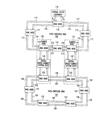
FIG. 1 shows) in simplified form, path-switched ring transmission
system 100 interworking with another path-switched ring transmission system
101.
In this example, path-switched ring 100 includes ring nodes 110 through 115,
and
the other path-switched ring 101 includes ring nodes 120 through 125. Ring
nodes
112 and 120 form first shared node 130 for interworking communications
circuits
between path-switched ring 100 and path-switched ring 101. Similarly, ring
nodes
.,~ji~
-~ ~~ ~ .~t v i!
-4-
114 and 125 form an additional shared node 131 for interworking communications
circuits between path-switched ring 100 and path-switched ring 101. In this
example, ring nodes 112 and 120 in shared node 130 are shown as being
interconnected by inter-ring grooming apparatus, namely, digital cross-connect
system (DCS) 132. Similarly, ring nodes 114 and 125 in shared node 131 are
shown
as being interconnected by inter-ring grooming apparatus, namely) digital
cross-
connect system (DCS) 133. Both DCS 132 and DCS 133 are so-called wide-band
cross-connect systems of a type known in the art and described in the
Technical
Reference entitled "Wideband and Broadband Digital Cross-Connect Systems
Generic Requirements and Objectives", TR-TSY-000233, Issue 2, September 1989,
Bell Communications Research. It will be apparent that other wide-band
grooming
apparatus may be equally employed to realize the inter-ring grooming of
communications circuits. One other such inter-ring grooming apparatus is a
wide
band digital multiplex system) for example) the DDM-2000 Multiplex System
available from AT&T Company.
Ring nodes 110 through 115 are interconnected by transmission path
116 in a counter-clockwise direction and by transmission path 117 in a
clockwise
direction to form path-switched ring 100. In this example, transmission paths
116
and 117 are comprised of optical fibers and) typically, each is comprised of a
single
optical fiber. Such path-switched ring transmission systems are known.
Similarly,
ring nodes 120 through 125 are interconnected by transmission path 128 and by
transmission path 129 to form path-switched ring 101. In this example,
transmission
of digital signals in the SONET digital signal format is assumed. However, it
will be
apparent that the invention is equally applicable to other digital signal
formats, for
example, the CCITT synchronous digital hierarchy (SDH) digital signal formats.
In
this example) it is assumed that an optical OC-N SONET digital signal format
is
being utilized for transmission over transmission paths 116 and 117 in path-
switched
ring 100 and a similar or some other digital signal over transmission path 128
in
path-switched ring 101. The SONET digital signal formats are described in a
Technical Advisory entitled "Synchronous Optical Network (SONET) Transport
Systems: Common Generic Criteria", TA-NWT-000253, Bell Communications
Research) Issue 6, September 1990.
For purposes of this description, a "communications circuit" is
considered to be a SONET STS-3 digital signal having its entry and exit points
on
the particular ring. However, for brevity and clarity of exposition, the inter-
ring
grooming will be described using STS-1 SONET signals as the higher level
signals
-5-
and VT SONET signals as the lower level signals. Again, other digital signal
formats may be equally employed. Another example of such digital signal
formats
are the known DS3 and DS 1 digital signals. Additionally) the SDH STM and SDH
VC lower order digital signal formats maybe equally employed.
S Each of ring nodes 110 through 115 and 120 through 125 comprises an
add-drop multiplexer (ADM). Such add-drop multiplexer arrangements are known.
For generic requirements of a SONET based ADM see the Technical Reference
entitled "SONET ADD-DROP Multiplex Equipment (SONET ADM) GENERIC
CRITERIA", 'rR-TSY-000496, Issue 2, September 1989, Supplement 1, September
1991, Bell Communications Research. In this example, the ADM operates to pass
signals through the ring node) to add signals at the ring node and to drop
signals at
the ring node.
FIG. 2 shows, in simplified block diagram form, details of ring nodes
110 through 115 and ring nodes 120 through 125. In this example, a west (W)-to-
east (E) digital signal transmission direction is assumed in the bandwidth on
transmission path 116. It will be apparent that operation of the ring node and
the
ADM therein would be similar for an east (E) - to - west (Vii digital signal
transmission direction in the bandwidth on transmission path 117.
Specifically,
shown is transmission path 116 entering the ring node and supplying an OC-N
SONET optical signal to receiver 201, where N could be, for example, 3, 12 or
48.
Receiver 201 includes an optical/electrical (O/E) interface 202 and a
demultiplexer
(DEMUX) 203, which yields at least one (1) STS-M SONET digital signal. Such
O/E interfaces and demultiplexers are known. In this example, M is assumed to
be
three (3) and N is greater than M. The STS-M signal output from DEMUX 203 is
supplied to broadcast element 206. A broadcast element replicates the STS-M
signal
supplied to it and supplies the replicated signals as a plurality of
individual outputs.
Such broadcast elements are known. Broadcast element 206 generates two
identical
STS-M signals and supplies one STS-M signal to an input of 2:1 selector 207
and
another STS-M signal to an input of 2:1 selector 208. An STS-M signal output
from
2:1 selector 207 is supplied to transmitter 211 and, therein, to multiplexer
(MUX)
212. The output of MUX 212 is an electrical OC-N digital signal, which is
interfaced to transmission path 116 via electrical/optical (E/O) interface
213. Such
multiplexers (MUXs) and electrical/optical (E/O) interfaces are well known.
Similarly, in the east (E) - to - west (V~ direction an OC-N optical
signal is supplied via transmission path 117 to receiver 214 and, therein, to
optical/electrical (O/E) interface 21 S. In turn, demultiplexer (DEMUX) 216
yields a
.: .. , ; ,.; ~ , ..
,.: ' . .
:;~ .
>
-
:
w
'
~
: ; . .
. .. ~ .,
.' ,
: .
,
: . ..
. ;~... ~:_:
. . ,
~~, , :
yy ; ~-. .. . .;.~.; .. :.. ; ., ,, s;,., ,,
: ;.
.
;. ; :. , . ,: ;; :; . .: ;. ,:.. .. ,
. , ~. ~ . , .. .
:; . ; : .
' ;,' ; ' '
~
. ...
.
.
,. ~,.. '~r~ , . ;
t.~ ~ J i~ :l iI
-6-
S'TS-M signal which is supplied to broadcast element 218. Broadcast element
218
replicates the STS-M signal into a plurality of identical STS-M signals, in
this
example, three (3). One STS-M signal is supplied to an input of 2:1 selector
208) a
second STS-M signal is supplied to an input of 2:1 selector 209 and a third
STS-M
signal is supplied to interface 231. An output from 2:1 selector 209 is
supplied to
transmitter 220. In transmitter 220, multiplexer (MUX) 229 multiplexes the STS-
M
into an electrical OC-N and, then, electrical/optical (E/O) interface 222
supplies the
optical OC-N signal to transmission path 117.
Thus, in this example) broadcast element 218 supplies the secondary
communications circuits from the additional shared node as candidates for
through
circuits and also drops the secondary communications circuits via interface
231
under control of controller 205. It should be noted that although the
communications
circuits are SONET STS-3 digital signals, interface 231 and interface 224 drop
SONET STS-1 digital signals. Similarly, STS-1 digital signals are combined in
the
interfaces to form STS-3 digital signals, in known fashion. Additionally, it
is noted
that selector 208 selects on a STS-1 level. To this end, the STS-3 digital
signals are
demultiplexed in selector 208 to obtain the three STS-1 digital signals, the
STS-1
signals are selected and then multiplexed back into a STS-3 signal, which is
supplied
to interface 224. Selector 209 is provisioned under control of controller 205
to
normally select the STS-M signal being supplied from interface 224.
Controller 205 operates to control selection of the STS-3 signals via
selectors 207) 208 and 209 based on their health. Controller 205 communicates
with
demultiplexers 203 and 216 and multiplexers 212 and 221 via bus 223, with
interface 224 via bus 227) with interface 231 via bus 232) with selector 207
via bus
234, with selector 209 via bus 225 and with selector 208 via bus 235.
Specifically,
controller 205 monitors the incoming digital signals to determine loss-of
signal)
alarm conditions) presence of alarm indication signal (AIS) and the like. When
operating as a primary interworking ring node) controller 205 controls the
dropping,
via interface 231, of the secondary communications circuits being supplied
from the
secondary ring node of shared node 131 (FIG. 1 ) and the dual feeding on an
STS-M
signal from interface 224 via broadcast element 226 and selectors 207 and 209.
When operating as a secondary interworking ring node, controller 205 controls
the
revertive biasing of selector 207 to normally select the STS-M signal from
broadcast
element 206, i.e., from the primary interworking ring node to be supplied as
an
output on transmission path 116. If) however, there is a failure in the
primary
interworking ring node, controller 205 controls selector 207 to select the
secondary
F.~
communications circuit (STS-M) being supplied from interface 224 via broadcast
element 226. When the failure in the primary interworking ring node has been
repaired or the STS-M signal otherwise becomes healthy again, selector 207
automatically reverts back to selecting it under control of controller 205. To
this
end, the health of the communications circuit TP from the primary node and the
communications circuit Ts in the secondary node is monitored to determine if
selector 207 will make a real time switch to select Ts. It is the dual feed of
TP in
the primary node and the revertive real time selection via selector 207 in the
secondary node that eliminated the need to also evaluate and select low level
signals
derived from the high level signal being groomed in the secondary node and
from a
corresponding communications circuit supplied from the primary node which will
be
combined to form a "new" communications circuit for transmission. It should be
noted) however, that there is rarely a need for selector 207 to select Ts; it
is done
only under duress.
Interface 224 is employed to interface, in this example, to the particular
inter-ring grooming apparatus being employed. As indicated above, in this
example
both interface 224 and interface 231 between STS-3 digital signals to STS-1
digital
signals, in known fashion. Specifically, an STS-3 digital signal to be dropped
at the
ring node is supplied to interface 224 via 2:1 selector 208, under control of
controller
205, from either broadcast element 206 or broadcast ele~nt 218. When operating
as a primary interworking ring node) selector 208 normally is controlled to
select the
STS-3 signal being supplied from the west (V~ via broadcast element 206 and
when
operating as a secondary interworking ring node selector 208 is controlled to
select
the STS-3 signal being supplied from the east (E) via broadcast element 218.
This
STS-3 signal is demultiplexed in interface 224 and supplied as three (3) STS-1
signals (R) to circuit path 230. Similarly, in the primary interworking ring
node, an
STS-3 secondary communications circuit being supplied, via broadcast element
218,
to interface 231 is demultiplexed therein, under control of controller 205,
and
supplied as three (3) STS-1 signals (R') to circuit path 233. A signal ('I~ to
be added
at the ring node is supplied to interface 224 where it is converted to the STS-
M
digital signal format, if necessary. The STS-M digital signal is then supplied
to
broadcast element 226 where it is replicated. The replicated STS-M digital
signals
are supplied by broadcast element 226 to an input of 2:1 selector 207 and an
input of
2:1 selector 209. In this example) 2:1 selectors 207 and 209, under control of
controller 205, dual feed the signal being added for transmission in the
bandwidth on
both transmission path 116 and transmission path 117.
:-j ~~ .~~ : ;
~. ~, ::~ U a i t~
_g_
In summary, the provisioning of primary ring node 112 and secondary
ring node 114 to realize the invention is as follows:
At primary ring node 112
disable path switching in selector 208 for communications circuit TA
incoming from the west from termination ring node 110;
select drop port for communications circuit TA;
select drop port for communications circuit TS from secondary node
114 (note communications circuit T A and communications circuit T s occupy the
same txibutary to the east and west and if the normal path switching was
applied it
would be selecting between Tb and Ts;
At secondary ring node 114
disable path switching in selector 208 for communications circuit T A
incoming from the east from termination ring node 110;
enable monitor on selector 208;
enable revertive switching of selector 208 with initial condition being
through.
Additionally, the provisioning at termination ring node 110 is as
follows:
Provision communications circuit to drop; For the drop, the following
normal path switching functions apply:
Communications circuit TA is dual fed on the same tributary to the east
and the west;
Receive communications circuit is selected based on path criteria, i.e.,
health of the path, from the east or west.
Controller 205 controls and monitors the status of interface 224 and the
digital signals being supplied thereto via bus 227 and controls and monitors
interface
231 via bus 232. Specifically, controller 205 monitors interface 224 for loss-
of
signal, coding violations and the like.
FIG. 3 shows, in simplified block diagram form, a digital cross-connect
system (DCS) including apparatus embodying an aspect of the invention. It is
noted
that for brevity and clarity of description only one direction of signal
transmission is
shown and only one digital signal will be considered. It will be apparent to
those
skilled in the art that there is a similar opposite direction of transmission
and that a
relatively large number of digital signals would normally be groomed by such a
F; ~ J ~,< i~ !
-9-
DCS. Again, in this example) a SONET STS-1 digital signal is being groomed at
the
lower VT digital signal level. Specifically, shown is an STS-1 signal (T')
being
supplied from ring node 120 (FIG. 1) in path-switched ring 101 to DCS 132 and
therein to demultiplexer (DEMUR) 301. DENIUX 301 demultiplexes the STS-1
signal to obtain the VT signals in known fashion. The VT signals are supplied
to
time slot interchanger (TSI) 302 where they are groomed under control of
controller
303. Then) the groomed VT signals are supplied on a one-to-one basis to 2:1
selectors 304-1 through 304-Y) where Y is the number of VT signals being
transported by the STS-1 signal. Similarly) a corresponding inter-ring groomed
STS-1 signal (R') supplied from secondary interworking ring node 114 in shared
node 131 is demultiplexed in demultiplexer (DEMUR) 305 to obtain VT signals
which correspond on a one-to-one basis with the VT signals being supplied to
selectors 304 from TSI 302. The VT signals from DEMUR 305 are supplied on a
one-to-one basis to other inputs of selectors 305-1 through 305-Y. Controller
303
evaluates the VT signals on a pair-wise basis) in this example, in both DEMUR
301
and DEMUR 305, to determine the best VT signal in each pair and, then, causes
selectors 304 to select the best VT signals. The evaluation may include
monitoring
the VT signals for loss of signal, AIS and/or bit error rate. The selection of
the VT
signals is such that the corrupted and/or failed VT signals are not selected.
Thereafter, the selected VT signals are combined via multiplexer (MUX) 306 to
obtain the desired inter-ring groomed STS-1 signal ('17.
FIG. 4 shows) in simplified block diagram form another arrangement
embodying an aspect of the invention. Specifically) shown are DCS 401 and
selector
unit 402 which form inter-ring grooming apparatus 132. It is noted that for
brevity
and clarity of description only one direction of signal transmission is shown
and only
one digital signal will be considered. It will be apparent to those skilled in
the art
that there is a similar opposite direction of transmission and that a
relatively large
number of digital signals would normally be groomed by such a DCS. Again, in
this
example, a SONET STS-1 digital signal is being groomed at the lower VT digital
signal level. DCS 401 includes controller 403, DEMUR 404) TSI 405 and MUX 406
and operates in known fashion to groom STS-1 signals at the VT signal level.
Specifically, shown is an STS-1 signal (T') being supplied from ring node 120
(FIG.
1 ) in path-switched ring 101 to DCS 401 and therein to DEMUR 404. DEMUR 404
demultiplexes the STS-1 signal to obtain the VT signals in known fashion. The
VT
signals are supplied to TSI 405 where they are groomed under control of
controller
403. Then, the groomed VT signals are supplied to MUX 406 where they are
~: _i. ~1 V l~ t ~.~
- 10-
combined into a groomed STS-1 signal ( T~~ ). The groomed STS-1 signal T~~ is
supplied to selector unit 402 and therein to DEMUR 407. DEMUR 407
demultiplexes the groomed STS-1 signal T~~ to obtain the VT signals. The, the
VT
signals are supplied on a one-to-one basis to first inputs of 2:1 selectors
408-1
through 408-Y, where Y is the number of VT signals being transported by the
STS-1
signal. Similarly, a corresponding inter-ring groomed STS-1 signal (R')
supplied
from secondary interworking ring node 114 in shared node 131 is demultiplexed
in
DEMUR 409 to obtain VT signals which correspond on a one-to-one basis with the
VT signals being supplied to selectors 408 from DEMUR 407. The VT signals from
DEMUR 409 are supplied on a one-to-one basis to second inputs of selectors 408-
1
through 408-Y. Controller 410 evaluates the VT signals on a pair-wise basis,
in this
example, in both DEMUR 407 and DEMUR 409) to determine the best VT signal in
each pair and) then, causes selectors 408 to select the best VT signals. The
evaluation may include monitoring the VT signals for loss of such coding
errors and
the like. The selection of the VT signals is such that the corrupted andfor
failed VT
signals are not selected. Thereafter, the selected VT signals are combined via
MUX
411 to obtain the desired inter-ring groomed STS-1 signal (T).
FIG. 5 illustrates in flow chart form the operation in secondary ring node
114 of selector 207 (FTG. 2) in effecting the revertive selection between new
primary
communications circuit Tp from primary ring node 112 and secondary
communications circuit T S from ring node 114. The operation is entered vi
step
501. Then, step 502 causes the health to be obversed of signals Tp and Ts.
Step
503 tests to determine if signal Tp fails the comparison criteria with Ts. If
the test
result is NO, Tp is normal, and control is returned to step 502 and steps 502
and 503
are iterated. If the test result in step 503 is YES, Tp is abnormal, and step
504
causes a switch to signal T s . Then, step 505 causes the health to be
observed of
signals Tp and TS. Step 506 tests to determine if signal Tp passes the
comparison
criteria with T S . If the test result is NO, T p continues to be abnormal,
and control is
returned to step 505 and steps 505 and 506 are iterated. If the test result in
step 506
is YES) Tp has returned to normal, and step 507 causes a switch, i.e., an
automatic
reversion, to signal Tp and control is returned to step 502. Thereafter, the
process is
repeated.
FIG. 6 illustrates in simplified form a "normal" ring interworking
communications circuit connection in path-switched ring 100. Specifically) the
communications circuit connection is between ring node 110, the A termination,
and
its primary interworking ring node 112 and its secondary interworking node
114.
y ? :',~. ;o -_, 1 ~
' ~
F.~ .L ;i u' '~ V
-11-
Thus, one portion (Tp) of the duplex communications circuit enters ring 100 at
ring
node 110 and is supplied in the bandwidth of transmission path 116 through
ring
node 111 to its primary interworking ring node 112 and is supplied in the
bandwidth
of transmission path 117 through ring node 115 to its secondary interworking
ring
node 114. The transmit portion, i.e.) TA of the communications circuit is
normally
handed-off as Rp in ring node 112 and as RS in ring node 114. Similarly,
another
portion (Tp) of the duplex communications circuit normally enters ring 100 at
its
primary interworking ring node 112 and is supplied to the bandwidth of
transmission
path 117 and to the bandwidth of transmission path 116. Tp is supplied in
transmission path 116 via ring node 113 to secondary interworking ring node
114.
in ring node 114 Tp is normally selected and supplied through ring node 115 to
ring
node 110 where it is also received as RA. In transmission path 117, this
portion of
the connmunications circuit is passed through ring node 111 and received as R
A at
ring node 110. Ring node 110 normally selects R A from transmission path 117.
Additionally) this portion of the communications circuit is supplied as Ts
from
secondary interworking ring node 114 in the bandwidth of transmission path 117
through ring node 113 and is dropped at primary ring node 112 as
unidirectional
communications circuit R~" . Then communications circuit R~P is available so
that
the lower level digital signals may be obtained for comparison and selection.
Secondary interworking ring node 114
FIG. 7 illustrates the ring interworking communications circuit
transmission in ring 100 when a failure arises in the hand-off link in its
primary
interworking node 112. As indicated above) when a portion of the hand-off link
fails, for example, the transmit portion T p, the same "good" transmit signal
T s is
selected in secondary interworking ring node 114 and supplied in the bandwidth
on
transmission path 116 to ring node 110. Ring node 110 selects the transmit
signal
T$ from transmission path 116 as receive signal RA. Primary interworking ring
node 112 can still select the received portion (Rp) of the communications
circuit
from ring node 110. However, if the received portion of the hand-off link has
failed,
secondary interworking ring node 114 selects the received signal (R S ), which
is
being supplied on transmission path 117 from ring node 110.
The above-described arrangements are) of course, merely illustrative of
the application of the principles of the invention. Other arrangements may be
devised by those skilled in the art without departing from the spirit or scope
of the
invention. It will be apparent that evaluation and selection of the lower
level digital
signals from the primary inter-ring groomed communications circuits and the
. . : : . '. , ...:.:
. : ; : . ~'
. . . . .
y ( ,; : . . ... . .. :; . ' ... . . . .~~:
.
;1 7"~
l 1
;:~~JJ t t~
-12-
secondary inter-ring groomed communications circuits could also be included in
the
primary ring nodes.
i: ,