Note: Descriptions are shown in the official language in which they were submitted.
WO 94/15401 PCT/US93112693
2i3o2ss
DIGITALLY CONTROLLED PHASE SHIFTER
Field of Invention
The present invention relates generally to signal
controlled phase shifters and more particularly to a
phase shifter including at least several delay elements
having connections to an outaut terminal controlled in
response to the value of a control signal.
The invention is also related to a signal
multiplexer =esponsive to at least several signals and
more partic::larly to such a multiplexer which is
responsive to a reflected coded signal.
. BackcTround Ar t
Signal controlled phase shifters are usually
analog devices including a variable reactance, such as
a varactor, :zaving a value controlled by the amplitude
.5 of a voltage. Such phase shifters are frequently
employed in voltage controlled variable frequency
oscillators, such as are employed in phase locked
loops. In such applications, a fixed clock is supplied
to the voltage controlled, variable frequency
oscillator to derive an output frequency that is fed
back to one input of a phase detector, having a second
input responsive to an input frequency. The phase
detector derives an error voltage that is fed to a loop
filter which supplies the voltage controlled oscillator
with a variable amplitude voltage for controlling the
oscillator output freQUency. Phase locked loops are
~'~~:~~~~s~~
~O 94/15401 PCT/US93I12693
21.30268
used to lock a receiver to an incoming frequency with
zero frequency or phase error. In receivers responsive ,
to variable phase signals representing digital data,
e.g. QPSK or BPSK signals, a demodulator of the
receiver is locked to a symbol frequency with zero
phase error. Such locking is usually performed with a
first or second order phase locked loop.
The prior art analog phase shifters and analog
based phase locked loops have the usual disadvantages
associated with analog circuitry, i.e., lack of
repetitiveness in manufacturing and performance unless
"tweaking" procedures are used, low yield production,
inaccuracy and the need to adapt the analog circuitry
to the remaining parts of the equipment.' To overcome
these problems, digitally based phase locked loops have
been developed. One digitally based phase locked loop
responsive to base band signals to be demodulated
includes an analog-to-digital converter having one
input responsive to such a signal. The converter has a
second input responsive to a sampling clock having a
variable frequency controlled by the digital phase
locked loop. The converter derives a multi-bit digital
output signal having a variable value dependent on the
amplitude of the base band signal when a sample derived
by the clock occurs. The base band signal is subject
to a full gamut of amplitude variations because of
imperfections in the transmission and processing of the
signal between the origination site and the phase
locked loop site. Normally at least two samples of the
variable phase signal are taken during each symbol.
The variable digital output signal of the
converter is supplied to a symbol data decoder and
error generator. The symbol data decoder and error
generator derives a data output signal representing the
WO 94/15401 PCTIUS93I12693
-...
3
2130268
digital value of the symbol, as well as a signal
indicative of the phase error between the variable
phase signal and the sampling clock. The phase error
digital control signal is supplied to a symbol timing
loop filter, which in turn drives a direct digital
synthesizer, having a digital output signal with values
representing the amplitude of a sine wave. The direct
digital synthesizer drives a digital to analog
converter, having a sinusoidal-like output with values
equal to the digital values derived by the synthesizer.
The digital to analog converter sinusoidal-like output
is supplied to a lowpass filter. Direct digital
synthesizers are frequency limited to a few megaHertz,
so the lowpass filter output is considerably lower in
frequency than the base band signal supplied to the
analog-to-digital converter. To provide the analog-to-
digital converter with an acceptable sampling
frequency, the lowpass filter output is supplied to a
frequency multiplying phase locked loop. Hence, this
prior art system is relatively complex, requiring an
analog phase locked loop within the digital phase
locked loop, as well as a digital to analog converter
and a lowpass filter.
Another prior art digitally based system for
demodulating variable phase intelligence signals
supplied to a receiver includes an analog-to-digital
converter having first and second inputs respectively
responsive to the base band signal and a fixed
frequency sampling clock. The analog-to-digital
converter derives a digital output having values
indicative of the amplitude of the base band signal
supplied to the converter at the time each sampling
clock occurs. To determine the precise level of the
analog-to-digital converter output signal, an
Z. ~ i.j'~.>" '~..3 y ~'srat'~
WO 94!15401 PCTIUS93112693
4
4268
4. x1
interpolator responds to the converter output to find
the sampled values at the desired time. The
interpolator is either of the finite or infinite
impulse response type. The interpolator derives a
digital output which is supplied to a symbol timing
processor having an output which updates coefficients
used in the interpolator. The symbol timing processor
also derives data representing output signals.
One further type of digitally based phase locked
loop samples the amplitude of a received signal. The
resulting samples are processed to derive an error
control signal for the frequency of the sampling
source. The error control signal controls the
frequency of the sampling source by selecting one of
several predetermined frequency division factors for a
fixed clock source. As the error changes, the
frequency division factor changes, to vary the sampling
source frequency by discrete, fixed amounts. This type
of phase lock loop has the disadvantage of not being
suitable for high frequency sampling sources and does
not provide high frequency resolution.
It is, accordingly, an object of the present
invention to provide a new and improved signal
controlled phase shifting apparatus and method.
Another object of the present invention is to
provide a new and improved signal controlled variable
frequency oscillator and to provide a method of
deriving a variable frequency wave in response to a
control signal.
An additional object of the invention is to
provide a new and improved digitally based phase locked
loop and a method of digitally phase locking an input
frequency and a clock.
Still another object of the invention is to
o
t
...". '
x130268
provide a digitally based phase locked loop including a
digitally controlled asynchronous phase shifter
responsive to a fixed frequency clock.
A further object of the present invention is to
5 provide a digitally based phase locked loop suitable
for high frequencies that is relatively inexpensive
because it employs a fixed frequency oscillator
reference.
The Invention
In accordance with one aspect of the invention, a
method of changing a clock wave having a predetermined
fixed frequency to derive an output wave comprises
deriving a digital control signal having a value that
varies in response to the relative phase of a constant
frequency input signal and the output wave, subjecting
the clock wave to at least several discrete delays so
there are derived at least several waves having differing
time positions that are replicas of the clock wave,
selecting one of the at least several waves having
differing time positions in response to the value of the
digital control signal to derive the output wave, and
resetting the value of the digital control signal to a
predetermined initial value therefor each time the output
wave changes phase relative to the clock wave by
approximately 360° due to a lead/lag change in the phase
relationship of the output wave and clock wave.
The invention also is directed to a method of
discretely changing a phase delay of a clock wave as a
function of time, possibly by amounts in excess of
multiples of 360°, by converting the value of a desired
phase delay for the clock wave into a signal having at
least several discrete values that change as a function
of time, incrementing the discrete value of the signal at
a certain rate for every unit of desired phase delay
change in a cycle of the clock wave, establishing at
~,~:~.r~
a~ 302 sa
6
least several discrete delay times for the clock wave,
selecting one of the at least several discrete delay
times for the clock wave in response to the discrete
value of the signal so there is a correspondence between
the discrete delay times to which the clock wave is
subjected and the changing values of the discrete signal,
delaying the clock wave by the selected discrete delay
time to derive a delay subjected clock wave, and
resetting the discrete value of the signal to a
predetermined value in response to the phase of the delay
subjected clock wave changing over approximately an
integral multiple of 360° of the phase of the clock wave.
The methods are performed to attain a phase lock
between a constant frequency input and the clock wave,
wherein the discrete delay is attained by: sampling the
amplitude of the input at a sampling frequency determined
by the selected clock wave, responding to the sampled
amplitude to derive a first representation having a value
equal to the frequency error between the sampling
frequency and the constant frequency input, shifting the
frequency of the clock wave by an amount determined by
the value of the first representation by integrating the
first representation to derive a second representation
having a value commensurate with a phase shift to be
imposed on the clock wave, the phase shift to be imposed
having one of at least several different discrete values.
The input may include data symbols, in which case
the sampling is performed at least once per symbol to
derive for each symbol a multi-bit digital representation
of the sampled amplitude. Preferably, the discrete value
is reflected coded and the discrete value is reset to
zero. The aforementioned methods can be performed by
appropriate apparatus and means.
According to another aspect, apparatus for shifting
a phase delay of a clock wave in response to a control
signal representing a phase change to be applied to the
;1302 68
clock wave comprises a circuit responsive to the clock
wave for deriving at least several replicas of the clock
wave, wherein the replicas have differing time delays
with respect to each other. A coupler responsive to the
phase change representing signal couples a selected one
of the replicas to an output terminal as a function of
the value of the control signal. The apparatus is
included in a phase locked loop including an analog-to-
digital converter responsive to symbols to be sampled by
the converter. At least a portion of the symbols have a
tendency to be degraded. The converter derives a multi-
bit digital signal representing the amplitude of one of
the symbols in response to a sampling wave train derived
in response to the selected replica at the output
terminal. A signal deriver responsive to the converter
derives signals representing the frequency error and
phase correction of the symbols as applied to the
converter relative to the selected replica and the
derived phase correction signal is the control signal.
Preferably, the signal deriver integrates the
frequency error representing signal derived from the
converter to derive a signal representing the integrated
frequency error derived from the converter. The signal
deriver also preferably includes a counter responsive to
the signal representing the integrated frequency error
derived from the converter for deriving the phase
correction signal. The counter is reset to zero in
response to detection of the selected replica at the
output terminal being shifted through an integral
multiple of one cycle of the clock.
The counter preferably derives a reflected coded
control signal having M bits for controlling the coupler
and the replica is derived by a circuit including a
multiplexer having N signal input terminals designated 0,
1. 2...(N-1) respectively responsive to replicas of the
clock having delay times of approximately 0, DT,
~~ '~.,,a.. ~°,,-~ .!'G'.. A'i_T
~~! ~'.s..J"u" °Jrt.ib~.J.~d..~
21 302 68 _
8
2DT....(N-1)DT, where DT is a unit delay time. The
multiplexes includes (N-1) gates each having: (a) first
and second signal inputs, (b) a signal output and (c) a
control input responsive to a bit of the reflected coded
signal for routing the signal at one of the two signal
inputs to the signal output as a function of the bit
value at the control input . The signal inputs and signal
outputs of the gates are connected to each other. The
multiplexes input terminals and the multiplexes output
terminal and the control inputs of the gates are
connected to be responsive to the M bits of the control
signal so that, as the reflected signal value changes
from a reflected value representing the value in base 10
of i to (i+1), the signal at the multiplexes output
terminal changes from the signal at multiplexes input
terminal i to the signal at multiplexes input terminal
(i+1), where i is selectively each of 0, 1, 2...(N-2).
Another aspect of the invention concerns an
apparatus for shifting a phase delay of a clock wave in
response to a control signal representing a phase change
to be applied to the clock wave. The apparatus comprises
a circuit responsive to the clock wave for deriving at
least several replicas of the clock wave wherein the
replicas have differing time delays with respect to each
other. A coupler responsive to the phase change
representing signal couples a selected one of the
replicas to an output terminal as a function of the value
of the control signal. The replica deriving means
includes (N-1) cascaded substantially equal time delay
elements designated 1, 2...(N-1) and includes a
multiplexes having N input terminals designated 0, 1,
2...(N-1), wherein input terminal 0 is responsive to the
clock and input terminal k is responsive to the replica
derived from delay element k and k is selectively each of
1, 2...(N-1). The multiplexes includes another input
responsive to the control signal and the output terminal,
"~,.,,..
21 30268
9
the phase change signal being reflected coded. The
multiplexes includes an array of (N-1) gates each having:
first and second signal inputs, a signal output and a
control input responsive to a bit of the reflected coded
signal for routing the signal at one of the two signal
inputs to the signal output as a function of the bit
value at the control input.
Another aspect of the invention concerns an
apparatus for shifting a phase delay of a clock wave in
response to a control signal representing a phase change
to be applied to the clock wave. The apparatus comprises
a circuit responsive to the clock wave for deriving at
least several replicas of the clock wave, wherein the
replicas have differing time delays with respect to each
other. A coupler responsive to the phase change
representing signal couples a selected one of the
replicas to an output terminal as a function of the value
of the control signal. The apparatus is included in a
variable frequency oscillator responsive to a frequency
control signal. An integrator responsive to the
frequency control signal derives the phase change
representing signal.
The apparatus for shifting a phase delay of a clock
wave in response to a control signal representing a phase
change to be applied to the clock wave can also be
considered to comprise a circuit responsive to the clock
wave for deriving at least several replicas of the clock
wave wherein the replicas have differing time delays with
respect to each other. A coupler responsive to the phase
change representing signal couples a selected one of the
replicas to an output terminal as a function of the value
of the control signal. The coupler includes a
multiplexes having a signal output terminal, as well as
N signal input terminals designated by 0, 1, 2...(N-1).
The multiplexes is responsive to a reflected coded signal
having M bits where 2M - N and N is an integer greater
21 30268 _
to
than 2. The multiplexes includes: (N-1) gates each
having first and second signal inputs, a signal output
and a control input responsive to a bit of the reflected
coded signal for routing the signal at one of the two
signal inputs to the signal output as a function of the
bit value at the control input. The signal inputs,
signal outputs, signal input terminals and control inputs
and the M bits are coupled together so that, as the
reflected signal value changes from a reflected value
representing the value in base 10 of i to (i+1), the
signal at the output terminal changes from the signal at
input terminal i to the signal at input terminal (i+1),
where i is selectively each of 0, 1, 2...(N-2).
The coupler when switched in response to the phase
change control signal has a tendency to derive a glitch
at the output terminal. Preferably, a circuit coupled to
the output terminal prevents the coupling of the glitches
to the output terminal.
A further aspect of the invention relates to a
method of attaining phase lock between a constant
frequency input and a clock wave having a frequency
slightly different from the constant frequency by
sampling the amplitude of the input at a sampling
frequency, responding to the sampled amplitude to derive
a first representation having a value equal to the
frequency error between the sampling frequency and the
constant frequency input and shifting the frequency of
the clock wave by an amount determined by the value of
the first representation by integrating the first
representation to derive a second representation having
a value commensurate with a phase shift to be imposed on
the clock wave. The phase shift to be imposed has one rf
at least several different discrete values. Adjacent
ones of said phase shift values are approximately equally
spaced from each other. A delay is imposed on the clock
~f
21 30268
wave for a time directly proportional to the selected
discrete value to derive the frequency shifted clock.
A further aspect of the invention relates to a
method of discretely changing a phase delay of a clock
wave as a function of time by deriving a signal having at
least several discrete changing values as a function of
time, establishing at least several discrete delay times
for the clock wave, responding to at least several of the
values of the signal to subject the clock wave to at
least several of the established discrete delay times so
there is a correspondence between the discrete delay
times to which the clock wave is subjected and the
changing values of the signal so the clock wave as
subjected to the delays is discretely phase shifted and
establishing the at least several discrete delay times by
applying the clock to at least several cascaded delay
units having discrete delay times. The responding step
is performed by changing the number of the cascaded delay
units connected to the clock wave so that as the signal
value changes, the cascaded delay units are connected to
and disconnected from the clock wave.
An added aspect of the invention concerns an
apparatus for shifting the phase of a periodic waveform
in response to the value of a control signal, wherein the
phase shift is interposed between an output terminal of
a source of the waveform and another output terminal.
The apparatus comprises at least several delay units
having discrete delay times and a controller responsive
to the value of the control signal. The controller
controls connections of the delay units between the
waveform source output terminal and the another autput
terminal so that as the value of the control signal
changes there are corresponding changes in the delay time
interposed by the delay units on the periodic waveform
between the waveform source output terminal and the
another output terminal. The delay units are cascaded
X130268
12
with each other and the controller responds to the value
of the control signal for effectively controlling the
number of the delay units cascaded between the source
output terminal and the another output terminal so that
as the value of the control signal changes there are
corresponding changes in the number of the delay units
effectively cascaded between the output terminals. 1,
2...N of said delay units are provided such that delay
unit 1 is connected so an output thereof is connected to
said another output terminal without connections through
any other of said N delay elements. The controller
controls connections between input and output terminals
of the delay units and between the source output terminal
and the input terminal of said delay unit 1 so that in
response to the control signal having a value commanding
k of said delay units to be cascaded between the source
output terminal and the another output terminal the input
terminal of delay unit k is connected to the source
output terminal without connections through any other of
said N delay elements . The output terminal of delay unit
j is connected to the input terminal of delay unit ( j-1 ) ,
where k is selectively any integer between 2 and N and j
is selectively every integer between 2 and k.
The controller preferably establishes the connection
between delay units k and (k-1) before breaking the
connection between an input of delay unit (k-1) and the
waveform source output terminal in response to the
interposed delay changing from k to (k-1).
The invention also relates to an apparatus for
shifting the phase of a periodic waveform in response to
the value of a control signal wherein the phase shift is
interposed between an output terminal of a source of the
waveform and another output terminal. The apparatus
comprises at least several delay units having discrete
delay times and a controller responsive to the value of
the control signal. The controller controls connections
a '~~~A~-~~t3~TR,CE
X130268
13
of the delay units between the waveform source output
terminal and the another output terminal so that as the
value of the control signal changes there are
corresponding changes in the delay time interposed by the
delay units on the periodic waveform between the waveform
source output terminal and the another output terminal,
N of said delay units are provided so there is a
possibility of N different discrete time delays. The
controller responds to the value of the control signal to
selectively connect k of said N delay elements in
cascaded relation with each other between the waveform
source output terminal and the another output terminal
while decoupling the remaining (N-k) delay units from the
k cascaded delay units.
In a preferred embodiment, the controller divides
the N elements into plural groups and monotonically
changes the value of k from (1) 1 to P for a first group
of P of the N elements during a first time interval, and
( 2 ) then from 1 to Q for a second group of Q of the
elements during a second time interval.
The controller preferably includes a counter having
P states that are sequenced from 1 to P. A coupler
couples control signals indicative of (1) which of the P
states the counter is in from the counter to the first
group of P elements during the first time interval and
(2) which of the Q states the counter is in from the
counter to the second group of Q elements during the
second time interval, where Q is no greater than P.
r a°t v
~~3o2ss
14~
Accordingly, still a further object of the
invention is to provide a new and improved signal
multiplexes having at least several input terminals and
Which is responsive to a reflected coded signal for
coupling the signal at one of the terminals to an
output terminal. .
' An added object of the invention is to provide a
signal multiplexes having at least several input
terminals and which is responsive to a reflected coded
signal so that there is a one-to-one relationship
between the base 10 values of the reflected coded
signals and the signal at the selected input terminal
which is coupled to the output terminal.
The above and still further objects, features and
advantages of the present invention will become
apparent upon consideration of the following detailed
description of several specific embodiments thereof,
especially when taken in conjunction with the
accompanying drawings.
Brief Description of the Drawing
Fig. 1 is a partial block and partial circuit
diagram of a phase locked loop incorporating a
digitally controlled asynchronous phase shifter in
accordance with one embodiment of the invention;
Fig, 2 is a block diagram of a preferred
embodiment of the multiplexes included in Fig. 1;
Fig. 3 is a block diagram of another embodiment of
,~ ~- _
WO 94/15401 PCT/US93I12693
213o2ss , f : - o. ,
an asynchronous digitally controlled phase shifter in
accordance with the present invention;
Fig. 4 is a schematic diagram of a delay unit
included in the structure illustrated in Fig. 3;
5 Fig. 5 is a circuit diagram of a controller
included in Fig. 3; and
Fig . 6 is a f low diagram of a sequencer included
in Fig. 5.
Description of the Preferred Embodiment
10 Reference is now made to Fig. 1 of the drawing, a
phase locked loop responsive to a receiver base band
quadrature phase shift key signal having I and Q
components on leads 12 and 14, respectively. The
signals on leads 12 and 14 are typically degraded due
15 to the transmitting and receiving processes occurring
prior to derivation of the signals on these leads so
that the original variable phase I and Q channel (bi-
level) amplitudes are transformed into signals having a
gamut of amplitudes between a pair of levels on leads
12 and 14. A typical bit, symbol or baud rate for the
signal on leads 12 and 14 is 20 megaHertz. The signals
on leads 12 and 14 are respectively supplied to analog-
to-digital converters 16 and 18, each of which derives
a multi-bit parallel digital signal having a value
commensurate with the amplitudes of the signal
supplied to the converters at the time the converters
are supplied with a variable frequency sampling clock
via lead 20. In the usual receiver including a phase
locked loop the sampling clock frequency is twice the
Frequency of the symbol rate of the signals on leads 12
and 14 , to provide early and late gate samples , as is
common in the prior art.
The output signals of converters 16 and 18 are
n i i n i i ~ i i i n ~ i
WO 94115401 PCT/US93I12693
2130268
16
supplied to digital data decoder and error generator
22 for deriving parallel multi-bit data and error
outputs on buses 24 and 26, respectively. The error
signal on bus 26 represents (digitally) the deviation
of the sampling phase provided by the signal on lead 20
relative to the ideal sampling point.
The error representing signal on bus 26 is
supplied to symbol timing loop filter 28 for deriving
on bus 30 a parallel mufti-bit digital control signal
representing the frequency error associated with the
error signal on bus 26. Symbol timing loop filter 28
generally derives one frequency error signal for each
symbol on leads 12 and 14. The structure of converters
16 and 18, data decoder and error generator 22 and
symbol timing loop filter 28 is conventional and needs
no further description or explanation.
The frequency error signal derived by symbol
timing loop filter 28 on bus 30 controls the frequency
and phase of the sample clock on lead 20. To this end,
the frequency error signal on bus 30 is converted by
full adder 32, which is effectively a digital
integrator, into a digital phase error signal. The
overflow bit of the phase error signal is supplied to
lead 34 to advance the count in reflected (preferably
Gray) code counter 36, having a reflected code multi-
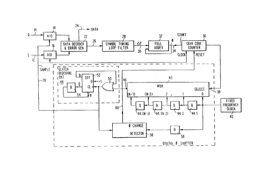
bit parallel output that is supplied to select input 38
of multiplexer 40. Multiplexer 40 includes N signal
input terminals, designated 0,1,2...(N-2) and (N-1).
The N signal input terminals of multiplexer 40 are
responsive to fixed frequency clock source 42 and
delayed replicas thereof. Signal input terminal 0 of
multiplexer 40 is directly responsive to the fixed
frequency output of clock 42, while signal input
terminals 1,2...(N-2),(N-1) are responsive to replicas
~~': a
Wfl 94/15401 PCTlUS93I12693
17
213o~ss
.' ,~ ' .~ ,( a T.h , ro .,'
' y = n, 1 n ..X
that are respectively delayed by oT,2oT...(N-2)oT,(N-
1)oT, where oT is a delay time.
The delayed replicas supplied to input terminals
1,2...(N-2),(N-1) are respectively derived from
cascaded delay elements 44.1,44.2...44.(N-2),44.(N-1).
In a preferred embodiment, each of delay elements 44
includes a pair of cascaded unity gain inverting
amplifiers; the propagation delay of the cascaded
amplifiers is equal to the delay time associated with
each of the delay elements. The total delay time of
cascaded delay elements 44.1,44.2...44.(N-2),44.(N-1)
for all possible delay times of the delay elements
exceeds one cycle of fixed frequency clock 42 and for
the best case the delay time is slightly in excess of
one cycle of the fixed frequency clock 42. In a
preferred embodiment, there are 128 (~27) signal input
terminals of multiplexes 40, such that N - 128 and
there are 127 delay elements 44.
Multiplexes 40 responds to the digital control
signal at select input 38 to supply one of the delayed
replicas at signal input terminals 0,1,2...(N-2),(N-1)
to the multiplexes output terminal 46. The signal at
terminal 46 is thereby a time delayed replica of fixed
frequency clock source 42. The delay is commensurate
with a phase shift, at the frequency of clock source
42, determined by the value of the digital control
signal at terminal 38.
Because of a feedback arrangement (described
infra) within the phase locked loop, the output of
multiplexes 40 at terminal 46 returns to an in-phase
relationship with the phase of clock 42 when the phase
of the clock has been shifted through approximately one
complete cycle, i.e., 360°, thereof. Because of this
feedback arrangement, the phase shifter comprising
I I I I I I I I I I I ~ i
WO 94115401 PCTIUS93112693
18
2i302~8~~
multiplexer 40 and delay elements 44 is asynchronous
and it is not necessary for the delay time associated
with each of elements 44 to remain absolutely fixed.
Hence, the propagation delay time of elements 44 can
vary as a function of supply voltage, temperature and
manufacturing processes. In general, the frequency of
clock 42 is slightly in excess of twice the frequency
of the symbol rates of the signals on leads 12 and 14.
This causes the phase of the wave at terminal 46 to
monotonically advance slightly over many cycles of
clock 42. There is a corresponding change in the
sampling frequency coupled from terminal 46 to lead 20
via glitch blocking circuit 48. The frequency error
signal on bus 30 is translated by full adder 32 into a
phase error signal having an overflow bit applied to
lead 34. After many cycles of clock 42, there is an
incremental change in the phase error signal derived by
full adder 32 resulting in a monotonically changing
phase input signal being supplied to terminal 38 of
multiplexer 40.
The sampling clock coupled from terminal 46 to
lead 20 causes a finite change in the output of filter
28 on bus 30. This results in changes in the output of
full adder 34 and the input signal at select input 38
of multiplexer 40. Even if there is no change in the
frequency error signal derived from loop filter 28, the
output of full adder or integrator 32 changes, provided
the frequency error signal derived from the loop filter
has a finite, non-zero value. Thereby, the phase of
the clock replica at terminal 46 monotonically changes
slowly over many cycles of clock 42. Each phase change
is by a discrete amount, related to the value of the
signals supplied to input 38 and the delay times
associated with delay elements 44. The phase at output
~GC, T~~~~S~~JR,~~
WO 94/15401 PCTIUS93l12693
19
2i302f
~-v~~~~a x~~, ~ r
46 remains constant relative to the phase of clock 42
for many cycles of the clock until there is a change in
the value of the signal derived by Gray code counter 36
and supplied to input 38 of multiplexes 40.
In response to the phase of the clock replica at
terminal 46 being displaced by about 360°, i.e.,
approximately one cycle, of clock 42, Gray code counter
36 is reset to 0. In response to counter 36 being
reset to 0, input 38 of multiplexes 40 is set to 0,
resulting in the clock at signal input terminal of
multiplexes 40 being coupled to output terminal 46.
The output of multiplexes 40 is thereby in phase with
the output of clock 42, to enable a new phase shift
cycle to be instigated.
Whenever multiplexes 40 is switched, a glitch can
be created at output terminal 46. It is very important
to prevent this glitch from arriving at terminal 20.
Glitch blocking circuit 48 for preventing such a glitch
includes OR gate 50, D-flip-flop 52 and delay element
54. One input of OR gate 50 is connected directly to
output 46 of multiplexes 40 while the OR gate output is
connected to a clock input of D-flip-flop 52, while the
flip-flop data (D) input is supplied with a constant
binary 1 level. Clock pulses on lead 20 are supplied
to a clock input of Gray code counter 36 so that the
Gray code counter responds to the leading edges of the
clock pulses. Flip-flop 52 includes Q and Q output
terminals respectively connected to a second input of
OR gate 50 and to asynchronous reset (R) input of flip-
flop 52 by way of delay element 54. Delay element 54
has a delay time greater than the time required for
multiplexes 40 to produce a phase change at output
terminal 46 in response to a change in the value of the
signal at input 38; the later time is referred to
I I I I I 11 I I I I ~ i
WO 94115401 PCT/US93I12693
21:~2f 8 .
herein as the multiplexes propagation delay time.
In response to a leading edge being derived at
output terminal 46 of multiplexes 40, a leading edge
is derived by OR gate 50. The leading edge derived by
5 OR gate 50 activates flip-flop 52 so the Q output
thereof changes from a 0 to a 1 state, thus forcing the
output of OR gate 50 to a binary 1 state . The output
of OR gate 50 remains in the 1 state for a period
greater than the multiplexes propagation delay. After
10 the delay time determined by delay element 54 has
elapsed, a binary 1 to 0 transition at the output of
element 54 resets flip-flop 52. With flip-flop 52
activated to a reset state, the output of OR gate 50
follows transitions at output terminal 46 of
15 multiplexes 40. A delay apparatus internal to element
54 stops resetting of flip-flop 52 by producing a
binary 0 to 1 transition at the output of element 54.
The output of OR gate 50 is supplied to lead 20,
to cause the signals on leads 12 and 14 to be sampled
20 by analog-to-digital converters 16 and 18 twice during
each symbol period. In addition, the output of OR gate
50 is supplied to one input of phase change detector
56, having a second input responsive to the output of
clock 42, as coupled through delay element 58. Delay
element 58 has a delay time equal to the multiplexes
propagation delay time plus the propagation delay time
of OR gate 50. When there is a change in the phase
lead-phase lag relationship of the leading edges of the
two inputs of detector 56, the detector derives a pulse
on output lead 60 thereof; this pulse is supplied to
the reset input of Gray code counter 36. Detector 56
and the circuitry associated therewith are basically
detectors for a phase shift of approximately n x 360°
(where n is an integer including 1) of the wave at
~ ~r~~~~~,~~~
y~'~9
WO 94115401 PCTIUS93112693
21
21~~~ ::_
terminal 46 relative to the output wave of clock source
42.
To prevent lockup of Gray code counter 36 to a 0
state, detector 56 is prevented from deriving a second
output pulse immediately after it derives a first
output pulse and for an additional time thereafter
until the signal at output terminal 46 has been phase
shifted adequately. This result is achieved by
inhibiting the output of detector 56 when the output of
counter 36 has a value of 0 and values associated with
a few degrees above 0°. To this end, the output of
detector 56 is coupled through a gate (not shown) and
the output of counter 36 is supplied to a detector (not
shown) which supplies the gate with an inhibit signal
when the counter output is in the range associated with
phase shift values for clock 42 of 0° to as much as
340°, for a worst case situation. Because the bit
rates of the signals on leads 12 and 14 can be
considered constant and at a reference value which is a
few kiloHertz (e.g. 7 kHz) lower than the frequency of
clock 42, the phase change at output 46 of multiplexes
40 always increases in the same direction relative to
clock 42 so detector 56 cannot supply a pulse to lead
60 as a result of a zero phase difference between the
output of clock 42 and the signal at terminal 46.
In a preferred embodiment, multiplexes 40 is
responsive to a reflected Gray coded signal having M
bits, where N - 2M, and N is the total number of the
0,1,2...(N-1) inputs of the multiplexes from delay
elements 44. Reflected coded signals are desirable
because only one binary value thereof changes for each
change of one numeral of a base 10 value. In response
to a change of one binary value in the signal at input
38, multiplexes 40 selects a progressively larger or
i i i i in i
WO 94115401 PCT1US93112693
,.,~, ~; , 22
2130268
smaller signal at one of its 0, 1, 2...(N-2), (N-1)
inputs.
In general, multiplexes 40 includes an array of
(N-1) gates, each having two signal inputs (A and B)
and a control input (S) responsive to a binary level
for determining which of the two inputs is coupled to
an output. The gates of the array are arranged in a
tree, such that row 0 of the tree has N/2 gates, row 1
of the tree has N/4 gates, row 2 of the tree has N/8
gates and row r has N(2-(r+1)) gates.
The signal inputs of the gates of row 0 are
connected to signal input terminals of the multiplexes
so that the even numbered gates in row 0 have inputs
which are crossed with respect to the multiplexes
signal input terminals, while direct connections are
provided between the remaining gates of row 0 and the
multiplexes signal input terminals. The outputs of the
gates of row 0 are coupled to the A and B inputs of
the gates of adjacent, row 1 in a similar manner. The
outputs of the gates of the succeeding rows are
connected to the A and B inputs of the next adjacent
row in a similar manner.
In general for a multiplexes for routing N input
signals to an output terminal, the A and B inputs of
gate k (where k is an even integer from 0 to 2 - 2)) in
row 0 are respectively connected to be responsive to
the signals at signal input terminals 2k and (2k+1) of
the multiplexes while the A and B inputs of gate (k+1)
in row 0 are respectively connected to be responsive to
the signals at signal input terminals (2k+3) and
2(k+1). The A and B inputs of gate j (where j is an
even integer from 0 to N2 ~r+1)-2) in row (r+1) are
respectively connected to be responsive to the signals
at the output terminals of gates 2j and (2j+1) of row
~~' ~~~~s~i~~i~
T ~ -,
WO 94115401 PCTIUS93112693
2 3 2130268
r while the A and B inputs of gate (j+1) in row (r+1)
are respectively connected to be responsive to the
signals at the output terminals of gates (2j+3) and
2(j+1) of row r, where r is selectively each of 0 to
(M-1) and j is selectively each of 0, 1, 2...N(2 r-1).
The particular multiplexer array enables layout and
routing of outputs from delay elements 44 to
multiplexer 40 directly and between the gates within
the multiplexer, with no additional crossing lines, so
it is possible to achieve the same delay for all paths
through the multiplexer with good accuracy.
The control inputs of the gates of row 0 are
responsive to the lowest order bit derived from Gray
code counter 36, the control inputs of the gates of row
1 are responsive to the next to lowest order bit
derived by counter 36, etc. so the control input of the
single gate of the last row (M-1) is responsive to the
highest order bit derived by counter 36. Thereby in
response to the reflected coded signal changing by one
in base 10, there are changes to the status of all the
gates in only one row of the tree.
A simplified version of multiplexer 40 responsive
to the output of fixed frequency clock 42 and seven
delayed replicas thereof and the output of Gray counter
36 is illustrated in Fig. 2. In Fig. 2, fixed
frequency clock 42 drives cascaded delay elements
44.1, 44.2...44.7. The output of clock 42 is applied
to signal input terminal 0 of multiplexer 40, while the
outputs of delay elements 44.1, 44.2...44.7 are
respectively applied to signal input terminals 1, 2...?
of the multiplexer. For the simplified situation of
Fig. 2, multiplexer 40 includes an array of seven
gates, arranged in three rows, such that row 0 (the
first row) includes four gates, row 1 (the second row)
~~ ~ a~~~~'~~~T
i i i i ~n ~
WO 94115401 PCTlUS93/12693
24
includes two gates and row 2 (the third, i.e., last,
row) includes one gate. Hence, row 0 includes gates
70.11, 70.12, 70.13 and 70.14, row I includes gates
70.21 and 70.22 and row 2 includes gate 70.31.
Each of gates 70 has two signal input terminals A
and B, a control signal input S and an output terminal.
In response to the signal at terminal S having a binary
0 value, the signal at terminal A is coupled to the
gate output terminal; in response to the signal at
terminal S having a binary 1 value, the signal at
terminal B is coupled to the gate output terminal. The
A and B inputs of gate 70.11 are respectively
responsive to the signals at multiplexes signal input
terminals 0 and 1 while the A and B inputs of gate
70.12 are respectively responsive to the signals at
multiplexes signal input terminals 3 and 2. A similar
relationship exists for the A and B input terminals of
the remaining gates of row 0 so that the A and B inputs
of gate 70.13 are responsive to the signals at signal
input terminals 4 and 5 of the multiplexes while the A
and B inputs of gate 70.14 are respectively responsive
to the signals at multiplexes input terminals 7 and 6.
The S control inputs of gate 70.11-70.14 are driven in
parallel by the least significant bit output of Gray
code counter 36.
The S control inputs of gates 70.21 and 70.22 of
row 1 are driven in parallel by the second least
significant bit output of Gray code counter 36. The A
and B inputs of gate 70.21 are respectively responsive
to the outputs of gates 70.11 and 70.12, while the A
and B inputs of gates 70.22 are respectively responsive
to the outputs of gate 70.14 and 70.13.
The S control input of gate 70.31 of row 2 is
responsive to the most significant bit output of the
,r., .ri
s
WO 94115401 PCT/US93/12693
213~~~~r .. ~ ~,
Gray code signal. The A and B inputs of gate 70.31 are
respectively responsive to the outputs of multiplexes
70.21 and 70.22. For the simplified situation of Fig.
2, the multiplexes output is derived from gate 70.31.
5 In operation, for each one bit change in the Gray
code signal supplied to gates 70, there is a one-step
change of the number of the multiplexes input signal
terminal coupled to the multiplexes output. Thus, for
example, in response to the Gray code supplied to gate
10 70 having a 000 value, the output of gate 70.31 is the
signal at signal input terminal 0 of the multiplexes.
In this situation, all of gates 70 are activated so
that the signal at the A inputs thereof are coupled to
the gate output, resulting in the signal at multiplexes
15 input terminal 0 being coupled through gates 70.11,
70.21 and 70.31 to the multiplexes output. In
response to the Gray code signal advancing from 000 to
001, the signal at multiplexes input terminal 1 is
coupled to the output of gate 70.31 via gates 70.11 and
20 70.21. In response to the Gray code signal advancing
to 011, the signal at multiplexes input terminal 2 is
coupled through gates 70.12, 70.21 and 70.31 to the
multiplexes output. In response to the Gray code
signal advancing to 010, the signal at multiplexes
25 input terminal 3 is coupled via gates 70.12, 70.21 and
70.31 to the multiplexes output. In response to the
Gray coded signal being incremented by a count of 1
from 010 to 110, the signal at multiplexes input
terminal 4 is coupled through gates 70.13, 70.22 and
70.31 to the multiplexes output. In response to the
Gray coded signal having a value of 111, the signal at
multiplexes input terminal 5 is coupled via gates
70.13, 70.22 and 70.31 to the multiplexes output. In
response to the Gray coded signal having a value of
I 1 I I LII I ~ I I ~ i
WO 94115401 PCTlUS93/12693
26
;~'4 r i. ',e,;; Ci ,t % .
~~.3a2ss
101, the signal at multiplexes input terminal 6 is
coupled via gates 70.14, 70.22 and 70.31 to the
multiplexes output. Finally, in response to the Gray
coded signal having a value of 100, the signal at
multiplexes input terminal 7 is coupled via gates
70.14, 70.22 and 70.31 to the multiplexes output
terminal. Hence, the multiplexes output advances
sequentially between the signals at the multiplexes
input terminals in response to each one-bit change of
the Gray coded control signals supplied to gates 70.
Since only one bit of the Gray coded signal can change
at a time, the gates of only one row of the array
change at a time.
The digital phase shifter of Fig. 1 requires
glitching blocking circuit 48. It is desirable under
many circumstances to completely obviate the
possibility for glitches to occur and, therefore, to
remove glitching blocking circuit 48. To these ends,
digitally controlled asynchronous phase shifter 198,
Fig. 3, is provided. Phase shifter 198 replaces the
entire digital phase shifter of Fig. 1 in a phase lock
loop receiver. The receiver of Fig. 1 is modified by
deleting Gray code counter 36 so phase shifter 198 is
driven by the output of full adder 32 so the shift
command input of the control unit of phase shifter 198
changes as the full adder output changes.
Phase shifter 198 can be considered as a variable
frequency and phase oscillator responsive to the of
signal derived from loop filter 28 in a similar manner
to the way the digital phase shifter of Fig. 1
functions in response to the frequency control output
signal e.f derived from loop filter 28.
The variable phase clock source illustrated in
Fig. 3 includes N delay units 200.1, 200.2...200.(k-1),
WO 94/15401 PCTIUS93/12693
2 7 2~.s3Q~~8
'~',
200.(k), 200.(k+1)...200.(N). A selected number (i) of
delay units 200 are cascaded with each other and fixed
frequency and phase clock source 208 by switches 202
and 204. The states of switches 202 and 204 are
controlled by control unit 206 to be responsive to
fixed frequency and phase clock source 208. There is a
total of N switches 202 and N switches 204, such that
one of switches 202 and 204 is associated with a
different one of delay units 200. Hence, switches
202.1 and 204.1 are associated with delay unit 200.1,
switches 202.2 and 204.2 are associated with delay unit
200.2, switches 202.(k) and 204.(k) are associated with
delay unit 200.(k) etc. The output of delay unit 200.1
is considered as having a "zero" delay time associated
with it. Switches 202 connect the various delay units
200 in series with each other while switches 204
selectively couple inputs of the delay units to the
output terminal of clock source 208. Switches 202 and
204 are activated by control unit 206 so the switches
associated with a particular delay unit are activated
in a make before break mode.
Initially, all of switches 204 are in a closed
state and all of switches 202 are in an open state.
Control unit 206 responds to a shift command signal
supplied to it by the output of full adder 32 (Fig. 1)
and to the leading edge of the output of clock 208 to
activate switches 202 and 204 so that in response to
leading edge of the first clock pulse following the
first shift signal, switches 202.1 and 204.1 change
state to close switch 202.1 and open switch 204.1.
Because all of switches 204 (and particularly switch
204.2) are closed, the make before break operation
occurs. In response to the leading edge of the first
clock pulse following the second shift pulse supplied
I I I I I~1 I ~ ~ I W. i
WO 94115401 PCT/US93/12693
~~.
28
2130268
to control unit 206, switches 202.2 and 204.2
respectively close and open. Operation continues in
this manner so switches 202.(k) and 204.(k)
respectively close and open in response to the leading
edge of the first clock pulse after shift pulse k is
applied to control unit 206. Control unit 206 is reset
to 0, to reinitiate the initial condition state
previously mentioned, in response to a reset output
being derived by phase change detector 56. Switches
202, once closed, remain closed while switches 204,
once opened, remain open until control unit 206 is
reset by the output of detector 56, which occurs when
the wave train at output terminal 210 has been shifted
by slightly more than one cycle of the frequency of
clock 208, as derived at the clock output terminal 212.
In the initial condition state of the apparatus
illustrated in Fig. 3, one delay unit 200.1 is
effectively in the circuit so there is a slight, fixed
change in phase of the waveform derived by source 208
between output terminal 212 of the source and output
terminal 210. In response to shift pulse 1 being
supplied to control unit 206, the delay of delay unit
200.2 is interposed and the phase of clock source 208,
as coupled to terminal 210, is modified accordingly.
In response to shift pulse k being supplied to
control unit 206, the delays of delay units 200.1,
200.2..., 200.(k) and 200.(k+1) are interposed between
the output of fixed clock 208 and terminal 210, so that
there is a phase shift of about (k+1)oT, where oT is
the approximately equal delay time of each of delay
units 200. The delay times of units 200 are
approximately equal to each other but are not exactly
equal to each other because of manufacturing tolerances
of the delay units and variations which occur in the
WO 94115401 PCTIUS93112693
29
2130208
~, r .; a ~ .
delay units with and during use. The total delay time
of delay units 200.1-200.(N) is slightly more than the
period of one cycle of fixed clock source 208. Under
most circumstances, control unit 206 is reset by the
output of detector 56 prior to switch 202.(N) being
activated from its normally open to its normally closed
state and switch 204.(N) being activated from its
normally closed to its normally open state.
Reference is now made to Fig. 4 of the drawing, a
schematic diagram of a single delay unit 200.(k) of
cascaded delay units 200.1-200.(N). Delay unit 200.(k)
includes OR gates 213 and 214, having outputs supplied
to inputs of AND gate 215. (Actually gates 213-215 are
formed as a single integrated circuit OR-AND gate on a
semiconductor chip; all of the delay units illustrated
in Figs. 1 and 3 are integrated circuits on a
semiconductor chip.) AND gate 215 includes output
terminal 216 connected directly to an input of the OR
gate of delay unit 200.(k-1) corresponding with a
similar input of OR gate 214 of delay unit 200.(k).
Similarly, one input of OR gate 214 of delay unit
200.(k) is connected to the output terminal of delay
unit 200.(k+1) corresponding with output terminal 216
of delay unit 200.(k+1). OR gates 213 and 214 are
driven by complementary versions of the signal at
terminal 228, which is derived from an output of
control unit 206 associated with delay unit 200.(k).
These complementary inputs actually implement the
symbolic switches 202(k) and 204(k) of Fig. 3, such
that the inputs OR gates 213 and 214 respectively
implement switches 204(k) and 202(k). The signal at
terminal 228 is supplied directly to an input of OR
gate 214 and to an input of OR gate 213 via inverter
218. A second input of OR gate 213 is responsive to
~~ _ _
~~a."~r ~",i~°v'~_Y..~:.'~ us~~~J~
i ~ i i i i ~ i i i i ~ i
WO 94/15401 PCT/LJS93112693
~~~;,~~~!~g
the output of clock 208.
The propagation delay of OR gates 213 and 214 , in
combination with the propagation delay of AND gate 215,
provides the delay of unit 200.(k) between output
5 terminal 217 of delay unit 200.(k+1) and the input to
delay unit 200.(k-1), at terminal 216. A similar
propagation delay is provided by delay unit 200.(k) for
clock 208 between the input of OR gate 213 and terminal
216. The structure of gates 213-215, as an OR-AND
10 gate, provides symmetrical delay times for the leading
and trailing edges of pulses supplied to delay unit
200.(k).
In response to the signal from control unit 206 at
terminal 228 having a binary 0 value, OR gate 213
15 derives a binary 1 output to enable AND gate 215 to be
responsive to transitions at the output of OR gate
214. The outputs of gates 213 and 214 are thereby
insensitive to pulses from clock source 208. Under
these conditions, OR gate 214 responds to binary 1 to 0
20 transitions at the output of the AND gate of delay unit
200.(k+1) corresponding with output 216 of AND gate
215. Thereby, while the signal level at terminal 228
of delay unit 200.(k) is at a 0 level, binary 0 to 1
transitions in the output of delay unit 200.(k+1) are
25 propagated to output 216 of AND gate 215 and to the
input of delay unit 200.(k-1) with a delay time equal
to the delay time of delay unit 200.(k).
In contrast, in response to the level at terminal
228 being a binary 1 , the output of AND gate 215 is a
30 replica of the signal from clock source 208. This is
because gate 214 is set at a binary 1 level while the
output of control unit 206 is a binary 1 level to
enable AND gate 215 to be responsive to transitions at
the output of OR gate 213 and to prevent coupling of
WO 94115401 PCTIUS93112693
r ,.
31
2~3~~~~8
transitions in the signal at terminal 217 through OR
gate 214 to AND gate 215. Under these conditions, the
output of OR gate 213 is a replica of the output of
clock 208. Thereby, output 216 of AND gate 215 is
driven to the binary 1 state in response to binary 1
levels being derived from clock source 208. The binary
1 pulses at terminal 216 occur at a time that is
delayed from the occurrence time of the clock pulses at
the input of gate 2I3 by the propagation time of delay
unit 200.(k).
The most straightforward approach for implementing
control unit 206 is to provide a separate control stage
for each of delay stages 200.1-200.(N). Since there is
a large number of delay units, with N being a number
such as 64, i28 or 256, such an approach uses excessive
amounts of hardware. To reduce the amount of hardware
to manageable levels, delay units 200.1-200.(N) are
divided into a number of groups, each including the
same number of delay units. In the specifically
described embodiment, 16 delay units are included in
each group and a total of four groups is included so
N = 64.
The delay units 200 in a particular group are
activated in sequence, starting with the lowest number
delay unit of a particular group and proceeding to the
highest number unit of the group. Thus, for example,
in the first group, switches 202.1-202.16 are
sequentially closed, interspersed with sequential
opening of switches 204.1-204.16. While switches
202.1-202.16 and 204.1-204.16 are being sequentially
activated, the remaining switches associated with delay
units 200.17-200.(N) are also opened and closed in
sequence. Operation of the switches of delay units
200.17-200.(N) while the switches of delay units 200.1-
P
f !' 1' '!
i ~ i i i.m i i i i ~, i
WO 94115401 PCT/US93112693
32
21302f g
200.16 are being operated has no effect on the delay
interposed between terminals 212 and 210 because switch
202.16 is open during the transitions in the states of
switches 202.1-15 and 204.1-15. When switches 202.16
and 204.16 are closed and opened, respectively, it is
guaranteed that switches 202.17 and 204.17 are
respectively open and closed. After switches 202.1-
202.16 and 204.1-204.16 have been sequentially
activated, the same structure of control unit 206 that
controlled the switches of delay units 200.1-200.16 is
used to sequentially close switches 202.17-202.32,
interspersed with opening of switches 204.17-204.32.
Switches 202.1-16 remain in a static closed state while
switches 204.1-16 remain in a static open state.
Switches 202.1-16 and 204.1-16 remain in a static state
and then the switches of delay units 200.1-200.32
remain in a static state and the switches of delay
units 200.33-200.48 are sequentially activated.
Operation continues in this manner until phase change
detector 56 derives a reset pulse, at which time
control unit 206 is activated back to an initial
condition.
Fig. 5 is a schematic diagram of control unit 206
including four-bit, glitch-free decoded counter 220,
e.g., a Gray code counter, AND gates 224.1-224.4,
sequences 232, four bit feedback shift register 234,
synchronous set-reset flip-flops 236.1-236.4, and AND
gates 238.1-238.4, all interconnected to control 64
delay units 200.1-200.64. Pulses from clock source 208
are supplied to clock inputs (C) of counter 220,
sequences 232, shift register 234 and flip-flops 236.1-
236.4. Shift input pulses are supplied to count
enable (CE) input of counter 220 and from sequences 232
to the shift enable (SE) input of shift register 234.
~~; ~ ~~.~~,~9~~~~,~~a
oJi
WO 94115401 21302f $ PCT~S93112693
...
33
~'øn,~.
While thus enabled, counter 220 and shift register 234
respond to the leading edges of pulses from clock
source 208 to increment the counter count and the shift
register state.
Counter 220 has a decoded 15 bit output bus
including lines 222.1-222.15. In the reset condition,
all of lines 222.1-222.15 have binary one values
thereon. One to zero transitions are sequentially
supplied, in order, to lines 222.1-222.15 in response
to 15 sequential shift pulses supplied to control unit
206 through terminal 270. Counter 220 is sequenced
from state 0 to state 15 in response to 15 sequential
shift pulses being applied to the count enable (CE)
input thereof, followed by a pulse from clock 208 being
applied to the clock (C) input of the counter. Because
of the frequency offset between the output of clock 42
(equivalent to clock 208 in Fig. 3) and the frequency
of the information supplied to input lines 12 and 14
(Fig. 1), there is a monotonic increase in the value
of full adder 32, resulting in sequential, somewhat
constant frequency shift output pulses on lead 34.
Hence, there is a somewhat constant frequency change in
the output of counter 220 on lines x22.1-222.15.
Lines 222.1-222.15 are supplied in parallel to
inputs of gate arrays 224.1-224.4, each of which is
associated with one of the four groups of delay units
200.1-200.64; each of gate arrays 224.1-224.4 includes
15 AND gates, one for each of delay units 200.1-200.15,
200.17-200.31, 200.33-200.47, and 200.49-200.63. AND
gates 224.1-224.4 are disabled in response to binary 0
levels that are sequentially applied to the remaining
input of each of the gates on leads 226.1-226.4,
respectively.
Initially, flip-flops 236.1-236.4 are activated so
~/~ ~ sr.~-~...,Tv.~y-.,
~. ~:1 ~,.J:., .~,~..'l e.a
i ~ i i im i i i i ~ i
WO 94/15401 PCTIUS93/12693
X130268 3 4
a binary 1 level is derived on each of leads 226.1-
226.4, to enable all of AND gates 224.1-224.4. In
response to 16, 32, 48 and 64 shift pulses being
supplied to controller 206 via terminal 270, the levels
on leads 226.1-226.4 respectively change from 1 to 0 to
sequentially disable AND gates 224.1-224.4. To these
ends, each of AND gates 224.1-224.4 has a 15 bit
output bus; each of the 15 bits is coupled to one of 15
different input terminals, each corresponding to
terminal 228 of delay unit 200.(k) (Fig. 4). The
separate bits of the 15 bit output buses of gates
224.1, 224.2, 224.3 and 224.4 are respectively
connected to inputs corresponding to terminal 228 of
delay units 200.1-200.15, 200.17-200.31, 200.33-200.47
and 200.49-200.63. Input terminals 228 of delay units
200.16, 200.32, 200.48 and 200.64 respectively respond
to binary levels on leads 228.16, 228.32, 228.48 and
228.64, in turn responsive to binary levels loaded into
the four stages of feedback shift register 234.
Initially, shift register 234 is loaded with 0001
levels on leads 228.64, 228,48, 228,32 and 228.16,
respectively. In response to every I-shift, the
initially loaded binary one level shifts so it is
sequentially applied to leads 228.16, 228.32, 228.48
and 228.64.
Counter 220 includes a reset input (RST),
responsive to the reset output of phase change detector
56, as coupled through OR gate 230. OR gate 230 is
also responsive to a reset output of programmed
sequencer 232, that is advanced in response to pulses
from clock source 208 and has a reset (RST) input
responsive to the reset output of phase change detector
56.
Sequencer 232 includes an input from terminal TC
e_s -.r
WO 94/15401 PCT/US93I12693
~~.30268 ~ 1 r . _ : ~. ,~
of counter 220, having a binary 1 value in response to
the counter being in the final state thereof. In the
final state of counter 220, a binary 0 is applied to
all of leads 221.1-221.15. Sequencer 232 also responds
5 to the shift pulses at terminal 270. Sequencer 232
responds to the inputs thereof to derive output signals
for controlling the application of pulses to leads
226.1-226.4, as well as to leads 228.16, 228.32, 228.48
and 228.64. To these ends, sequencer 232 supplies "I
10 shift" pulses to shift enable (SE) input of shift
register 234 and selectively feeds "set-group" pulses
in parallel to set inputs of set-reset flip-flops
236.1, 236.2, 236.3 and 236.4 via AND gates 238.1,
238.2, 238.3 and 238.4, respectively. AND gates 238.1-
15 238.4 are also respectively responsive to outputs from
the four stages of shift register 234 so leads 228.16,
228.32, 228.48 and 228.64 are respectively connected to
gates 238.1, 238.2, 238.3 and 238.4.
Shift register 234 is activated so stages 1-4
20 thereof are sequentially loaded with binary ones to
sequentially enable gates 238.1-238.4 so the "set
group" output pulses of sequencer 232 are sequentially
applied to the set (S) input terminals of flip-flops
236.1-236.4. This causes sequential binary 1 to 0
25 transitions on leads 226.1-226.4. All of flip-flops
236.1-236.4 are simultaneously reset to a 0 state in
response to the reset output of phase change detector
56. Because leads 226.1-226.4 are connected to the
inverting output terminals of flip-flops 236.1-236.4,
30 binary ones are on leads 226.1-226.4 when the flip-
flops are reset.
The last stage of four bit feedback shift register
234 is coupled back to the data (D) input of the shift
register. Shift register 234 is activated to an
m i m i m m m, i i
WO 94/15401 PCTIIJS93/12693
2130268
36
initial condition in response to the reset output of
phase change detector 56. In the reset condition, a
binary 1 is in the first stage of shift register 234
and the remaining stages thereof are in a binary 0
state. Shift register 234 includes a shift enable (SE)
input responsive to the I-shift output of sequences 232
and an input clock terminal (C) responsive to the
output of clock 208. Shift register 234 is
constructed and responds to the inputs thereof so that
the binary 1 in the first stage thereof is shifted to
stages 2, 3 and 4 in response to 16, 32, 48 and 64
shift pulses (each followed by a pulse from clock
source 208) supplied to terminal 270. Thereby,
initially a binary 1 level is applied to isolation lead
228.16.
After 16 shift pulses, there is a binary 1 to 0
transition on lead 228.16 and a binary 0 to 1
transition is applied by the second stage of shift
register 234 to lead 228.32. The binary 1 level
remains on lead 228.32 until 32 shift pulses have been
supplied to terminal 270. Operation continues in this
manner for leads 228.48 and 228.64 unless a reset pulse
is derived by detector 56 before the 64th shift pulse
is derived.
A flow diagram for the operation of sequences 232
is illustrated in Fig. 6. Sequences 232 is activated
sequentially and responds to the inputs thereof to
derive the set-group, I-shift, and CRST outputs which
are respectively applied to gates 238.1-238.4, the SE
input of shift register 234 and the RST input of
counter 220. In response to the reset input of
sequences 232 being supplied with a pulse from phase
change detector 56, the sequences is activated to idle
state 252. The next pulse from clock 208 activates
WO 94115401 PCTIUS93/12693
'~ 3 7 2130268
sequences 232 to decision point 254 when a
determination is made as to whether a binary 1 level
is at the TC output of counter 220; a binary 1 at the
TC output of counter 220 indicates that the counter is
in its final state. If counter 220 is in its final
state, sequences 232 advances to "set-group" state 256,
during which the sequences supplies binary 1 levels in
parallel to each of AND gates 238.1-238.4. The next
clock pulse advances sequences 232 to state 25B. In
state 258, sequences 232 supplies a binary 1 level
through OR gate 230 to the RST input of counter 220.
The next pulse from clock source 208 advances sequences
232 to decision point 260 when a determination is made
as to whether a shift pulse is being supplied to
control unit 206. If there is a shift pulse, the
sequences advances to state 262. In state 262,
sequences 232 supplies an "I-shift" pulse to the shift
enable input of shift register 234. In response to the
next clock pulse, sequences 232 returns to idle state
252 and the cycle is repeated in response to the next
set of clock pulses.
If at decision point 254 sequences 232 determines
that counter 220 is not in its final state, the
sequences stays in idle state 252. The sequences stays
in state 252 until a binary 1 level is at the TC output
of counter 220, to indicate that the counter is in the
final state. In response to decision point 260
determining that no shift pulse is being supplied to
sequences 232, sequences 232 stays in state 258 and
continuously resets counter 220 to the initial
condition. Sequences 232 stays in state 258 until a
shift pulse is supplied to the sequences via terminal
270.
In the reset state, binary 1 levels are supplied
~ , ,a.~." "..r ~. ~....E r_,, ,r- ,~
W sa .~ ~:.~'~~:~~a~..J°~~~L'~i
m ~ m i m m m. i i
WO 94/15401 PCT/US93/12693
2130268
38
by control unit 206 to the terminal 228 of each of
delay units 200.1-200.64, except for terminals 228 of
delay units 200.32, 200.48 and 200.64. In the reset
state, leads 226.1-226.4 supply binary 1 levels to AND
gates 224.1-224.4, respectively, and counter 220 is
activated so that a binary 1 is derived on each of
output leads 222.1-222.15 thereof and the binary 1 in
the first stage of shift register 234 is coupled to
lead 228.16 connected to input terminal 228 of delay
unit 200.16. Thereby, clock pulses from source 208 at
terminal 212 are delayed in propagating from terminal
212 to terminal 210 by the delay time associated with
delay unit 200.1.
The delay of delay unit 200.1 between terminals
212 and 210 for the pulses of clock source 208 is
maintained until shift pulse 1 is supplied to count
enable input (CE) of counter 220 and to an input of
sequencer 232. In response to shift pulse 1 being
followed by the leading edge of the next clock pulse
from source 208, the state of counter 220 is
incremented by a count 1. This causes the binary level
at terminals 228 of delay units 200.1, 200.17, 200.33
and 200.49 to change from a binary 1 to a binary 0
state, while the binary level at the terminals 228 of
the remaining delay units are unchanged. The change
from a binary 1 to a binary 0 state at control
terminals 228 of delay units 200.17, 200.33 and 200.49
has no effect on the delay imposed by delay circuit 198
on the output of clock 208. This is because an
isolation level "1" is applied to lead 228.16 to open
switch 202.16 and disconnect all of delay units 200.17-
200.64 from delay units 200.1-200.16 that are
effectively in the circuit.
With delay units 200 set as stated, pulses from
~,..~ ~~0~~
~~:~'J9
WO 94115401 PCTIUS93112693
39
2130268
~~- R
clock source 208 are delayed by the delay time of delay
units 200.1 and 200.2. The binary 0 level applied to
control terminal 228 of delay unit 200.1 prevents
coupling of the pulse from clock source 208 through OR
gate 213 of delay unit 200.1. The binary 1 level
applied to control terminal 228 of delay unit 200.2
causes the pulse from clock source 208 to be coupled,
with the delay time associated with delay unit 200.2,
through OR gate 213 and AND gate 215 to terminal 216 of
delay unit 200.2. The pulse at output terminal 216 of
delay unit 200.2 is coupled to terminal 217 of delay
unit 200.1, thence to output terminal 216 of delay unit
200.1 with an interposed delay of delay unit 200.1.
Thereby, the clock pulse from source 208 is coupled
from terminal 212 to terminal 210 with the combined
interposed delays of delay units 200.1 and 200.2.
Operation continues in this manner for delay units
200.1-200.15 in response to counter 220 being
incremented by the first 15 successive shift pulses.
At this point the counter reaches its final state.
This causes a binary 1 level to be supplied by the TC
output of counter 220 to sequencer 232 to advance the
sequencer to "set-group" state 256 in response to a
pulse from clock source 208. With sequencer 232 in
state 256, a binary 1 level is supplied by the
sequencer in parallel to each of AND gates 238.1-238.4.
In response to the next clock pulse from source
208, sequencer 232 advances to reset state 258, to
reset counter 220 to the initial condition of a binary
1 level being in all stages of the counter, so that
binary 1 levels are supplied to each of leads 222.1-
222.15. The next pulse from clock source 208 advances
sequencer 232 to decision point 260, where it detects
the presence or absence of a shift pulse at terminal
n: ,
I I I I I. I 1 I I I I ~ i n
WO 94115401 PCTIUS93112693
z13o2ss
270. In response to shift pulse 16, sequencer 232
advances to state 262 and supplies a binary 1 level to
shift enable (SE) input of shift register 234. This
causes a binary 1 level to be loaded into the second
5 stage of the shift register, while each of stages 1, 3
and 4 of the shift register is loaded with a binary 0.
While sequencer 232 is in state 256 as a result of
counter 220 being sequenced in response to 15 shift
pulses, flip-flop 236.1 is set to 1, causing the level
10 on lead 226.1 to change from a binary 1 to a binary 0.
This change occurs because the binary 1 state of the
first stage of shift register 234 is coupled through
AND gate 238.1 to flip-flop 236.1. In response to the
level on lead 226.1 being at the binary 0 level, AND
15 gate 224.1 is disabled and binary 0 levels are applied
to input terminals 228 of delay units 220.1-220.15
until the next reset pulse is derived by detector 56.
A binary 1 level is applied to input terminal 228
of delay unit 200.16 until shift pulse 16 is applied to
20 control unit 206, followed by a clock pulse. This is
because the first stage of shift register 234 remains
in a binary 1 state during the interval of shift pulses
1-15. Shift pulse 16 and the following clock pulse
from source 208 cause the first stage of shift register
25 234 to change from the binary 1 state to the binary 0
state. At the same time the second stage of the shift
register is loaded with a binary 1, while the remaining
stages of the shift register are loaded with binary 0
states. This causes a binary 1 to 0 transition on lead
30 228.16 so delay unit 200.16 is inserted between
terminals 212 and 210. The total delay time between
terminals 212 and 210 for the pulses of clock source
208 becomes the combined delay times of delay units
200.1-200.16. After operation 262, sequencer 232 is
~~~s9
WO 94115401 PCTJUS93I12693
41
2130268
.A~ : r, ~ ~. , ~,
activated by the next clock pulse from source 208, to
return to idle state 252.
Hence, after the 16th shift pulse has been
supplied to sequencer 232 and counter 220, followed by
the next pulse from clock source 208, binary 0 levels
are supplied to the control terminals 228 of delay
units 200.1-200.16. At this time, binary 1 levels are
supplied by flip-flops 236.2-236.4 to AND gates 224.2-
224.4, respectively, and by counter 220 to leads 222.1-
222.15. Thereby, binary 1 levels are supplied to input
terminals 228 of delay units 200.17-200.64, except for
delay units 200.48 and 200.64 which are supplied with
binary 0 levels.
Operation continues in the stated manner for the
remaining delay units 200.17-200.64 in response to
shift pulses 17-64, until a reset pulse is supplied by
phase change detector 56 to control unit 206. In many
instances, a reset pulse is supplied by phase change
detector 56 to control unit 206 considerably prior to
the level at terminal 228 of control unit 200.64
changing from a binary 1 to a binary 0 level. The time
when the reset pulse is derived, relative to the change
of state at a particular delay unit 200, is random and
variable, as a function of manufacturing tolerances,
temperature and supply voltage of the delay units. In
any event, it is necessary for the total delay time of
delay units 200.1-200.64, when cascaded together, to
exceed the period between adjacent pulses of clock
source 208. In response to the reset pulse from phase
change detector 56, counter 220, sequencer 232, shift
register 234 and flip-flops 236.1-236.4 are activated
to the initial conditions, previously described. The
sequence then begins anew in response to the next shift
pulse at terminal 270.
r.~-~~
n n i n r. i m m ~ ~. i
WO 94115401 PCT/US93112693
42
2~3ozs8
While there have been described and illustrated
specific embodiments of the invention, it will be clear
that variations in the details of the embodiments
specifically illustrated and described may be made
without departing from the true spirit and scope of the
invention as defined in the appended claims.