Note: Descriptions are shown in the official language in which they were submitted.
W O 93/17436 I 213 0 ~ 6 7 PCTfNL93/00038
Offset-compensated sample and hold arrangement and method for
its operation.
The invention relates to a sample and hold arrangement to
sample an input signal comprising at least an operational amplifier
having an inverting input, a non-inverting input connected to a
reference voltage (or ground) and an output, a first capacitor one
side of which may be connected through a first s~i.tch to the input
voltage, a second capacitor one side of which may be connected to
the output of the operational amplifier through a second switch.
Such an arranyement is known from US-A-4,439,693. The oper-
ation of this known arrangement will be first discussed referring
to figures 1a and bj which are derived from figures 3a and b of
said patent publication. The known arrangement has as an o~jective
to prevent that the offset voltage at the input of the operational
amplifier 10 influenc~s the output signal Vout of the sample and
hold arrangement. Therefore, the prior art arrangement performs two
steps. In the first step (figure 1a) the output and thP inverting
input of the operational amplifier 10 are connected to one another
and the resulting offset vDltage of the~operational~ amplîfier is
stored on both the first capacitor Cin an~the se~ond capacitor C~.
The first capacitor Cin is connected between the inverting input
and the input voltage to be sampled,~while the second capacitor CF
is at that moment conneGted ~etween the inverting i~put and the
reference voltage (or ground). In the~second step the direct con-
nection 44 between the;output and the inverting input of the oper-
atlona1;amp11fier lS d1sconnected and the~second`capacitor CF~1s
connected;between the output and~the lnvert mg input~ of the oper-
ational amplifie~. ~hereby, a voltage of equal magnitud as~the
offset voltage but hav1ng opposite polarity as the original~o~fset
voltage is added to the offset voltage~present at the input of the
operational amplifier, in such ~a way that the influence of the
` offset voltage~is neutralized.
Consequently, 1n~this prior art arrangement the output volt-
age of the circuit~is made equal to the offset voltage during thecompensation phase, Because just before~ the previous sample~is
:
;still ~at~the output, the output voltage, therefore, generally has
~to;~make a lar~e vo1tage step. Therefore, higher demands have to be
~:
W O 93/17436 213 0 ~ 6 7 ~ PCTlNL93~0003B
., , ~
met regarding the rate of the operational amplifier applied. Fur-
thermore, as the output voltage of the prior art circuit is equal
to the offset voltage during the compensation phase no continuous-
time low pass filter can be applied to reconstruct the original
signal. During the compensation phase, however, the output signal
is no function of the input signal, so that the output signal of a
low pass filter eventually applied would depend substantially on
the offset voltage. Therefore, the pr~ior art circuit may be only
applied in such cases where the ~output signal of the sample and
hold arrangement is only processed in a discrete-time way and the
magnitude of the output signal during the compensation phase is of
no significance.
Moreover, in the prior art circuit the accuracy depends on
the extent to which the two capacitors are similar to one another.
An accuracy of 0.01% is claimed, however, because of the mere
limited relative matching of capacitors on a chip (typical value
0.1%) this must be worse.
It is an object of the invention to provide a sample and hold
arrangement having offset compensation and a low glitch output
signal. There ore, the sample and hold arrangement according to the
invention is character1zed in that the sample and hold arrangement
furthermore comprises a third switch one side of which is connected
to the input voltage and the other side of which is connected to
said one side of the second capacitor, a fourth switch one side of
which is connected to sald one side of the first capacitor and the
other side of which is connected to the oukput of the operational
amplifier, a fifth switch one side of which is connect~d to the
other side of the firs~ capacitor as well as to one sidé of a s1xth
switch one side of which is connected to the reference voltage,
while the other side of the fifth switch is connected to the in-
verting input of the operational amplifier, a seventh switch one
side of which is connected to the other side of the second
capacitor as well as to one side of an eighth switch the other side
of which is connected ~to the reference voltage, while the other
side of the seventh~switch is also connected to the inverting input
of the operational amp1ifier.
By applying these~measures a higher deyree of offset compen-
sation is reached, while the output signal of the sample and hold
.
W O 93/17436 213 0 ~ 6 7 PCTlNL93/0003g
arrangement is substantially continuous. The sample and hold
arrangetnent according to the invention, therefore, may be utilized
both in a discrete-time and a continuous-time way.
Furthermore the invention relates to a method for the oper-
S ation of the switches in the sample and hold arrangement, whereinthe following steps are carried out to sample the input voltage:
a. closing or keeping closed the first, the second, the sixth
and the seventh switches and opening or keeping opened the
other switches;
b. opening said sixth switch;
c. closing said fifth switch;
d. opening said first switch;
e. opening said second and seventh switches;
f. closing said fourth and eighth switches.
The main advantage obtained by this method is that there is a
permanent voltage at the output of the sample and hold arrangement,
which voltage is substantially equal to a sample. During the com-
pensation phase the offset voltage is added to the present output
voltage (i.e. the last sample) and the ou~put voltage is not, as is
the case in th:e prior art arrangement, substituted by the offset
voltage. The off~et voltage (typical value < 5 mV)~being generally~
much smaller than the sampled voltage the voltage change at the
output during the compansation phase is, therefore, much smaller
than in the prior art arrangement. Therefore, the utilized oper-
ational amplifier has to meet less stringent demands règardin~ theslew rate. MoreoYer,~at the output a continuous-t1me low pass fil-
ter may~- be applied. Noreover, the ratio~between~both capacitors
substantia11y~has~no~1nf1uence on the;accuracy of the~clrcuit.
In a first preferred embodiment the first, third,~ sixth and
eighth switches are signi~icantly larger than the G her~switches in
order to sample;the input voltage faster.~
In an other preferred embodim~nt of the sample and hold
arrangement according to the invention the first switch comprises a
first rela~ively large~sw1tch and a first~relat1vely~small switch
parallel to one another~ and said third switch comprises a third
relatively large~switch and a third relatively small switch paral-
~lel to one another~. ~
~ ~ ~ A method~for the operation of the switches in this last-men-
:
WO 93/17436 ~, P~/NL93/013038
tioned ~ ~3~ m~nt of the invention is characterized in that saiG
closing of said first switch comprising two parallel switches in
step d occurs in two substeps:
d1. opening said first relatively large switch;
d2. opening said first relatively small switch.
By applying these measures t~e consequences of clock feed-
through of the first (or second~)-switch are reduced: opening first
of all only the large switc~ ~he switch effect of the large switch
is short circuited through the small switch which is still closed.
By opening afterwards the small switch only a much smaller switch-
ing effect of the small switch results.
The invention will be explained hereinafter referring to the
drawings, which are meant to illustrate and not to limit the scope
of the present invention. In the figures:
figures 1a and b show a sample and hold arrangement according
to the prior art;
figure 2 shows a sample and hold arrangement according to the
invention,
figure 3 shows a realization in MOS-technology of that part
of figure 2 that relates to the switches and capacitors;
figures 4a to 4f show a survey of the operation of the
arrangement according to figure 2;
figure 5 shows~a possible voltage curve at the output of the
arrangement according to figure 2.
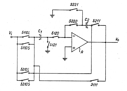
The sample and holds arrangement according to figure 2 com-
prises an vperational amplifier A, capacitors C1 and C2 and
switches S110~ S111, S120, S121, S210, S21~1, S220 and S221. In
order to improve th circuit the switches S110, S121, S210 and S221
are in a preferred embodiment relatively large switches, so that
they have a low res1stance in their conductive state in order to
rapidly charge the capacitors C1 and ~2 to the input voltage Vi.
The other switches may be made smaller than S110, S121, $210 and
S221, because when they are in the conductive state in most cases
the operational amplifier A will b the speed-limiting element.
The accuracy of the sample and hold arrangement`is ~nfluenced
by the clock feedthrough occurring during switching on S111 and
S211 and switching off S110 and 5210. This effect is smaller when
the switches are smaller, for instance, when they have minimrm
W ~ 93/17436 ~13 0 ~ 6 7 PC~INL93/00038
dimensions. In many cases a minimum dimension of S110 and S210 is
not desirable because of the sample rate of the circuit. This may
be solved by a parallel circuit of a large switch (S110L, S210L)
and a switch having minimum dimensions (S110S, S210S~. During
S switching off of this switching combination first of all the large
switch is switched off a shor~ time later follow~d by switchin~ off
the small switch. In this way switching effects of the large ~witch
are short circuited by the small switch after` which the small
switch is opened. The operation of said switches will be
hereinafter explained referring to figures 4a to 4f.
To further reduce the inaccuracy caused by the clock feed-
through the capacitors C1 and C2 may be made relatively large and
may be, for instance, 15 pF.
Switches S11OL/S110S and S21OL/S210S are connected at one
side to the input voltage Vi. The other side of the switches
S11OL/S110S is on the one hand connected to capacitor C1 and on the
other hand to one side of switch S111. Switch S111 is at its other
side connected to the output of the operational amplifier A. The
other side of C1 is connected to the one side of switch S120, as-
well as to the one end of switch S121. The other side of switch
' S121 is connected to a reference voltage, for instance ground. The
3 other side of swit~h S120 is connected to the inverting input ofthe operational amplifier A, the non-inverting input of which
receives the reference voltage (or ground).
2S The other side of the switches S21OL and S210S are connected
to both the~ one~ side of switch S211 and to the one side ;of
~,~ capacitor C2. The other side of switch 5211 is connected to the
output of the~operational amplifier A. The other side of capacitor
C2 is connected to the one side of switch S220 and to the one~side
:i .
~i 30 of switch S221. The other side ~of switch~S220 is oonnected to the
'l ~ invertin~ input of the operational amplifier A, while the other~
slde of switch S221 is connected to the reference voltage (or
ground ) .
Figure~ 3 shows a realization of the circuit according to
figure 2, except for the operational amplifier ~, in CNOS-technol-
I ogy. The polnt OPNEG is connected to the inverting input of the
9 operational amplifier A, the point OPO~T to the output of the oper-
ational amplifier A and the point REF to the reference voltage (or
i
,~j
W O 93/17436 ~ ~ 3 0 ~ 6 ~ 6 PC~NL93/00038
ground). Regarding the other elernents the circuit of figure 3 is,
after figure 2, self explanatory and a further description thereof
may be omitted.
Figures 4a to 4f explain the operation of the circuit accord-
ing to figures 2 and 3. The circuit according to figure 4a serves
as a starting point, in which fiqur~at a certain moment a voltage
Vi(n~ is applied as input signal to the sample and hold arrange-
ment. The output voltage Vo of the operational amp~ifier A is still
equal to the voltage Vi(n-1) of the preceding sampled input signal.
Vi(n~ is stored on capacitor C1. Therefore he switches S110L,
S110S and S121 are closed, while switch S120 is opened. The output
of the operational amplifier ~ is fed back to its inverting input
through capacitor C2 by closing switches S211 and S220. The other
switches are all opened. At the right side of figure 4a the states
of the different switches is described. This also applies to the
figures 4b to 4f.
The switch S121 is opened (figure 4b), so that the capacitor
C1 is not connected to the reference voltage (or ground) any more.
Therefore, the voltage across C1 becomes equal to Vi(n)~Vcfl21,
1 20 where Vcf121 is the voltage change caused by the clock ~eedthrough
du~ing opening the reIatively large switch S121.
Then capacitor C1 is connected to the inverting input of the
opsrational amplifier A through switch S120 (figure 4c). Aft~r a
short setting ~ime the voltage across C1 becomes equal to Vi(n)-
Voff, where Voff is the offset voltage at the input of the oper-
;ational amplifier ~. The resulting voltaqes of the offset voltage
` ~and the clock feedthrough are stored ln~capac1tor C2. Cconsequently
Vo changes ineo: Vo =~Vi(n-1)+Voff+Vcf, where Vcf is~ the total
voltage cha~ge resulting:from both the clock feedthrough of switch
S121 and switch S120. ~he voltage change at the~output ~s in the
order of some mV. It is observed that the voltage across capacito~r
C1 is only determined by Vi(n) and Voff and not by the~clock ~eed-
through of switches S121 and S120. ~ ~
Durin~ the steps of the figures 4a, 4b and 4c capacitor C1 is
connected to Vi through the relatively large switch 511OL and the
smaIl switch S110S. After that capacitor C1 is disconnected from Vi
3 in preferably two steps (figure 4d). First the relatively large
~switch S110L is opened, while the small switch 5110S is still
,,
W 0 9~l7436 2 ~ 3 0 1 6 7 PCTtNL93/00038
closed. Therefore, the error signal caused by the clock feedthrough
necessary to open switch S11OL is short circuited through switch
S11OS. In figure 4d this is indicated by a resistor R.
Consequently, the voltage across capacitor C1 still equals
Vi(n)-Voff.
Then alsc switch S110S is opened, so that capacitor C1 is
entirely disconnected from Vi (figure 4e). At the same tim~
capacitor C2 is disconnected from the operation~ amplifier A by
opening the switches S211 and S220. Opening switches S110S and S220
causes a small error voltage on capacitor C1 caused by the clock
feedthrough, which, however, may be limited for switches S110S and
S220 may have minimum dimensions. Capacitors C1 and C2 are prefer-
ably chosen relatively large, for instance 15 pF, which further
reduces the last-mentioned error voltage. By choosing capacitors C1
and C2 relatively large, moreover, the drift of the output voltage
during the hold phase is reduced. It is observed that the applica-
tion of a small switch S110S parallel to S110L is not essential to
the invention. Switch S110S (and S210S~ may be omitted. In that
case the entire step corresponding to figure 4d is omitted.
Duri~g the situation of figure 4e the output voltage Vo of
the sample and hold arrangement i-s indefinite during a shor~ time.
Therefore, the sltuation~of figure 4e has~to last as short as poss-
ible, preferably less than 10 ns. When thîs phase lasts less than
i
1 10 ns the finite limlted speed of the operational amplifier A will
~ 25 prevent Vo from~ substantially chang1ng during this indefinite
I ; ~ per~iod.
Figure 4f~shows~the i~last~step necessary~ to make the output
voltage~ ~equal to Vi(n). Therefore switch~ S111 is closed, which
connects the output of;the operational~amplifier~ A~to~the slde of
capacitor C1 connected ;to the input Yoltage vi(n). ~lso this~step
introduces an error voltage caused ~y the clock feed~hrough, but
: :
also this error voltage is very small for switch S111~ may also have
mi~imum dimensi~ons. Negleotlng the error voltages on capacitor C1
caused by the~ clock~feedthroug!- from the steps 4eiand~4f the volt-
age across capacitor C1, therefore, all the time equals Vi(n)-~off.
~ecause switch 5~120 remains closed the offset voltage~ Voff at~the
input~of the~operational amplifier A is added to the voltage across
i the capacitor C1 and the output oltage Vo becomes equal to:
i~ :
~::
2,~,3046~
W O 93~17436 ~ P{~/NL93/00038
,' '~
Vo = Vi(n)-Voff+Voff = Vi(n). At the beginning of the steps carried
out in the situation of figure 4f the side of capacitor C2 con-
nected to the inverting input of operational amplifier A is con-
nected to the reference voltage tor ground) by closing switch S2~1.
The circuit remains in the situation of figure 4f as long as
the voltage Vi~n) has to be held and a new voltage Vi(n~1) has to
be sampled. When a new voltage Vi(ni1) has to be sampled switches
S210L and S210S are both clo`sed. Therefore the open side of
capacitor C2 (figure 4f) receives the new voltage Vi(nl1) which is
then stored on capacitor C2. The circuit is then in the same situ-
ation as that of figure 4a, except that the capacitors C1 and C2
have changed position.
The error voltage caus~d by offset compensation of the sample
and hold circuit according to the invention depends on the hold
time and the duration of the situation shown in figures 4c and 4d.
When a hold time of 1 ms, an offset voltage of Voff = 5 mV and a
period of 2 ~s between the situat:ions of figure 4b and figure 4f is
supposed the error voltage in the output signal Vo will approxi
mately be equal to t2 ~s/1 ms) * !; mV = 10 ~V.
Figure 5 shows a simulation result of the operation of the
circuit according to the invention in which at each voltage change
from the output signal Vo it is indicated to which step of ~igure
4a to figure 4f it belongs. The values along both axes only serve
as an example and depend on the dimensions of the switches, the
capacitor values and the speed of the operational amplifier.
The accuracy of the circuit depends on the dimensions chosen.
A~ accuracy w1thin the range of 100 ~V may be realixed. In a pro-
duction process having minimum channel lengths of 1.5 ~m the entire
circuit, including coDtrol logic and hold capacitors of 15 pF, but
excluding the operational amplifier A, may be reallzed on a surface
of 0.2.10-6 m2.
As explained above the output voltage Vo of the sample and
hold arrangement is only indefinite during the phase of figure 4e
during a very~short time period. In practice the output voltage
will then preserve substantially the same value as it had during
the phase of figure 4d (or 4c if no small switches S110S and S210S
are applied. Therefore, aft~r the sample and hold arrangement
according to the invention a low pass filter may be used to recon-
W O 93/17436 213 0 4 6 7 PCT~NL93/00038
struct the original signal. Consequently, the sample and hold
arrangement according to the invention may supply a discrete-time
or a continuous-time signal.
:
: