Note: Descriptions are shown in the official language in which they were submitted.
2 ~ 3 0 6 ~ j AEM 2367 R
POLYMERIC THERMO-OPTIC DEVICE
The invention pertains to a polymeric thermo-optic device comprising a
polymeric optical waveguide and a heating element, the polymeric
waveguide having a layered structure comprising a polymeric guiding
layer ~core layer) sandwiched between two layers having a refractive
index lower than that of the guiding layer (cladding layers).
Thermo-optic devices are known, e.g. from the description given by
Diemeer et al. in Journal of Lightwave Technology, Vol.7, No.3 (1989),
pp 449-453. Their working is generally based on the phenomenon of the
optical waveguide material employed exhibiting a temperature dependent
refractive index (polarization independent thermo-optic effect). Such
devices have been realised, int.al., in inorganic materials such as
~ 15 ion-exchanged glass and titanium-doped lithium niobate. The use of
¦ all-polymeric waveguides for thermo-optic devices has also been
! disclosed, an advantage thereof described by Diemeer et al. being that
~: a modest increase in temperature may result in a large index of
refraction change. The device described by Diemeer is an all-polymeric
planar switch. Switching is achieved by employing total internal
reflection from a thermally induced index barrier. The device
comprises a substrate (PMMA), a guiding layer (polyurethane varnish),
and a buffer layer (PMMA), with the heating element being a silver
stripe heater deposited by evaporation upon the buffer layer through a
mechanical mask. A typical switching speed disclosed is 12 ms for
changing from the deflected state (on state) to the transmitted state
(off state), and 60 ms for changing from transmission to deflection.
A thermo-optic switching device has also been disclosed by Mohlmann et
al. in SPIE Vol. 1560 Nonlinear Optical Properties of Organic
Materials IV (1991) pp 426-433. Use is made of a polymer in which a
waveguide channel can be created through irradiation. The disclosed
device is a polarisation/wavelength insensitive polymeric switch
:.
. ':
:
213~0~
AEM 2367 R
:.
.: .
; comprising an asymmetric Y-junction. The switching properties are
based on heat-induced refractive index modulations causing variations
in the mode evolution in such asymmetric Y-junctions. The device
comprises a glass substrate and a polymeric multilayer comprising an
NL0 polymer. The multilayer structure is not specifically shown. The
disclosed switching time is of the order of milliseconds. The
disclosure refers to devices that are attractive in those locations of
the network where slower switches are permitted. Another thermo-optic
' 10 device disclosed is a thermo-optically biassed electro-optic Mach
Zehnder interferometer.
. ~
Light beam deflection caused by a local refractive index change in
polymer optical waveguide films has been described by Yamada and
~ 15 Kurokawa in Japanese Journal of Applied Physics, Vol. 21 No. 12
`, (1982), pp 1746-1749. Disclosed is applying an RF electric voltage to
a polymer waveguide film to raise the temperature by dielectric loss
heating. The local refractive index change caused by this heating
leads to an incident light beam being deflected in the film plane. A
typical deflection speed disclosed is 150-200 ms.
In Electronic Letters, Vol. 24, No. 8 (1988), pp 457-458 an optical
switch is disclosed in which optical fibres are coupled using a
single-mode fused coupler having a silicone resin cladding material
provided onto the coupling region. Switching is achieved by a
thermally induced refractive index change of the silicone cladding.
Typical switching times disclosed are 5 ms for reaching the on-state
and 80 ms for reaching the off-state.
'.1
In US 4,753,505 a thermo-optic switch is described comprising a
layered waveguide in which the material having a temperature dependent
refractive index is a polymer or glass. The waveguide has a
conventional structure of a core layer sandwiched ~n between two
cladding layers having an index of refraction which is lower than that
of the core layer.
i~
- 21306~
AEM 2367 R
Background art further includes:
EP 306 956, from which it is known to employ the thermo-optic effect
to correct wavelength shifts that occur in directional couplers due to
fluctuations of structural parameters during the process of
manufacturing. To this end, a layered waveguide structure is provided
in which core waveguides and a cladding are successively stacked on a
low refractive index layer, the cladding being provided with a thin
film heater.
L'Onde Électrique, Vol. 71, No. 4, July 1991, p87, from which a hybrid
layered waveguide structure is known. The waveguide is used for
electro-optic modulation, and comprises a polymeric core (doped PMMA)
which on three sides is surrounded by a polymeric cladding (neat
PMMA), and in which the lower cladding layer is silicon on glass.
EP 442 779, from which a conventional, symmetric layered waveguide
structure is known in which the core layer is provided with a
waveguide channel by way of a ribbon having a low refractive index.
EP 281 800 from which a layered waveguide structure is known, the
consecutive layers being a substrate, a low refractive index layer,
and a cladding layer. In the cladding layer a core (channel) is
provided having a higher refractive index than the surrounding
material.
While the disclosed polymeric thermo-optic devices sufficiently
establish that thermo-optic effects can be employed to achieve, e.g.,
switching, the known devices are too slow for practical usage.
Notably, if commercially viable thermo-optic devices are to be
attained, there is a need to further decrease the switching power and
the response time.
To this end the invention consists in that in a polymeric thermo-optic
device of the type identified in the opening paragraph the cladding
layer adjacent to the heating element has a lower refractive index
than the other cladding layer.
2 1 3 a 6 0 5 AEM 2367
.; ,
; A device according to the invention may be built up, e.g., as follows.
Underneath the polymeric waveguide is a support, e.g. a glass or
silicon substrate. On the substrate the following successive layers
can be identified: a lower cladding layer, which may be glass, but
preferably is polymeric, a polymeric core layer (guiding layer)9 and
an upper cladding layer, which also is preferably polymeric but can be
made up of other materials, e.g., glass. The polymeric core layer is
the actual waveguiding layer, the two cladding layers having an index
of refraction which is lower than that of the core layer. On top of
the upper cladding is placed the heating element. The structure in
accordance with the invention is now such that the upper cladding has
a lower refractive index than the lower cladding. By virtue of the
increased RI contrast between the core and the upper cladding, the
upper cladding can be made thinner than usual, and the overall
thickness of the layered waveguide can be even further reduced. This
has several advantages. E.g., the response time of the thermo-optic
device to a temperature rise induced by the heating element is shorter
than with a symmetric thermo-optic device. For, by virtue of the
shorter distance between the heating element and the core layer the
~ 20 latter will experience a higher temperature, and the desired
1 refractive index change will occur at a faster rate. Also, the reduced
heat capacity of the thinner overall structure leads to a faster
cooling and heating rate, hence the invention enables a faster change
of the core's refractive index. A further advantage associated with
the shorter distance between heating element and core is that a better
control is achieved of the position of the heated zone (dissipation of
heat to zones that should not be heated can be substantially
decreased, which means a direct improvement of the function of the
thermo-optic device).
.1
In a particularly preferred embodiment of an all-polymeric waveguide
structure, the lower cladding layer is made up of two sublayers, the
lower of which (i.e., the one adjacent to the substrate) is a thin
. .
:
2~3~0~ AEM 2367 R
layer (e.g. about 3 ~m) having a lower index of refraction than the
other sublayer (i.e., the one adjacent to the core layer). This
additional low index layer has the advantage of preventing the
propagated light from radiating into the substrate. Thus, the actual
waveguiding structure is "optically isolated" from the substrate. This
is particularly important if the substrate is one chosen for its heat-
dissipating properties rather than for its refractive index. Silicon,
e.g., is an excellent heat sink, but has a higher index of refraction
than the layers making up the waveguide. Radiation of propagated light
1 lO into the silicon substrate cannot be prevented. This may lead to loss
; of light, but in particular it makes it difficult to determine exactly
; which portion of the light actually propagates through the layered
waveguide. The additional low index layer provides the certainty that
all the light will propagate through the waveguide. This considerably
facilitates designing the layered waveguide. In order to not affect
the thermal profile, it is preferred that in the presence of the
additional low index layer the total thickness of the layered
waveguide not be affected. By virtue of polymeric materials being
chosen rather than inorganic materials, this can be realized in a
simple manner.
Devices according to the invention can be used with advantage in
~ optical communication networks of various kinds. Generally, the
¦ thermo optic components either will be directly combined with optical
Z 25 components such as light sources (laser diodes) or detectors, or they
will be coupled to input and output optical fibres, usually glass
fibres. Of particular importance is achieving efficient coupling with
the known standard single mode fibres (SSMF). In order to achieve such
efficient coupling, various modifications (e.g., tapering) can be made
to the fibres. The devices according to the invention, however, allow
refraining from such modifications, which makes for a much reduced
complexity of the process, a lower cost and a higher yield, while
keeping the coupling losses low. This can be achieved by tailoring the
2~3~
AEM 2367 R
layered structure of the device, more particularly the layer widths
and the refractive index contrasts, so as to match the field profile
of optical waves propagating through the device to that of the optical
waves propagating through the fibres.
It should be noted that SSMFs have a symmetric structure. As a rule,
coupling to a waveguide having an asymmetric core-cladding structure
will lead to higher coupling losses than coupling to a symmetric
waveguide which is optimized for fiber-chip coupling. However, the
refractive index asymmetry makes it possible to reduce the total
thickness of the device (which, as outlined above, is advantageous for
thermo-optic functioning) without seriously affecting the mode match
required for efficient coupling to optical fibres. Additional coupling
losses, while not completely avoidable, are negligible in the devices
of the present invention.
Although the refractive indices of the cladding and core layers form
an important aspect of the present invention, this is chiefly because
the absolute values of the refractive indices determine the refractive
index contrasts between the various layers of the waveguide. Coupling
losses between the wavesuide and the optical fibres connected
therewith depend on the field profiles of the propagating optical
waves, which are determined by the refractive index contrast and the
layer widths. The Fresnel losses are almost directly related to the
absolute refractive index values. When standard fibres are used, these
losses are negligible when the effective index (Neff) of the guided
modes is below approximately 1.60. Neff, which is a term well-known in
the art, depends on, int.al., the geometry of the waveguide and the
refractive indices of core and cladding, and indicates the refractive
index as experienced by a propagating wavefront.
The refractive index of the optical polymers used will generally be
within the range of from 1.4 to 1.8, preferably of from 1.45 to 1.6~.
:~ 213~o~
AEM 2367 R
,.,
The refractive index contrast between the two cladding layers may
vary. The lower limit is mainly determined by whether the effect of
the invention can be attained, i.e., by whether a substantial decrease
is achieved in switching power needed, or in response time, or both.
; 5 The upper limit is mainly determined by the point at which any further
j decrease by and large has no additional effect and/or coupling losses
`', become too high. Said refractive index contrast will mostly be of the
order of 0.005 to 0.05.
If having a low optical loss is more crucial than having a reduced
switching power, it is preferred to provide a waveguide structure that
3 is less asymmetric, i.e., in which the refractive index contrast
~ between the two cladding layers is of the order of 0.005 to 0.01. In
,i particular, this may be the case for a 1*2 switch, in which the power
for only one switching unit is needed, and coupling losses at the
input and output fibres make a large contribution in percentage terms
to the efficacy of the switch. In the case of an n*m switch, n and m
being integers ~2, which comprises a cascade of 1*2 and/or 2*2
switches having a single input and output optical fibre, the coupling
il 20 losses make a less signifcant contribution, and a reduced switching
power is of more importance in view of the higher number of switching
units to be operated. In such a case it is preferred to have a high
refractive index contrast, i.e. of the order of 0.03 to 9.05, so as to
allow the thinnest possible cladding layer adjacent to the heater. In
most cases, however, it will be desired to have the optimal
combination of low optical loss and reduced switching power. To this
end, it is most preferred if the above refractive index contrast is
I within the range of from 0.01 to 0.03.
,~
~ 30 Optical polymers are known, and the person of ordinary skill in the
¦ art is able to choose polymers having the appropriate refractive
indices, or to adapt the refractive indices of polymers by chemical
I modification, e.g., by introducing monomerlc units that affect the
2~ 3~6~ AEM 2367 R
' :
refractive index. As all polymers exhibit a thermo-optic effect,
basically any polymer having sufficient transparency for the
wavelength used can be employed in the core of the waveguide `
component. Said transparency requirement also holds for the cladding.
i 5 Particularly suitable optical polymers include polyacrylates,
polycarbonates, polyimides, polyureas.
The design of the layered polymeric waveguide comprised in the devices
according to the present invention generally depends on the exact
function that the thermo-optic device has in the optical network.
Whatever design is required, in the layered (slab) waveguide
structure, in which a core layer is sandwiched between two layers
having a lower index of refraction, it will usually be required to
introduce a pattern of laterally defined waveguide channels, i.e.,
! 15 portions of the core layer that vertically and laterally are adjacent
to material having a lower index of refraction. A waveguide can be
provided with a pattern of waveguide channels in various manners.
Methods to achieve this are known in the art. For example, it is
possible to introduce such a pattern by removing portions of the slab
waveguide, e.g., by means of wet-chemical or dry etching techniques,
~ and to fill the gaps formed with a material having a lower index of
¦ refraction. Or, e.g., photosensitive material that can be developed
after irradiation may be used. In the case of a negative photoresist
the photosensitive material is resistent to the developer after
irradiation, and the portions of the material that were not subjected
to irradiation can be removed. It is preferred to use a positive
photoresist, and to define the channels by means of an irradiation
mask covering the waveguide portions that will form the channels. The
irradiated material then is removed using developer, after which a
material of lower refractive index is applied.
It is more strongly preferred, however, to use a core material that
allows defining a waveguide pattern without material having to be
,;, ... ~ . . .. .. .. .
21~0~ AEM 2367 R
9 .
;removed. Materials of this nature exist, e.g., those that will undergochemical or physical conversion into a material having a different
refractive index when subjected to heat, light, or UV radiation. In
the cases where this conversion results in an increase in the
refractive index, the treated material will be employed as core
material for the waveguide channels. This can be carried through by
employing a mask in which the openings are identical with the desired ~-
waveguide pattern. In the case of the treatment leading to a decrease
of the refractive index, the treated material is suitable as a
cladding material. In that case a mask as mentioned above is used,
i.e. one that covers the desired waveguide channels. A particular, and
preferred, embodiment of this type of core material is formed by
polymers that can be bleached, i.e., of which the refractive index is
lowered by irradiation with visible light or UV, without the physical
and mechanical properties being substantially affected. To this end it
is preferred to provide the slab waveguide with a mask that covers the
desired pattern of waveguide channels, and to lower the refractive
index of the surrounding material by means of (usually blue) light or
UV radiation. Bleachable polymers have been described in EP 358 476.
It is further preferred to employ NLO polymers in the core, in order
to have the possibility of making combined thermo-optic/electro-optic
devices.
Optically non-linear materials, also called non-linear optical (NLO)
materials, are known. In such materials non-linear polarisation occurs
under the influence of an external field of force (such as an electric
field). Non-linear electric polarisation may give rise to several
optically non-linear phenomena, such as frequency doubling, Pockels
effect, and Kerr effect. Alternatively, NLO effects can be generated
opto-optically or acousto-optically. In order to render polymeric NLO
materials NLO-active (obtain the desired NLO effect macroscopically),
the groups present in such a material, usually hyperpolarisable
. 213060~ AEM 2367 R
,'.
,.
sidegroups, first have to be aligned (poled). Such alignment is
commonly effected by exposing the polymeric material to electric (dc)
voltage, the so-called poling field, with such heating as will render
the polymeric chains sufficiently mobile for orientation. NLO polymers
' 5 are described in, int. al., EP 350 112, EP 350 113, EP 358 476,
EP 445 864, EP 378 185, and EP 359 64B.
Making the polymeric optical waveguide of the invention will generally
involve applying a solution of the polymer used as the lower cladding
. 10 to a substrate, e.g. by means of spincoating, followed by evaporating
the solvent. Subsequently, the core layer, and the upper cladding
Z layer, can be applied in the same manner. On top of the upper cladding
the heating element will be placed, e.g., by means of sputtering,
chemical vapour deposition, or evaporation and standard lithographic
. 15 techniques. For fixation and finishing a coating layer may be applied
on top of the entire structure, so as to allow better handling of the
3 device. Alternatively, instead of a coating layer a glue layer may be
3 used for fixation, after which the total structure can be finished by
placing an object glass on it.
When making all-polymeric layered waveguide structures, it is
advantageous to apply the individual layers in the form of prepolymers
~3 that comprise functional end-groups (e.g. OH) and to include a
j cross-linker (e.g. a diisocyanate such as Desmodur-N) so that a cured
~ polymeric network is formed that does not dissolve when the next
¦ 25 layer is provided.
Suitable substrates are, int. al., silicon wafers or plastics
` laminates, such as those based on epoxy resin which may be reinforced
or not. Suitable substrates are known to the skilled man. Preferred
are substrates that, by virtue of a high thermal conductivity, can
function as a heat-sink. This can considerably speed up the
thermo-optic switching process. For, considering that switching to,
say, the "on" state can be reached by heating the waveguide, reaching
I
213`~GO.~ AEM 2367 R
1 1
the "off" state then will require leaving the waveguide to cool. The
preferred substrates in this respect are glass, metal, or ceramics,
and particularly silicon.
It is also possible to employ thermosetting material for making the
polymeric optical waveguide, or a portion thereof (e.g. one of the
layers). If at least the lower cladding is made from a freestanding
thermoset material, it is possible to refrain from using a separate
substrate if so desired, as the lower cladding will perform this
function.
i The heating element will generally be made up of a thin film electric
conductor, usually a thin metal film. Such a thermal energy generating
live electric conductor can also be called "resistor wire" for short.
Of course, suitable thermal energy generating conductors are not
restricted to the wire form.
The thermal energy generating live electric conductor, the resistor
wire, may be a heating element known in itself from the field of thin-
film technology, such as Ni/Fe or Ni/Cr. Alternatively, it is possibleto employ as electric conductor those materials which are known from
the field of electro-optic switches as the ones from which electrodes ~ ~h~
are made. These include noble metals, such as gold, platinum, silver,
palladium, or aluminium, as well as those materials known as
transparent electrodes, e.g., indium tin oxide. Aluminium and gold are
preferred.
If poled NL0 polymers are employed in the present waveguides, using
heating elements that can function as an electrode makes it possible
to combine thermo-optic and electro-optic functions in a single
device.
, ~
~ 213 ~ 6 0 ~ AEM 2367 R
~ 12
.
;
In the case of the functions of the electrode and the resistor wire
' being combined, a surge can be realised in actual practice by, say,
', employing a feed electrode of relatively large diameter (low current
density) followed by a segment having a comparatively small diameter.
A high current density will then be created in this narrow segment, so
that heat is generated. Alternatively, it is possible to employ a
material made up of two metals of different intrinsic resistance, and
~' to vary either the thickness of the different metallisations or the
, composition of the material in such a way as to obtain the desired
effect of a low current density, or a low intrinsic resistance upon
supply, while a high current density or a comparatively high
intrinsic resistance is displayed at the location where the
thermo-optic effect is desired. By thus varying current densities it
-~ is possible to locally obtain a thermo-optic effect.
In the case of NLO polymers being employed, the heating element may be
put to initial use during the alignment of the NLO poly~ers.
~ The invention is further illustrated with reference to the following
¦ unlimitative Examples and the accompanying drawings.
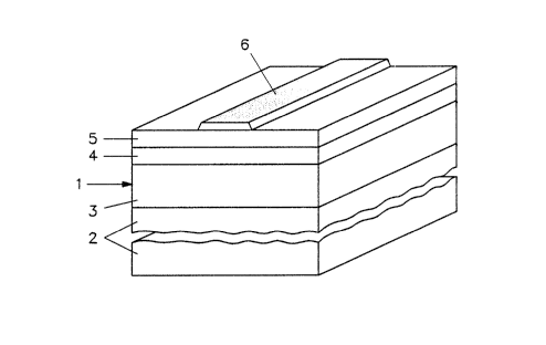
Figure 1 shows a layered polymeric waveguide (1) having an asymmetric
structure. The layered waveguide comprises a substrate (2), a lower
cladding layer (3), a guiding layer (4), and an upper cladding layer
(5). On top of the upper cladding layer (5), is a heating element (6).
The two cladding layers (3,5) have a lower refractive index than the
guiding layer (4). Further, the upper cladding layer (5) has a lower
refractive index than the lower cladding layer (3~, and consequently
can be thinner, as is shown.
`! 30 EXAMPLE 1
The relevant data of several waveguides are given. The waveguides are
comprised of a layered structure in which, on a substrate (S), the
213060~ AEM 2367 R
13
following successive layers can be identified: lower cladding layer
(L), core layer (C), upper cladbing layer (U), and heating element
(H), i.e., as follows (see also Figure 1):
.'
HHHHHHHH
UUUUUUUUUUUUUUUUUUUUUUU
CCCCCCCCCCCCCCCCCCCCCCC
LLLLLLLLLLLLLLLLLLLLLLL
., SSSSSSSSSSSSSSSSSSSSSSS
The exemplified core layer (C) thicknesses vary from 2-9 ~m. The lower
cladding (L) in each case is a layer of an optical polymer having a
refractive index of 1.58. For the upper cladding are selected
materials with three different refractive indices, viz. 1.56, 1.57,
and 1.58, i.e., with ~RI between the two claddings being 0.02, 0.01,
and 0 respectively. The third one is a symmetrical waveguide (not in
` accordance with the invention). The core layer in each case has a
refractive index higher than that of the two claddings, the optimal RI
varying between 1.583 and 1.589.
Table 1 shows the cladding thicknesses that can be employed when the
waveguide of given core layer thicknesses and refractive indices is to
be coupled to an SSMF while retaining the required mode match (if the
cladding thicknesses are lower, light will be absorbed by layers
outside the cladding, such as the heating element or the substrate,
, which leads to a considerable propagation loss). The man skilled in
! the art can determine which layer thicknesses are possible by
calculating the overlap between the modal field of the SSMF and that
of the waveguide. Thicker claddings could be employed, but this would
I 30 needlessly reduce the benefit to be had from the invention due to
i increased heat capacity. The upper limit for the core thickness is
mainly determined by the point at which the waveguide becomes
multimode for the oiven wavefront. This is undesirable, as it leads to
2130~
AEM 2367 R
14
a less precise functioning of the device, and the higher order modes
generated cannot be coupled into an output SSMF. The man skilled in
the art can determine the point at which a waveguide becomes
undesirably multimode by means of the known waveguide dispersion
relation.
TABLE 1
Upper cladding thickness
(~m)
Asymmetric Symmetric
~RI 0.02 ~RI 0.01 ~RI 0
Core Thickness
(~m)
2 3.17 4.56 17.57
3 2.99 4.3~ 15.67
4 2.85 4.13 14.42
2.73 4.00 12.70
6 2.63 3.84 11.05
7 2.53 3.68 9.31
8 2.42 3.50 7.60
9 2.30 3.24 5.96
From Table 1 it is clear that, in each case, the asymmetric waveguide
according to the invention has a lower upper cladding thickness than
the symmetric waveguide not according to the invention. The waveguides
of the invention thus possess the above-identified advantages
associated with a thinner cladding when used in thermo-optic devtces.
From Table 1 the overall waveguide thicknesses can be computed (in
each case the lower cladding has the same thickness as the upper
cladding in the corresponding symmetric waveguide). The results are
given in Table 2.
213~60~
, . . .
AEM 2367 R
,
:
. TABLE 2
Total waveguide thickness
ym
Asymmetric Symmetric
~RI 0.02 ~RI 0.01 ~RI 0
. Core thickness ~ -
(ym)
2 22.74 24.13 37.14
~ 3 21.66 23.02 34.34
'' 10
4 21.27 22.55 32.84
~` 5 20.43 21.70 30.40
', 6 19.68 20.89 28.10
7 18.84 19.99 25.26
`i 8 18.02 19.10 23.20
j./ .
~ 9 17.26 18.20 20.92
,'~ ,
From Table 2 i t is clear that in each case the asymmetric waveguide ~-
according to the invention is thinner than the symmetric waveguide not
' in accordance with the invention. In the case of a core thickness of
9 ym, the overall thickness of a symmetric waveguide is relatively
low, but in the case of this waveguide being optimized for fiber to .
chip coupling a 9 ym core causes the waveguide being multimode, which
is undesirable. ;~
1: In Table 3 the coupling losses incurred with the various exemplified
!~, waveguides are given. The wavelength employed was 1.3 ym.
`1~
~ 30
~,
A
.,
~ .
213360~ AEM 2367 R
16
., ~
TABLE 3
Calculated coupling loss
(dB)
Asymmetric Symmetric
~RI 0.02 ~RI 0.01 QRI 0
; Core thickness
(~m)
2 0.691 0.526 0.144
3 0.461 0.355 0.107
' 4 0.301 0.231 0.075
S 0.191 0.144 0.048
6 0.116 0.086 0.028
7 0.068 0.044 0.015
8 0.039 0.028 0.009
9 0.026 0.020 0.012
From Table 3 it is clear that, in each case, the asymmetric waveguide
according to the invention displays a somewhat higher coupling loss
than the symmetric waveguide not in accordance with the invention.
However, a difference in loss of lower than about 0.1 dB is considered
negligible, and it is clear that with the invention a favourable
combination of low upper cladding thickness, low overall waveguide
thickness, and low coupling loss is achievable. In the case of the
listed exemplified waveguides, those with core thicknesses of 7 and 8
~m are preferred in this respect.
EXAMPLE 2
For two thermo-optic Y-shaped switches, i.e., switches having one
input channel and two output channels (made in the guiding layer of a
213~60a
17 AEM 2367 R ~ ~
., .
- layered waveguide with an asymmetric structure such as depicted in
Figure 1), response times were determined.
In cross-section, the waveguide can be indicated schematically as in
Example 1 and Figure 1. The basic Y-shaped waveguide channel design
, used is indicated schematically in Figure 2.
Figure 2 shows a top view of the waveguide channels. Light enters the
waveguide via channel ~7). Due to the asymmetry of the Y's legs (8)
and (9) - not to be confused with the asymmetry of the waveguide's
layers! - the light propagating through the waveguide will be directed
through leg (8). This is defined here as the "off" state.
On the basis of the Y-shaped channel waveguide shown in Figure 2, a
thermo-optic switch was designed in accordance with Figure 3.
Figure 3 shows a top view of the waveguide channels. Light enters the
waveguide via channel (7). A heating element (10) is placed at leg
¦ (8). This enables leg (9) to be activated: when the heating element is
turned on, by applying a 15 mW surge, the refractive index decreases
locally at the part of leg (8) underneath heating element (10) to such
an extent that the propagating light will be directed to leg (9). This
~ is defined here as the "on" state.
1 25 The response time for reaching the state defined as "on" was less than
1 ms. The response time for reaching the "off" state, by turning the
heating element off and thus allowing the refractive index to retain
the original value, was about 4 ms.
/ .
. .
2~3~605
AEM 2367 R
18
. .
-. EXAMPLE 3
A second thermo-optic switch was designed, see Figure 4.
. 5 Figure 4 shows a top view of the waveguide. Light enters the waveguidevia channel (11). The symmetric legs (12) and (13) are provided with
heating elements (14) and (15). When one heating element is turned on,
say heating element (14), the refractive index of the part of the
waveguide's leg (12) underneath it decreases locally to such an extent
~ 10 that the propagating light will be directed to the other leg, in this:~ case leg (13). This being defined as the "on" state, the "off" state
~P now can be reached by employing heating element (15)~ and turning off,, heating element (14), so as to have the refractive index of leg (13)
~i decrease and that of leg (12) increase back to the original value,
:~ 15 thus having the light directed to leg (12).
.,
The response time for reaching either state was about 1 ~s.
s~
,
~ 20
'''I ~
i:~ 25
1 30
.: