Note: Descriptions are shown in the official language in which they were submitted.
WO 93/18428 ~ 3 ~ ~ 7 2 PCI/US93/0231
HEAD--MOUNTED DISPLAY SYSTEM
Background of tbe Invention
Head mounted display systems have been developed
for a number of different applications including use by
aircraft pilots and for simulation. Head mounted
displays are generally limited by their resolution and
by their size and weight. Existing displays have
relatively low resolution and are positioned at a
relatively large distance from the eye. Of particular
importance, is to keep the center of gravity of the
display from extending upward and forward from the
center of gravity of the head and neck of the wearer,
where it will place a large torque on the wearer's neck
and may bump into other instru~ents during use. There
is a continuing need to present images to the wearer of
a helmet mounted display in a high-resolution format
~imilar to that of a computer monitor. The display
needs to be as non-intrusive as possible, leading to
the need for a lightweight and compact system.
Head mounted displays can also utilize eye
tracking systems in flight control, flight simulation
and virtual imaging displays. Eye control systems
generate information based on the position of the eye
with respect to an image on a display. This
information is useful for a variety of applications.
It can be used to enable the viewer to control "hands-
free" movement of a cursor, such as a cross-hair on the
display.
Apparatus for detecting the orientation of the eye
or dete~mining its line-of-sight ~LOS) are called
occulometers or eye trackers and are well known in the
. art. (See for example U.S. 4,109,145, 4,034,401 and
4,Q28,725).
WO93/1~28 PCT/US93/02312
6 ~ 2
Summarv of the Invention
In accordance with the present invention a head
mounted di~play is preferably either an
electroluminesaent (EL) or an active matrix liquid
crystal di~play (AMLCD) comprising thin film transistor
(TFT) driving elements formed of single crystal silicon
and then transferred to a transparent glass substrate.
Each TFT circuit is connected to an electrode which
defines a picture element (pixel) of the display. The
head ~ounted di~play system can also include a detector
array comprising thin film integrated optical diode
detectors is formed of III-V materials and transferred
directly onto a flat panel active matrix display.
In a preferred embodiment of a direct view eye
tracking dispaly, the detectors are positioned such
that each i~ completely above the drive transistors of
the active matrix circuit i.e., adjacent to the pixel
area and therefore do not block any of the display's
- light output. The light output $rom the display,
either infrared or visible, is used to determine the
po~ition of the eye. No additional optics, such as,
fiber optics to/from remote displays are required in
this approach. The chief advantage is that the
integrated eyetracker/display can be inserted in a
helmet-mounted optical system without physical
modification to the helmet or optics This advantage
results from the fundamental reciprocity of the axial
light r~ys that are used to determine the eye position.
! 'An ax~a~ ray, is a light ray that emanates from the
dispiay and travels through the optical axis of the
eye, nsrmal to the retina. These rays, when reflected
by the retina, can travel back to the display along the
same optical path (in accordance with the optica}
~ , -
;
W093/18428 2 l 3 ~ 6 7 2 PCT/US93/02312
reciprocity theorem). Except for divergence of the
rays, thie reflected ray~ return to the vicinity of the
emitting pixel. In this way, the detector can identify
the area of the display that i8 sighted by the user.
Software in a computer then provides a cursor at this
location.
In ~nother alternative emkodiment, instead of
using the visible scene from the displaiy, somei of thie
frames in the display are used for brief presentation
of an interlaced eyetracker pattern. If the repetition
rate of the test pattern is sufficiently infreguent,
the user (viewer) will not perceive its presence. This
pattern can consist of a single pixel being illuminated
or can haive some other geometric pattern. Light from a
single lit pixel enters the eye through the pupil and
is refle¢ted from the retina. The path of the
reflected light clearly depends on the position of the
eye. On the reverse path back to the display panel,
the reflected light undergoes spreading or convergence
depending upon the optical system. As it returns to
the plane of the display, it strikes the
photodetectors. A pattern will appear in the output of
the photodetector array that depends on the position of
the eye and the nature of the optical system. This
pattern is interpreted by a computer and correlated to
the position of the eye.
- m e present invention uses a single-crystal
material to produce a high-density active matrix array
in a h~d mounted optical support system that provides
for closeness of the display to the eye, compactness of
the array and provides the desired level of resolution.
With a density of 400 lines per centimeter, for
example, a 1.27 centimeters display in accordance with
WO93/18428 PCT/US93/02312
213 '~57 ~
-4-
the invention will fit into a system only 1.52
centimeters in depth. This system is more compact, has
lighter weight, and a lower cost than existing head
mounted displays.
To get the display system as clo~e as possible to
the eye and as co~pact as possible, 2 short focal
length lens system must be used. The focal lengths of
simple lenses are limited by lens geometry, where the
thickness of the lens is less than the lens diameter.
Thus, a simple lens has a shorter focal length as well
as a small diameter. For the most compact system, the
smallest poss~ible lens that focuses the display image
is used. The lens size is defined by the object size,
which in this case is the size of the display element.
lS Since resolution needs to be increased while size
needs to be decreased, the pixel density of the display
needs to increase. Existing displays have pixel
densities of about 120 lines per centimeter and are
about 4.1 centimeters in diameter. Using a 3.81
centimeter lens, where the minimum focal length for a
standard 3.81 centimeter lens is about 3.05
;~ centimeters, results in a lens with a center thickness
of over 1.52 centimeters. The use of this lens results
in a lens-to-display distance of about 3.3 centimeters,
which is the minimum depth of an existing head-mounted
display for this geometry.
The present system, by increasing the pixel
denæity to at least 200 lines per centimeter, and
` preferq~ly to over 400 lines per centimeter, provides
for a lens-to-display distance of less than one inch.
The len~-to-display distance is preferably in the range
of~ 1.0-2.2 centimeters.
" ,i; ~
. . -., . i - ~ , , .
." " ~ " ~
.,,, ~ , ,
W093/18428 2 1 3 ~ ~ 7 2 PCT/US93/023t2
The displsy can be a transmission type display
with the light source directly adjacent the light valve
active matrix or the liqht source can be positioned
above the head or to one or both side~ of the head of
the user such that the light can be coupled to the
light valve active matrix by one or more reflective
elements. Fiber optics can also be employed to provide
a back light source for the display or to deliver
i~ages from the display into the user's field of view.
Alternatively, the display can be an emission type
device such ~s an active matrix electroluminescent
display or an active matrix of light emitting diodes
(LEDs).
Additional embodiments of the invention include a
projected view active matrix display in~which different
polarization components of light are ~eparated, one
co ponent being directed to the left eye, and another
co~mponent being directed to the right eye. Thi~
provides a more efficient optical system in which more
light from the 50urce is used to provide the desired
image.
Another preferred embodiment utilizes an active
matrix display in which the pixel size increases across
the display to provide a wide angle field of view
display.
The display can be fabricated as a visor with a
nu~ber of displays which are tiled together and
positioned on a flat or curved plastic visor.
~rief Descri~tion of ~he Drawinas
Figure 1 is a perspective view of a high density
circuit module in the form of an active matrix liguid
crystal display (AMLCD).
6 ~
WO93/18428 PCT/US93/02312
30672
--6--
Figure 2A is a schematic illustrating how two six
inch wafer~ can be used to form tiles for a 4 X 8 inch
AMLCD.
Figure 2B shows the tiles of Figure 2A applied to
a glass substrate for forming an AMLCD.
Figure 3 is a circuit diagra~ illustrating the
driver system for the AMLCD of Figure 1.
Figures 4A-4L is a preferred process flow sequence
illustrating the fabrication of the a portion of the
circuit panel for the AMICD of Figure 1.
Figures 5A and SB are cross-sectional schematic
process views of a portion of the AMLCD.
Figure 6 illustrates in a perspective view a
preferred e~bodiment of a system used for
recrystallization.
Figures 7A-7D is a process f low sequence
illustrating transfer and bonding of a silicon an oxide
(SOI) ~tructure to a glass superstrate and removal of
the substrate.
- 20 Figures 8A and 8B is a process ~low sequence
illustrating an alternative transfer process i-n which a
GeSi alloy is used as an intermediate etch step layer.
Figure 9 is a schematic diagram of an eye tracking
system of the invention.
Figure 10 is a schematic of an alternate
e~bodiment of an eye tracking system of the invention.
Figure 11 is an exploded view of the integrated
display/detector array panel (eye-tracker) of the
inven~fon.
Figure 12 is a plan view of a simplified version
of the eye tracker in which the matrix array
metallization is replaced by a common parallel
interconnect.
, ,
~,
::
WO93/18428 ~ PCT/US93/02312
Figures 13A-13C are cross-sectioned views showing
important steps in the proces~ of forming the eye-
tracker device of the invention.
Figures ~4A-B are schematic section views of a
S wafer being processing to form an X-Y addressable LED
array.
Figures 14C-E are schematic partial perspectives
showin~ a wafer during successive additional process
steps.
Figures 15A-lSB is a process flow diagram of the
main steps in fabricating an LED bar in accordance with
a mesa etch isolation process with a corresponding
schematic sectional view of a wafer structure so
processed shown beneath each step.
Figure 16 is a cross-sectional side view of a
wafer during step k of Figure 15b.
Figure 17 is a process flow diagram of the main
steps in fabricating an LE~ bar in accordance with an
alternate process with a correspnding schematic
sectional view of a wafer structure so processed shown
beneath each step.
Figures 18A-18B is a process flow diagram of the
main steps in fabricating an LED bar in accordance with
yet another alternate process with a corresponding
schematic sectional view of a wafer structure so
processed shown beneath each step.
Figure 19 is a plan view of an X-Y addressable LED
array mounted on a silicon substrate with asQociated
silicon electronic circuitry.
Figure 20 is a perspective view of a LED pixel
from an X-Y addressable LED array embodiment of the
invention.
' :' '
::,
W093/1~28 PCT/US93/02312
21 ~067 2
Figure 21 is a schematic side view of an IR to
visible light converter embodiment of the invention.
Figure 22 is a schematic diagram of the converter
of Figure 2l.
S Figure 23 is a side view of an alternate
embodiment of Figure 21.~
Figure 24 is a side view of a pixel of a tri-color
X-Y addressable LED array.
Figure 25 is a plan view of the array of Figure
24.
Figure 26 is a schematic diagram of an alternate
embodiment of an eye tracking device of the invention.
Figure 27A is an exploded perspective view of an
electroluminescent panel display in accardance with the
present invention.
Figure 27B is a perspective view of an
electroluminescent color display element.
Figure 27C is a circuit diagram illustrating the
driver system for the electroluminescent panel display.
Figure 27D is an equivalent circuit for a DMOS
transistor of Figure 16C.
Figures 28A-28L is a preferred process flow
sequency illustrating the fabrication of a circuit
panel for an electroluminescent panel display.
Figures 29A-29D is preferred process flow sequence
illustrating the fabrication of an electroluminescent
color display.
Figures 3OA-3OB is a preferred process flow
sequen~é illustrating transfer and bonding of an SOI
structure to a superstrate and removal of the
substrate.
Figures 3lA-3lB is a preferred process flow
; sequence illustrating an alternative transfer process
. ~
WO93/18428 PCT/USg3/0231~
2 1 ~ 7 2
in which a GeSi alloy i8 used as an intermediate etch
stop layer.
Figure 32 shows a schematic illustration of a head
mounted display system.
FigurQ 33 illustrates a preferred embodiment of a
head mounted display where two components of polarized
light are ~eparated for improved optical efficiency.
Figure 34 illustrates an active matrix for a wide
angle field of view head mounted display system.
Figure 35 provides a detailed view of a portion of
the active matrix area of the device shown in Figure
34.
Figure 36 illustrates an active matrix mounted or
ti}ed onto a visor screen.
Figure 37A-37C illustrates other preferred
embodiments of a direct-view display system.
etailed De8cri~tion of the Invention
I. Tiled Active Matrix Liauid Crvstal Displav
A preferred embodiment of the invention for
fa~ricating complex hybrid multi-function circuitry on
- common module substrates is illustrated in the context
of an AMLCD for a head mounted display, as shown in
Figure 1. The basic components of the AMLCD comprise a
light source 10, such as a flat fluorescent or
incandescent white lamp, or an electroluminescent lamp
having white, or red, blue and green p~Qsphors~ a first
polarizing filter 12, a circuit panel 14, an optional
filt ~ late 16 and a second polari2ing filter 17,
which form a layered ætructure. Note that filter plate
16 is not needed for a black and white display or where
the red, green and blue colors are prov~ded by the lamp
at the appropriate pixel. A liquid crystal material
,, ", ,, ~ , ~
"~
WOg3/1~28 PCT/US93/02312
~13~6~2
--10--
23, such as a twisted nematic is placed between tbe
circuit panel 14 and the filter plate 16.
Circuit panel 14 consists of a transparent common
module body 13 formed, for example, of glass upon which
is transferred a plurality of co o on multifunction
circuits comprising control logic circuits 40A and 40B
and drive circuits 18A and 18B, 20A and 20B, and array
circuit 25A and 25B. Preferably, the logic and drive
circuits which require high speed operation are formed
in tiles of x-Si. The array circuits may be formed in
~-Si Daterial, or poly-Si, or preferably in x-Si, to
achieve lower leakage in the resultant TFT's and,
hence, better grey scale. Higher speed is also
achieved in x-Si. Displays as large as a 4 x 8 inch
active ~atrix LCD array can be formed from two standard
6-inch diameter Si wafers Wl and W2 as shown in Figure
2A. Array circuit 25A is formed on wafer Wl and l-inch
by 4-inch tiles TA are transferred from the wafer Wl to
the substrate 14. Note that the transfer can be
accomplished using either a single or double transfer
proc-ss, a8 will be described in detail below.- Each
tile is registered against another using
micropositioning equipment and manipulators capable of
micron scale accuracy. Similarly, tiles TB are
transferred from wafer W2 to form array 25B on
substrate or common module body 13 (See Figure 2B).
Logic circuits 40A and 40B and drive circuits 18A,
18B, 20A, 20B are formed on other suitable substrates
(not ~6wn) and tiled and transferred in like manner to
common ~ubstrate 13 and registered opposite the arrays
2SA, 25B, as shoWn in Figure 1. Conductive
interconnections 50 are then made between the drive
circuits and the individual pixels 22 and the logic
W093/l8428 2 1 3 ~ ~ 7 2 PCT/US93/02312
control circuits 40A and 40B. In this manner, a 1280
by 1024 addre~sablQ array of pixels 22 are formed on
the substrate 13 of circuit panel 14. Each pixel 22 is
actuated by voltage from a respective drive circuit 18A
or B on the X-axis and 20A or B on the Y-axis. The X
and Y drive circuits are~controlled by signals from
control logic circuits 40A and B. Each pixel 19
produces an ~lectric field in the liquid crystal
material 23 disposed between the pixel and a
counterelectrode (not shown) formed on the back side of
the color filter plate 16.
The electrio field formed by pixels 22 causes a
rotation of the polarization of light being transmitted
across the liquid crystal material that results in an
ad~acent color~filter element being illuminated. The
color filters of filter plate system 16 are arranged
into groups of four filter elements, such as blue 24,
green 31, red 27, and white 29. The pixels associated
with filter elements can be selectively actuated to
provide any desired color for that pixel group.
A typical drive and logic circuit that canrbe used
to control the array pixels 22 is illustrated in Figure
:
3. Drive circuit 18A receives an incoming signal from
control logic 40A and sends a signal to each source
electrode of a TFT 51 in one of the columns selected by
logic circuit 40A through interconnect line 53. Y-
drive circuit 20A controlled by logic circuit 40A
energizes a row buss 59 extending perpendicular to
col ~ ss 53 and applies a voltage pulse to each gate
G of TFT's 51 in a selected row. When a TFT has a
voltage pulse on both its gate and source electrode
current flows through an individual transistor 51,
which charges capacitor 56 in a respective pixel 22.
~,
~,
"
WO93/18428 PCT/US93/02312
2 1 ;;~ i) 6 7 2
-12-
The eapaeitor 56 sustains a charge on the pixel
eleetrode ad~aeent to the liquid erystal material
(shown sehematieally at 19) until the next sean of the
pixel array 25. Note that the various embodiments of
the invention may, or may not, utilize eapaeitors 56
with eaeh pixel depending upon the type of display
desired.
II. Transfer Proeesses
-The array eireuits 25A and 25B and logie 40A,40B
and drive eireuits 18A,18B may be formed and
transferred by a number of proeesses. The basie steps
in a single transfer proeess are: forming of a
- plurality of thin film Si eireuits on Si substrates,
` dieing the thin film to form tiles, and transferring
the tiles to a eommon module substrate by "tiling."
Tiling ean also bæ employed in fabrieating III-V
;~ material eireuits or hybrid Si and III-V material
, .
eireuits or eireuit eomponents, whieh ean be ~staeked to
provide eompaet modules.
Tiling involves the steps of transferring f
registering the transferred tiles, and adhering the
registered tiles. The Si substrates are then removed
and the eireuits on the tiles are interconnected. The
double transfer approach, described in detail below in
connection with Figures 4A-4L is similar except that
the Si-substrate is removed after dicing and the thin
film i8 transferred to an intermediate transfer body or
earrie~'before ultimate transfer to the common module
body.
Assuming an Isolated Silicon Epitaxy (ISE) process
is used, the first step is to form a thin-film
preeursor strueture of silicon-on-insulator (SOI) film.
W093/18428 ~ 3 'i 7 ~ PCT/US93/02312
-13-
An SOI structure, such as that shown in Figure 4A,
includes a substrate 32 of Si, a buffer layer 30, of
semi~insulating Si and an oxide 34 (such as, for
exa~ple, SiO2) that is grown or deposited on buffer
S layer 30, usually by Chemical Vapor Deposition (CVD).
An optional release layer 36 of material which etches
slower than the underlying oxide layer 34 is then
formed over the oxide 34.
For example, a silicon oxy-nitride release layer,
comprising a mixture of silicon nitride (S3N~) and
silicon dioxide (SiO2) may be a suitable choice. Such
a layer etches more slowly in hydrofluoric acid than
does sio~ alone. This etch rate can be controlled by
adjusting the ratio of N and O în the silicon oxy-
nitride (SiO~) compound.
A thin essentially single crystal layer 38 of
-~ silicon is then formed over the release layer 36. The
oxide (or insulator) 34 is thus buried beneath the Si
surface layer. For the case of ISE SOI structures, the
~ 20 top layer is essentially single-crystal recrystallized
- ; silicon, from which CNOS circuits~can be fabri~ated.
Note that for the purposes of the present
~;~ application, the term "essentially" single crystal
mæans a film in which a majority of crystals show a
common crystalline orientation and extend over a cross-
- sectional area ih a plane of the film for at least 0.1
cm2, and preferably, in the range of O.S - 1.0 cm2, or
more. The term also includes completely single crystal
Si. m ë thin films can have thicknesses in the range
of 0.1 - 20 microns and preferably in the range 0~1 -
1~0 microns.
W093/1~28 PCT/US93tO2312
~13~72
-14-
The use of a buried insulator provides devices
having higher speeds than can be obtained in
conventional bulk (Czochralski) material. Circuits
containing in excess of l.5 million CMOS transistors
S have been successfully fabricated in ISE material. An
optional capping layer (not shown) also of silicon
nitride may also be formed over layer 36 and removed
when act~ve devices are formed. As shown in Figure 4B,
the film 38 is patterned to define active circuits,
such as a TFT's in region 37 and a pixel electrode
region at 39 for each display pixel. Note that for
~implification, only one TFT 51 and one pixel electrode
62 is illustrated (Figure 4H). It should be understood
that an array of 1280 by 1024 such elements can in
practice be formed on a single 6-inch wafer.
A plurality of arrays may be formed on a single
ix-inch wafer, which can then applied to the display
as tiles and interconnected. Alternatively, the
plurality of pixel matrices from one wafer can be
separated and used in different displays. The
plurality may comprise one large rectangular a~ray
surrounded by several smaller arrays (to be used in
smaller displays). By mixing rectangular arrays of
different areas, such an arrangement makes better use
of the total available area on a round wafer.
An oxide layer 40 is then formed over the
patterned regions including an insulator region 48
,~ i formed between the two regions 37, 39 of each pixel.
The ~rinsic crystallized material 38 is then
implanted 44 (at Figure 4C) with boron or other p-type
dopants to provide a n-channel device (or
alternatively, an n-type dopant for a p-channel
device).
. . ~,,
W093/1~28 PCT/US93/023t2
~3~ S 7 2
A polycrystalline silicon layer 42 is then
deposited over the pixel and the l~yer 42 is then
implanted 46, through a mask as seen in Figure 4D, with
an n-type dopant to lower the resistivity of the layer
42 to ~e used as the gate of the TFT. Next, the
polysilicon 42 is patterned to form a gate 50, as seen
in Figure 4E, which is followed by a large implant 52
of boron to provide p+ source and drain regions 66, 64
for the TFT on either side o~ the gate electrode. As
shown in F~gure 4F, an oxide 54 is formed over the
transistor and openings 60, 56, 58 are formed through
the oxide 54 to contact the source 66, the drain 64,
and the gate 50. A patterned metallization 71 of
aluminum, tungsten or other ~uitable metal is used to
connect the exposed pixel electrode 62 to the source 66
~or drain),~ and to connect the gate and drain to other
circuit pane~l components.
The devices have now been processed and the
circuits may now be tested and repaired, as required,
before further processing occurs.
The next step in the process is to transfer the
silicon Pixel circuit film to a common module, either
directly, or by a double transfer from substrate to
carrier and then to the common module. A double
transfer approach is illustrated in Figures 4H-4L. To
separate a circuit tile from the buffer 30 and
substrate 37, a first opening 70 (in Figure 4H) is
etched in an exposed region of release layer 36 that
Qccur~etween tiles. Oxide layer 34 etches more
rapidly in HF than nitride layer 36, thus a larger
- portion of layer 34 is removed to form cavity 72. A
portion of layer 36 thus extends over the cavity 72.
WO93/1~28 PCT/USs3/02312
'~13~72
-16-
In Figure 4I, a support post 76 of oxide is formed
to fill cavity 72 and opening 70, which extends over a
portion of l~yer 36. Openinqs or via holes 74 are then
provided through layer 36 such that an etchant can be
introduced through holes 74, or through openings 78
etched beneath the release layer 36, to remove layer 34
(See Figure 4J). The remaining release layer 36 and
the circuitry supported thereon is now held in place
relative to substrate 32 and buffer 30 with support
pogt~ 76.
Next, an epoxy ~4 that can be cured with
ultraviolet light is used to attach an optically
transmissive superstrate 80 to the circuitry, and layer
36. The buffer 30 and substrate 32 is then patterned
l and selectively exposed to light such that regions of
e~ xy 84' about the posts 76 remain uncured while the
remaining epoxy 84' is cured (See Figure 4K). The
buffer 30 and substrate 32 and posts 76 are removed by
~; cleavage of the oxide post and dissolution of the
uncured 84 epoxy to provide the thin~film tile
- structure 14~, shown in Figure 4L mounted on"carrier
80.
To form the final display panel, the edges of the
carrier 80 are trimmed to coincide with the tile
borders. The nitride release layer 36 is removed by
etching.
As shown in Figure SA, a plurality of tile
structures 141 are then sequentially registered with
one another and adhered to a common module body 110
using a ~uitable adhesive (not shown). Common module
body 110 is preferably patterned with interconnect
metallization on the surface facing the tile structure
141 for interconnecting individual tile circuitry with
: ~ ,
,
:, ~,: .
~ ~ :- :~ - . .
W093/l~28 ~ 3 ~ 7 2 PCT/US93/02312
each other. Next, insulation and alignment layers,
spacer~, a sealing border and bonding pads for
connections tnot shown) are bonded onto the periphery
of the co D on module body 110. A screen printing
process ~an be used to prepare the border. As shown in
Figure SB, a plate 117 containing the color filters 120
and the counterelectrode (not shown) is bonded to the
periphery thin film circuit t~es 141 with the sealing
border after insertion of spacers (not shown). The
display is filled with the selected liquid crystal
materiaI 116 via a small filling hole or holes
extending through the border. This filling hole is
then sealed with a resin or epoxy. First and second
polarizer films 118, 112 or layers are then bonded to
both sides and connectors (not shown) are added.
Pinally, a white light source 114, or other suitable
light source, is bonded to polarizer 112.
Pixel electrodes 62 are laterally spaced from each
; othe~. Each pixel has a transistor 51 and a color
20 filter 120 or 122 associated therewith. A bonding
element or adhesive 82 and optically transmissive
superstrate 110, such as glass or plastic completes the
structure. Body 110 is preferably a low temperature
- glass that can have a thickness preferably of about 200 to 1000 microns.
In an alternative CLEFT process, thin single-
~- crystal films, are grown by chemical ~apor deposition
(CVD), and separated from a reusable homoepitaxial
subs ~ e.
The films removed from the substrate by CLEFT are
"essentially" single-crystal, of low defect density,
are only a few microns thick, and consequently, circuit
~,, - ,
, ~ ,
. . ,
~,
WO93/1~28 PCT/US93/02312
:
21~;~ 0 ~37 2
-18-
panels formed by this process have little weight and
good light transmission characteristics.
The CLEFT process, illustrated in U.S. Patent No.
4,727,047, involves the following steps: growth of the
desired thin film over a release layer (a plane of
we~Xnes~), formation of metallization and other
coatings, formation of a bond between the film and a
second ~ubstrate, such as glass (or superstrate), and
separation along the built-in-plane of weakness by
cleaving. The ~ubstrate is then available for reuse~
~- The CLEFT process is used to form sheets of
es-entially single crystal material using lateral
epitaxial growth to form a continuous film on top of a
relea e layer. For silicon, the lateral epitaxy is
15 ~ccomplished either by selective CVD or, preferably, a
~Y làteral recrystallization or ISE process, or other
recrystallizat$on procedures. Alternatively, other
standard deposition techniques can be used to form the
nécessary thin film of essentially single crystal
` 20 material.
one of the necessary properties of the material
that forms the release layer is the lack of adhesion
betwoen the layer and the semiconductor film. When a
weak plane has been created by the release layer, the
25 f ilm can be cleaved from the substrate without any
degradation. As noted in connection with Figures 4A-
4C,~ the release layers can comprise multi-layer films
of Si3N4 and sio2. Such an approach permits the SiO2 to
be use~to passivate the back of the CMOS logic. ~The
Si3N~ is the layer that is dissolved to produce the
plane of weakness.) In the CLEFT approach, the
circuits are first bonded to the glass, or other
. ~ ~
WO g3/18428 Pcr/uss3/o2312
~130672
-39-
these etches dissolve GaAs loO0 times faster than
AlGaAs. After the etch stops at the AlAs, the AlAs can
be removed in HF or HCl.
In the process described above, the,backside of
the ~ubstrate is provided with multiplex-compatible
metallization to contact the back of each pixel. Note
that this type of processing requires front-to-back
alignment. The pixels are then ~eparated by a mesa
etch. Since the films are on y about 5 microns thick,
the mesa etch is straightforw2-d and quick. The
- etching may be accomplished with either wet or dry
proce sing. At this point, the exposed semiconductor
may be coated with a dielectric to prevent oxidation.
Finally, the wafers are formed into individual
dice. The dice 800 (See Figure 19) are mounted ir. a
pin grid array (PGA) or leadless chip carrier socket
(neither shown). If the pixel count is sufficiently
- ~ high (>1000), the X-Y drivers 820, 822 and logic
ultiplexing circuits 830 should be mounted within the
20 ~èhip~;carrier. The reason for this i8 that the wire
count becomes excessive for high pixel numbers. The
wire count is approximately the square root of the
pixel count. Prefera~ly, the array is mounted on the
Si circuitry itself, and interconnected using thin film
techniques and photolithographic processing. The
circuit and array are then mounted in the leadless chip
carrier or PGA.
As shown in Figure 20, reflecton from the back
urface may be used to enhance emission. Figure 20 is
a perspective view of an LED array pixel showing the
upper and lower cladding layers 616a and 616c with the
~:'
-"'
W093/l84~ PCT/US93/02312~
2130672
-40-
active layer 616b between them. Thin contact layers
616d and 616e are formed on the front and back sides,
respectively, and conductors 719a and b run orth~ogonal
to each other on the contact layers. The back surface
S contact layer 616e of G~As extends across the total
pixel surface ~nd serves as a back surface reflector.
The back ~urface reflector reverses the light
propagating toward the back of the pixel, so that it is
directed toward the front surface. The back surface
16e may also serve to ~catter light into the escape
cone; which is a range of angles that rays, propagating
within the LED crystal, must fall within for the ray to
propagate beyond the semiconductor/air interface.
Tuning of individual epi-layers may also be
provided to further improve LED efficiency. For
~ example, assume a structure, such as the LED shown in
-~ Figure 20, in *hich the epi-layers have the following
; properties:
.
R fracti~e Wavelength Composition
20 Layer Index ~/n(~ AlGaAs
`~ AIR 1 6500 N/A
16d 3.85 1688 o
16a 3.24 2006 80%
16b 3.60 1806 38%
25 16c 3.24 2006 80%
16e N/A N/A Metal
- ! The active layer 16b, could be made "resonant" by
making the active layer thickness a multiple of half
the wavelength (i.e., a multiple of 903A). For
example, an active layer thickness of 4510A or 5418A
,
- ~,
,
~ 2 1 ~ ~ ~ 7 2 PCT/US93/02312
-41-
would be preferable to 5000A. Such a resonant
~tructure could yield superluminescence or ~timulated
emission which would enhance the optical output~ A
benefit of ~timulated emis~ion in the resonant
~tructure would be that all of the light thus generated
would be in the escape cone.
The front (top) cladding layer 616a is set for
maximum transmission ~quarterwave or odd multiple).
The quarterwave thickness is 503A, therefore the top
layer ~hould be 0.55 microns, or if better current
~preading is needed, 1.05 microns.
The back cladding layer can be tuned for
maximum reflection by using even multiples of 503A,
such as 10 x 503 or 5030~.
Optional front and back Bragg reflector layers
616f and 616g, respectively, may be incorporated into
the~device of Figuré 20 during OMCVD growth, thereby
converting the LED into a vertical cavity laser. The
laser~ ¢avity iæ bounded by the Bragg reflectors 616f
and~616g and the emitted light will be phase coherent.
The~Bragg ref}ector~ are formed by a}ternating many
Al~lAslAl~G~As layers. A ~ufficient number of layers
will yield a high reflection coefficient. The
el-ctrical cavity is formed by the AlGaAs cladding
layers. Thus, vertical cavity lasers can be in an X-Y
array, or may be formed in a laser bar. The feature
that makes this possible is the double-sided processing
'i ~ approach~ which permits a wide range of pixel
structures, including LEDs, lasers and detectors.
:, .
, ,- . ~ . :
,
.,: , .
WOs3/18428 PCT/US93/02312~
,
- 21~S72
-42-
A light detector array 945 can be formed in a
~imilar ~anner. To form a light detector ~rr~y, the
epitaxial films are doped so as to form a ~ n~
structure, rather than an LED. The active layer
comprises a semiconductor chosen for absorption over
the wavelength range of interest. For example, long
wavelength detection could utilize InAs grown on an
InAs substrate. Alternatively, InGaAs grown on InP or
GaAs could be utilized for mid-IR detection. Near IR
is detected with GaAs or AlGaAs. The fabrication of
the detector must include edge passivation to maintain
minimal dark current, but is otherwise the same as the
LED array processing previously described.
The multiplexing electronic detector circuitry is
lS ~o~ewhat different than the LED driver circuit, since
it ~ust sense the current generated in each pixel in
s~quence, rather than supply current. The electronics
is nev~rtheless straightforward, and is similar to
d arge coupled device (CCD) circuitry In fact, the
device could be formed using a CCD array instead of a
p-i-n array.
An infrared-to-visible digital image converter can
be f~r~ed from a detector 950 and light emitting diode
array 800 (as shown in Figure 22). The converter is
2S useful for night vision devices, as well as for digital
processing of IR and visible video data.
rent image converters utilize a photocathode
based ~y~tem that converts IR radiation to
visible. ~he conversion process is a direct analog
proces~. Owing to this design, the direct analog
process i~ not particularly amenable to digital imsge
.. . .
i~ ~
W093/l84~ PCT/US93/02312
.~
2 ~ 3~672
-43-
enhancement. There are also various display~ that
could be superimposed over the night vision display to
provide the user with communication or computer~data.
However, the p otocathode di~play i8 not easily
adaptable to display applications.
A digital pixel-based system, in accordance with
Figures 21 and 22, functions both as an IR image
converter, an image enh~ncing device, and a display.
The converter invention consists of three main
elements' the IR detector array 950, the multiplexing
electronics g?o, and the light emitting diode (LED)
array 800. A diagram of the IR image converter is
shown in Figure 22. An IR image is focused by lens 946
on a multiplexed X-Y array 950 of IR detectors. The
pixel data from the detectors is processed by the
electronics 970, which then drives a synchronous
N ltiplexed LED array 800. Note that the processor can
acoept external data via data port 972 to add to or
ubtract from the image. In this way, image
enhancement can be accomplished, or communications or
other data can be ~uperimposed on the display 800.
As noted above, the detector array 950 can
co~prise a Si charge coupled device, or if longer
wavelength detection is required, can be made from
2S p-i-n diodes formed from material in the InGaAs system.
The array 950 is fabricated using substrate etch-off or
lift-off processing. along with backside processing.
'to fo N ~ery thin structures with metallization on both
sides, as more fully described above in connection with
the LED array 800.
:'
,
WOg3/18428 PCT/US93/02312
21~72
-44-
The intensity of the imaqe produced by array 300
may be controlled by varying the duty cycle timing or
modulating the drive current of the LED pixels.
The electronics 970 consists of a multiplexing and
S sequencing circuit that first detects the chzrge or
current in each I~ detector and then couples this input
data to a current amplifier that drives the
corresponding LED pixel in the output array 800. The
electronic processor 970 also accepts signals from an
external source, such as a microprocessor that can be
displayed on the LED array. Moreover, the electronics
can supply that video data to the microprocessor for
image enhancement and can accept a return signal to be
displayed on the ~ED array 300.
The LED array consists of multiplexed thin film
LED pixels formed from material in the AIGaInP' family,
and more particularly, AlGaAs for bright red displays.
The array is formed using the previously described
processing array ~teps. The pixel SiZe can be a~ ~mall
a 25 microns square and, consequently, the display can
^ offes extremely high resolution or alternatively,
fairly low cost.
As shown in Figure 23, the detector 9S0 and LED
array 800 can be stacked into a hybrid assembly
comprised of a top thin film IR X-Y detector array 9S0
affixed by light transp~arent glue to lower thin film
~ED array 800 mounted on glass substrate 620. A glass
lens 9`60 is affixed to the top surface of detector 9S0
and heat transfer openings 960 provided as necQssary
for cooling purposes. The entire structure can be
quite thin (1 mil), with the electronics 970 provided
' ~ :
~" ~
W093/l84~ PCT/US93/02312
- 2 ~ 3 ~ ) 2
-45-
~round the periphery. Ultimately, the monolithic thin
array can be mounted on ordinary glasses for image
enhancement of visible light, as well a8 ~or di~splay of
data superimposed on video images.
The applications of the device of Figures 21-23
include military night vision systems, range finders,
advanced military avionics, personal communications
systems, and medical systems In which real-time image
enhancement is useful.
As ~hown schematically in Figures 24 and 25, X-Y
arrays can also be used to form a multicolor display.
To ~ake such a display, individual X-Y arrays labelled
LEDl, LED2 and LED3, are formed from two or more
different epitaxial structures. The primary difference
in the ~tructure is in the active layer material 761,
762 and 763. whlch must have different band gaps to
create different colors. For example, red 763 can be
created with AlGaAs, and green 762 can be created with
InAiGaP. The top device LEDl may be a blue LED for~ed
of II-VI material, sUCb as ZnSe, ZnSSe or a group IV
~; alloy such as SiC.
The ~rrays must be stacked with the larger bandgap
~EDl closer to the observer. The material with he
larger bandgap will be transparent to the radiation
from the smaller bandgap. Thus, in this way, the
observer will be able to see both colors.
m e creation of thè stack of three LEDs is a~
follows:l First, the three separate LED arrays LEDl,
LED2 and LED3 are formed, as previously described.
Next, they are stacked together with glass 600 between
them.
'~ `
"~
WO 93/18428 PCI`/US93/02312
21~0672
-46-
Transparent glue or epoxy 900 i8 used to bond the
stacks on top of each other. The upper and lower
bonding pads Pl and P2 on each LED are la~erally
staggered with respect to other LEDs, 80'
S that individual LED pixels may be addressed (See plan
view Figure 25).
Several points need to be emphasized regarding the
formation of the integrated detector array 414 and
display 412. First, the matrix metallization (not
shown) of the detector must be positioned over the
metallization of the display. In this way, no decrease
in the optical aperture of the dispIay is introduced by
the metal interconnects of the detector array 414.
Second, the detector pixels 462 can be made as small as
lS a few microns ~quare provided the detector sensitivity
is high enough. Since the TFT's are also in the order
of a iew microns wide, detector pixels of such size
would not block light. Third, the detector array 414
doe~ not need to use an active matrix, because III - IV
materials, such as, GaAs and AlGaAs are extremely fast
detectors (~1 ~s decay time) and so the detector array
can be scanned as fast or faster than the display.
Since the detector pixels are small, they can be placed
over the transistors in the active matrix display,
resulting in very little reduction in optical aperture
of the display.
The integrated eyetracker device 500 can consist
o a pair of units tbat can be simultaneously scanned
by computer 418 to obtain real time correlation between
the probe or cur~or signal and the detected LOS signal.
This real-time signal correlation can be used to
~V~93/18428 PCT/US93/02312
,a67~.
-47-
eliminate the complicated image processing software
that i8 ordinarily needed to analyze a CCD dark pupil
image.
~he line-of-sight information obtainéd may be
S processed in computer 418 and coupled to control device
420 along line 422 to execute functions, or to display
412 along line 424 to present various images or for
generating a high resolution image only in the line-of-
sight vicinity.
The detector array may alternatively be mounted on
the back panel of the display 412 or preferably
integrated with the formation of the display array. In
this integrated embodiment, the detector pixels are
formed of Si on the TFT substrate in the same process
in which the TFT's are formed. Each detector pixel is
located adjacent a corresponding TFT pixel.
The display array may be compri~ed of an EL panel.
As stated previously, other preferred embodiments
employ an emissive material such as an
eleotroluminescent film, light emitting diodes, porous
silicon or any light emitting material to form each
pixel element of the display. To that end, another
preferred embodiment of the present invention is
~llustrated in the perspective view of an
electroluminescent (EL) panel display in Figure 27A.
The basic components of the E~ display include an
active matrix circuit panel 1414, a bottom insulator
! ~ '1423, an electroluminescent structure 1416, a top
insulator 1417 and an optically transparent electrode
1419, which are secured in a layered structure. The EL
structure 1416 is positioned between the two planar
Wo g3~18428 Pcr/us93/02312~ -
213 0~72 - -
--48--
insulating layers 1417 and 1423 which prevent
destructive electrical breakdown by capacitively
limiting direct current flow through the EL ~tructure
and also serve to enhance reliability. q!~e insulators
5 ~417 and 1423 have high electrical breakdown 80 that
they can remain useful at high fields which are
required to create hot electrons in the EL phosphor
layer~. The capacitive structure of the display is
coJlpleted by producing thin-film electrodes adjacent to
10 each insulator. One of these electrodes is formed
within the pixel array 1422 and the other electrode is
the optically transparent electrode 1419 which allows
light to exit the display.
rhe array of pixels 1422 formed on the circuit
15 panel 1414 are individually actuated by a drive
circuit. The circuit has first 1418 and second 1420
¢ircuit oomponents that are positioned adjacent to the
array such that each pixel 1422 can produce an electric
`field in the electroluminescent structure 1416 between
20 the pixel electrode and an element of the electrode
1419. The electric: field causes an EL el~ment 1424 to
~: be illuminated.
The eIectroluminescent structure 1416 may be
formed of a single phosphor layer for a preferred
25 embodiment having a monochrome EL display~ In another
preferred embodiment, the EL structure 1416 i8 forD~ed
of ~ plurality of patterned phosphor layers for
providing color display. The phosphor layer~ are
patterned such that each color pixel includes red,
30 green and blue phosphor elements. The EL color display
can be formed based on the EL display formation process
W~Qg3/18428 PCT/US93/02312
2~U672
-49-
disclo~ed in international application PCT/US88/01680
to Barrow et al. Referring to Figure 27B, each EL
element 1424 is divided into single color~elements such
as red 1476 and 1482, green 1478 and blue 14800
S To illuminate a single color element for a given
EL element 1424, the drive circuit causes an electric
field to be formed between one of the bottom electrodes
1462 and the transparent electrode 1419. For a
selected illumiinated single color element, the light
emitting centers of the phosphor are impact excited by
the flow of hot electrons through the phosphor layer
when the electric field exceeds a known threshold. As
~uch, the pixels 1422 can be selectively actuated to
provide any illuminated colcr for that pixel group.
The active miatrix pixel array employs transistors
(TFTs) colocated with each pixel in the display to
control the function of the pixel. As applied to EL
di~plays, the active matrix approach offers significant
advantages including reduced power dissipation in the
circuit panel and increased frequency at which the AC
re~on~nt driver can operate. The formation of a u~eful
EL active matrix requires TFTs that can operate at high
voitages and high speeds. Single crystal silicon is
preferred for achieving high resolution in a small
(6inx6in or less) active matrix EL display.
In an EL display, one or more pixels are energized
by alternating current (~C) which is provided to each
! . ~ pixel byirow and column interconnects connected to the
drive circuitry. The efficient conduction of AC by the
interconnects is limited by parasitic capacitance. The
use of an active matrix, however, provides a large
:
~:;
WO 93/l8428 pcr/us93/o2312
~ 7 2
so- . :
reduction of the interconnect capacitance and can
enable the use of high frequency AC to ob~ain more
efficient electroluminescence in the pixel phosphor and
increa~ed brightness. In accordance with the pre~ent
5 invention, the TFTs that provide this advantage are
formed in a single crystal wafer, such as bulk Si
wafers, or thin-films of single crystal or es~;entially
single crystal silicon. These high quality TFTs are
empioyed in an EI. panel display, providing high speed
10 and low leakage as well as supporting the high voltage
levels needed for electroluminescence.
In preferred embodiments, single crystal silicon
formed on an insulator (SOIj is processed to permit
the formation of high voltage circuitry necessary to
15 drive the El. display. Nore specifically, thin-film
ingle crystal silicon formed by the ISE process or
other SOI proces~es allows for fabrication of high
voltage DMOS circuitry for the TFTs as well as low
`; voltagè CMOS circuitry for the drivers and other logic
~~~ 20 e}ements. ~
The DMOS/QIOS drive circuitry configuration for
controlling an EL monochrome display is illustrated in
Figures 27C-27D. Each active matrix EL pixel circuit
1425 includes a CMOS and DMOS transistor (TFT~) 1421a
25 and 1421b respectively. The capacitors 1426a, 1426b
and 1426c represent the parasitic and blocking
; capacitors normally present in an AC EL structure.
Despitelits complicated appearance, each pixel circuit
1425 ~hould actually occupy only a small fraction of
30 the p'xel area even with array densities of up to 1000
lines/inch. The drive circuitry for an EL monochrome
, ",,
¢, , ,: ~
~'0g3/18428 PCT/US93/02312
2~3~ 672
--51--
display is shown for simplicity purposes only. For an
EL color display, the drive circuitry for each pixel
would comprise three pixel circuits 1425 selectively
activatea to drive the red, green or blue color
ele~ents.
Referring to Figure 27C, there are two unique
aspects of the pixel circuit 1425. The first is that
the use of the DMOS transistor 1421b on the output of
the drive circuit allows the EL display to be driven
with an AC drive signal at 1428. This feature can be
appreciated by considering just the DMOS transistor.
Referring to Figure 27D, an equivalent circuit for
a DMOS transist~ 1421b includes an NMOS device Xi with
a shunting diodi D1. If the gate on the NMOS
transistor Xi is raised to the threshold voltage above
the source, current will flow through the transistor ~I
during the positive AC drive pulse. The presence of
the shunt diode Dl allows current to flow in the
reverse direction regardless of the gate voltage,
that with a high gate yoltage, current flow~ throug~
the tran~istor Xi during both the positive and nega~ive
transitions. The EL layer 1429 is therefore being
excited and will be illuminated as long as the gate i8
held high. If the gate is held low, that is at a
voltage below the threshold voltage V" then the
transistor Xl will not conduct during t~e positive
drive pulse. Thus, the EL layer 1429 ~ ll only see a
series oif negative pulse and will charge to the pulse
potential during the first negative p~lses and be
prevented from discharging during the positive pulse ~y
~,
W093/1~28 PCT/US93/02312
G67~ -
-52-
the rectifying behavior of the diode D1. Therefore,
after a single brief illumination period, the EL layer
1429 will remain passive since the total ~voltage across
it and its isolation capacitors 1426b an~ 1426c remains
constant.
Referring back to Figure 27C, the second unique
feature of the circuit 1425 is that it can be
controlled by only two wires. The second feature is
achieved in the present invention through the use of a
p-channel MOS transistor 1421a, and a diode 1427. The
diode 1427 may be fabricated as a lateral or vertical
structure and would not add significantly to the
overall area or complexity. The diode 1427 is needed
because the NMOS transistor 1421a is a symmetric device
and would otherwise discharge the capacitor 1426a
during the illuminate period rendering the circuit and
display inoperable.
To insure the performance of the circuit 1425, a
circuit analysis was performed. The circuit 1425
operates by first charging the capacitors 1426a by
applying a low signal to the select line 1413 (O
volts) in the analysis and then raising the dat~ line
1411 to the desired voltage (in a range from 0.5 to 2
volts in thi~ analysis). After the charging sequence,
the capacitor 1426a will be charged to a voltage
approximately equal to the difference between the data
and ~elect line signal levels and minus the diode 1427
forward voltage drop. To turn on the output transistor
1421b, the select line 1413 is first increased to about
1 volt and the data line 1411 is ramped from -2 volts
to O volts. The output transistor 14Zlb remains on for
'~
~'
~ '
wo 93/184~ 2 i t- Q ~ 7 2 PCT/US93/02312
- -53-
a time which is directly proportional to the voltage
that was stored on the capacitor 1426a. In this way,
grey ~cale is achieved by the circuit 1425.
A preferred EL di~play formation process includes
S the for~ation of a single crystal silicon film,
fabrication of active matrix circuitry on the silicon
film and integration of EL materials to form the
emissive ele~ents. To that end, Figures 28A-28K
illustrate the Isolated Silicon Epitaxy (ISE) process
to f~;~m a silicon-on-insulator (SOI) film as well a8 a
process for fabricating high voltage DNOS devices and
low voltage CMOS devices on the ISE film to form
circuit panel circuitry. Note that while the ISE
process is shown herein, any number of techniques can
be e~ployed to provide a thin-film of single crystal
8i. ~
An SOI ~tructure, ~uch as th~t shown in Figure
28A, includes a substrate 1430 and an oxide 1432 ~such
a~, ~for example Sio2) that is grown or deposited on
the sub~trate 1430. A polycrystalline silicon film i8
depo~ited on the oxide 1432, and the poly-Si film i~
cApped with a capping layer 1436 (such as for ex~mple,
SiO2). ~The structure is the heated near melting point,
and a thin movable strip heater ~Figure 6) i~ ~canned
above the top surface of the wafer. The heater melts
and recrystallizes the silicon film that is trapped
between the oxide layers, resulting in a full area
ingle crystal silicon film 1434.
~- ~ A thin single crystal layer of silicon 434 is thus
formed over the oxide 1432 s~ch that the oxide ~or
,
- W093/184~ PCT/US93/02312
2130~72
-s4-
insulator) is buried beneath the Si surface layer.
For the c~se of ISE SOI structures, after the c~pping
l~yer is removed, the top layer is e~sentially
~ingle-crystal recrystallized silicon, from which CNOS
circuits can be fabricated. The use of a buried
insulator provides devices having higher speeds than
can be obtained in conventional bulk material.
Circuits oontaining in excess of 1.5 million CMOS
transistor~ have been successfully fabricated in ISE
material.
As shown in Figure 28B, the silicon film 1434 is
patterned to define discrete islands 1437 and 1438 for
each pixel. An oxide layer 1435 is then formed over
the patterned regions including channels 1448 between
the islands 1437 and 1438. A twin weil diffusion
process is then emp}oyed to form both p and n wells. To
forJ n well~, silioon nitride islands 1439 are formed
~;~ t~ i~olate those islands 1438 designated to be p wells
(Fig`ure 17C). The rea~ining islands 1437 are
sub~equently implanted with an n-type dopant~l440 to
~ fo D n~wells 1441. To form p wells, a thick oxide
-~ l~yer 1442 is grown over the n wells to isolate those
; islands from the p-type dopant 1443, and the silicon
nitride islands are removed (Figure 28D). The
non-isolated islands ~re then implanted with the p-type
dopant 443 to form p wells 1444.
Following the twin well formation, a thick oxide
film isigrown over the surface of the s~licon islands
1441 and 1444 to form active area regions. More
~pecifically, the oxide layer 1446 is etched to a
relatively even thickness and silicon nitride islands
",.,
. ,~" "
. ~,, , ~
WO93/18428 PCT/US93/02312
2 13 OG72
1447 are depo~ited thereon (Figure 28E). Next, a thick
oxide film ~8 grown around the Qurface of the silicon
~ nds 1441 ~nd 1444 to form active arealregions 1450
between the thick ~OCOS field oxide reg~ons 1451
S (Figure 28F). Polysilicon i8 then deposited and
pa~terned to form the gates 1453 of the high voltage
DMOS devices and the gates 1454 of the low voltage CMOS
devices (Figure 28G). Note that the gate 1453 of the
DNoæ device extends from the active area region 1450
over the field oxide region 1451. The edge of the gate
1453 which is over the active region 1450 is used as a
diffusion edge for the p-channel diffusion, while the
portion of the gate which is over the field oxide
region 1451 is used to control the electric field in
the n we}l drift region.
Following the channel diffusion, the n-channel and
p-ch~nnel source 1456, 1459 and drain regions 1457,
1460~;a~re forned using arsenic and boron implantation
Figures 28H-28J)~ Next, a boropho~phorosilicate glass
(BPSG) flow layer 1458 is formed and openings are
for~ed through the BPSG layer 1458 to contact the
~sourc- 1456, the drain 1457 and the gate 1453 of the
DMOS device as well as the source 1459 and the drain
1460 of the CMOS device (Figure 28K). Further, a
patterned metallization 1462 of aluminum, tungsten or
other suitable metal is used to connect the devices to
other circuit panel components. The preferred process
comprises nine masks and permits fabrication of both
high voltage DMOS and low voltage CMOS devices~
The high voltage characteristics of the DMOS
;~ devices depend on several dimensions of the structure
~", ~ ~
~ ,
,: ~
WO93/18428 PCT/USg3/02312
213~672
-
-56-
as well as the doping concentrations of both the
diffused p-channel aind n-well drift region. The
important phy~ical dimensions are the len~th of the
n-well drift region, the spacing between'the edge of
the polysilicon gate in the active region and the edge
of the underlying field oxide, and the amount of
overlap between the polysilicon gate over the field
oxide and the edge of the field oxide. The degree of
current handling in the DMOS devices is also a function
of ~ome of these parameters as well as a function of
the overall size of the device. Since a preferred
embodiment includes a high density array (lM
pixels/in2), the pixel area, and hence the transistor
size, is kept as small as possible. Referring to
Figure 28L, the circuit panel can optionally be removed
from the substrate 1430 and transferred to a glass
plate 1431 upon which EL phosphors have been formed.
The removal process can comprise-CEL, CLEFT or back
etching and/or lapping.
Figures 28A-29D illustrate the details o~f the
fabrication process of an electroluminescent color
display. As stated earlier, this fabrication process
is based on the EL color display formation process
disrlosed in international application PCT/US88 01680
to Barrows et al The EL display formation process,
whether for a monochrome or color display, comprises
the sequential deposition of layers of an emissive
thin-f~lm stack. The phosphor layers are patterned
such that each color pixel includes red, green and blue
phosphor elements. The red color is obtained by
. ~,
W~093/18428 PCT/USg3/02312
~13~72
-s7-
filtering a yellow ZnS:Mn phosphor layer so as to only
~elect the red component. The green and blue phosphor
ele~ents h_ve components other than Mn fo~ emitting in
the desired spectral regions.
The fir~t layer of the EL displ_y i8 the bottom
electrode. In a preferred EL display formation
process, the bottom electrode comprises the source or
dr_in metallization of the transistor in the drive
circuit. This electrode may be optimized for high
reflection of the desired wavelength to increase the
luminous efficiency of the EL panel. Referring to
Figure 29A, the f~brication process begins with the
deposition of the bottom insulator 1423, preferably
- covering the entire surface of the active matrix of the
circuit p~nel 1414. The first coIor phosphor layer
1476 is then deposited onto the active matrix and
patterned.~ A first etch stop layer 1477 is deposited,
and a~ econd color phosphor layer 1478 is deposited and
patter d over the stop layer (Figure 28B). A second
etch stop l_yer 1479 i8 deposited, and a thir~d color
pho~pbor layer 1480 i8 deposited and patterned over the
second stop layer.
Referring to Figure 29C, the array of patterned
phosphor layers 1416 is then coated with the top
insulator 1417. The two insulating layers 1417 and
~423 are then patterned to expose the connection points
between the top electrodes and the _ctive matrix
circuit panel, and also to remove material from _reas
which external connections will be made to the drive
logic. The top electrode 1419 formed of an optically
transparent material such as indium tin oxide is then
,,-, . - ~
. . . . .. .
W093tl8428 PCT/US93/023t2
2130672
-58-
deposited and patterned over the top insulator 1417
(Figure 29D). The deposition of the top electrode
serves to complete the circuit between th~ phosphors
1416 and the active matrix circuitry 141~. A red
filter 1482 is then deposited and patterned over the
red pixels, or alternatively is incorporated on a seal
cover plate if a cover is used. The red filter 1482
transmits the desired red portion of the ZnS:Mn
phosphor (yellow) output to produce the desired red
color.
Alternatively, the EL thin-film stack may be
formed on a glass or other substrate to which the
active matrix circuit panel is transferred by the
aforementioned transfer processes. Yet another option
comprises the transfer of both the circuit panel and
the EL stack to another material such as a curved
surface of a helmet-mounted visor. In a single-step
transfer, the circuit is transferred to a flexible
~ubstrate. The flexible substrate is then bent to form
a curved display. In a double-step transfer,~the
circuit is first bent to form a curved circuit and
double transferred to a fixed curvature substrate. The
curved direct view display makes use of the intrinsic
stress on the silicon. The curved surface releases the
stress on the circuit and may improve circuit
performance.
A preferred process for transferring and adhering
- Ithin-films of silicon from its support substrate to a
different material is illustrated in Figures 30A-30B.
This process may be employed for transferring a circuit
panel formed in thin-film silicon (Figures 28A-28L) or
, ':'~,,~.
"., ~
~ "~
,- ~,~ ,
WO 93/lU28 ~ 1 3 f) ~ 7 2 PCI/~S93/0231~
_59 _
an entire EL display (Figures 29A-29D) and adhering it
to a different material such as glass or a curved
surface of a material.
Referr~ng to Figure 30A, the starting structure is
~ silicon wafer 1500 upon which an oxide layer 1516 an
a thin film of single crystal silicon 1514 is formed
using any of the previously described technigues, such
as ISE or CLEFT. A plurality of circuits 1511 such as
pixel electr ~les, TFTs, drivers and logic circuits are
then formed in the thin-film silicon 1514. The SOI
processed wafer is the- attached to a superstrate 1512,
such as glass or other transparent insulator or a
curved surface of a material, using an adhesive 1520.
The wafer is then cleaned and the native oxide is
etched off the back surface 1518. The wafer is put
into a solution. The etchant has a very low etch rate
on oxide, so that as the substrate is etched away and
the buried oxide is exposed, the etching rate goes
down. The selectivity of the silicon etch rate versus
the oxide etch rate can be very high (200~ This
selectivity, combined with the unifor~ity of the
silicon etching, allows the etcher to observe the
process and to stop in the buried oxide layer 1516'
with~ut punc~ing throu~h to the thin silicon layer 1514
above it~ Wafers up to 25 mils thick and oxides as
thin as 4000~ have been successfully etched using this
process. One such etchant is hydrazine.
The thin film 514 transferred to the glass 1512 is
now rinsed and dried. If not already provided with the
circuitry 1511, it can be backside circuit processed.
Also, if desired, the film can be transferred to
. ~ ~
wos3/184~ PCT/US93/02312
21'~01~72
-60-
another ~ubstrate and the glass superstrate can be
etched off, allowing access to the front side of the
wafer for further circuit processing.
Figures 31A-31B illustrate an alter~ative silicon
thin-film transfer process in which GeSi is used as an
intermediate etch ~top layer. Referring to Figure 31A,
in this process, a silicon buffer layer 1526 is formed
on a ~ingle crystal silicon ~ubstrate 1528 followed by
a thin GeSi layer 1524 and a thin single crystal
silicon device or circuit layer 1532; using well-known
CVD or NBE growth systems.
The layer 1532 is then IC processed in a manner
previously described to form circuits such as TFTs 1600
or pixel electrodes 1602. Next, the processed wafer is
~ounted on a glass or other support 1680 using an epoxy
adhe~ive. The epoxy fîlls in the voids formed by the
previous processing and adheres the front face to the
~uperstrate 1680.
Next, the original silicon substrate 1528 and the
silicon buffer lS26 are removed by etching with ~OH,
which does not affect the GeSi layer 1524 (Figure 31B).
Finally, the GeSi layer 1524 is selectively etched away
which does not affect the silicon film 1522.
In thi~ case, the detector array would be
transferred to the EL panel 1419.
The eye tracking device of the invention offers
numerous ~ystem simplifications. One simplification is
made pos!sible by the use of the high speed III - V
detector array 414. Scanning of the array can be
~ynchronized with the display scan. This eliminates
the complex software needed for pattern recognition in
W0~3/l8428 2 1 3 1~ ~ ~ 2 Pcr/usg3/o2312
-61-
the typieal CCD approaeh. This is beeause the
refleeted light ean be analyzed pixel-by-pixel in real
time to determine the area on whieh the v~ewer i8 .
foeusing. Moreover, depending on the an~ular
resolution ne~ded, it may be possible to replaee the
deteetor matrix array with a mueh simpler array of
pixels intereonneeted in a eommon parallel eireuit, as
shown in Figure 12 eomprising anode plane 482 and
eathode plane 480. Only two terminals are used for
eonneetion to the deteetor plane 482. Light refleetion
from the non-maeular portion of the retina largely
falls beyond the d~teetor array 414 and maeular
refleetion returns to some location on the array 414.
The display 413 is saanned row by row while the
eomputer ~imultaneously monitors the refleeted ~ignal
at the deteetor. The row yielding the highest signal
i~ the row upon whieh the viewer is foeused. A si~ilar
sean i~ performed for the eo}umns to determine the
eolumn pixels upon whieh the viewer i~ foeused.
; ~ 20 Referring now to the sehematic diagram of Figure
26, an alternate embodiment of the present invention
will now be déseribed. This embodiment relates to a
direet viewing eye traeking system 530 t~at eombines a
fl~t panel di~play deviee 492 with a substantially
transparent array of optieal deteetors 494 to form an
eye traeker device 520. As in Figure 9, flat panel
-~ di~play deviee 492 is usèd as a monolithie substrate
~r . ~ I for the deteetor array and as a light souree for
determining the position of the eye 496. The deteotor
array 494 and display 492 are preferably formed as
deseribed above. The array is aligned and transferred
.~ -
,, .,
,; "~
-~
WO93/18428 PCT/US93/02312
2130~72
-62-
onto the active matrix electronics of the flat panel
di~play 492. A test pattern and software in co~puter
498 analyzes the sensed data generated by the
~ndividual detectors 502 of the array 494 and
S determines the position of the eye based upon which
detector(s) senses light reflected from the eye.
Light from display 492 is used to project an image
for viewing by the eye(s) 492 of a viewer. The image
to be di~played is generated in computer 498 and is
coupled as an electrical input video signal to display
492 along line 506. Image light rays from display 492
pass through detector array 494 and are viewed by the
eye 496.
A light ray emanating from a particular pixel Pl
of display 492 is shown as line Ll. This ray impinges
on the fovea of the eye 496 and is reflected back along
line ~1. The ray returns to the display 492 in the
vioinity of the original pixel because reflection from
the fovea i~ approximately normal to the retina and
therefore nearly axial. Non-axial rays which impinge
on the retina beyond the fovea will not be refiected
ba¢k along th'e axial optical path.
once the axial ray L1 returns to the display 492,
the deteotor array 494 identifies the portion of the
array at which the axial ray returns by generating a
voltage signal from a detector pixel P2 located in the
array nearest the returned ray. That portion of the
rray is,, of course, the part of the display focussed
upoh by the eye 496 of the user. This voltage signal,
indicative of eye position, is coupled on line 508 to
computer 498. A test pattern from computer 98 is then
, ~
WO93/184~ PCT/US93/02312
1 3i3672
.
-63-
generated by computer 418 and interlaced with the
di~play image to indicate to the user the eye'~
po~ition. Software, in computer 418, provides a test
pattern in the form of cur~or image on d~ ay 492
which i~ for~ed at the line-of-sight location. The
~Ur80r i8 interlaced to provide constant feedback to
the detector array 494. The interlace frequency can be
adjusted to make the cursor visible or not visible to
the user. An optional lens system 495 may be employed
between the eye and array to enhance the image
projected from the display 492. The line-of-sight
information obtained in array 494 may be processed in
computer 498 and coupled to control device 490 to
execute functions or may be coupled to present various
~ -15 i~ages, such as, the previously mentioned cursor.
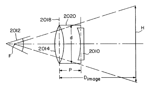
;~ V. O~tics For Head-Mounted System
A preferred embodiment of the invention is
illu~trated in the direct view, helmet mounted display
~y~tem of Figure 32. An active matrix single crystal
silicon display device 2010 is mounted în close
proximity to the eye 2012. A lens 2014 is used to
deliver a focussed image to the eye. Lens 2014 has a
given thickness and a diameter d. Table 1 lists
characteristics of commercially available lenæ
25~ including diameter, F# and center thickness. Other
lenses haYing the desirèd dimensions are easily
manufactured to provide the thickness and focal length
necessary.
~ :
. ~ , ,
, .;, ~, ,
} ~
WO 93/1~28 PCT/US93/02312
2130(i72
- 64 -
Table 1
Nom. Nom.
Diam. f BFL Ctr. Edge
in. ~589nm QS89nm Thk~ Thk.
( ) (mm) (mm) F/# (mm) (mm)
_____________________________________________________
O.S 11 9 0.8 5.7 1.34
(12.7) 13.7 12.2 1.0 4.3 1.1
16.6 15.4 1.3 3.6 1.1
20.5 19.5 l.S 3.1 1.1
26.4 25.6 2.0 2.6 1.1
38.4 37.7 3.0 2.1 1.1
51.3 50.7 4.0 2.0 1.2
1.0 20 18 0.8 11.0 2.3
lS (25.4) 27.4 24.6 1.0 8.2 1.8
33 30.7 1.3 6.7 1.6
39 37 l.S 5.8 1.6
51.7 50.2 2.0 4.7 1.6
63.6 62.3 2.5 4.0 1.6
76.6 75.2 3.0 4.0 1.9
101.6 100.3 4.0 4.0 2.4
l.S 34.4 29.4 ~.85 14.0 1.9
(38.1) 40 36 1.0 ~2.0 2.1
52.5 4g.4 1.3` 9.1 2.0
64.2 61.7 1.7 7.5 1.8
77 74.8 2.0 6.5 1.8
101.8 100 2.6 5.3 1.8
127.2 12S.~6 3.3 5.0 2.2
2.0 42 34.2 0.8 21.0 2.4
! ; 30 (50.8) 53.6 48.4 1.0 lS .0 2.0
61 1.2 12.0 1.7
77.8 74 1.5 11.0 2.6
102 100 2.0 8.3 2.0
127.6 125.3 2.5 7.0 2.0
176.5 174.4 3.5 6.4 2.8
, ~:
~- ~
~ ~ , . . . . .
WO93/l84~ PCT/USs3/02312
2l~n~72
-6s-
The distance from the center axis 2018 of lens
2014 to the display 2010 is denoted by P. The active
~atrix display has a high pixel density so as to match
the resolution of the human eye. 8y incre~asing the
resolution, or the density of pixels in the active
matrix display 2010, and at the ~ame time reduce the
size of the display it is possible to position the
display closer to the eye.
Where the distance P is Iess than 2.5 centimeters,
the pixel density is at least 200 lines per centimeter
and preferably over 400 lines per centimeter to provide
the desired resolution.
Where P=1.5 centimeters, the display 10 is about
1.27 centimeters in diameter and has a pixel density of
about 400 lines per centimeter. The focal length FL
bet w en the lens 2014 and focal point F is generally
defined by the Expression:
+
FL P D~aE
Solving for the distance to the image we obtain
D~g~ ( F~, P)
As the human eye will optimally focus an image at
a distance of about 400 centimeters (about 15 feet),
and as t~e focal length of the lens is preferably small
enough to focus the image onto the eye over a short
distance, the diameter of the lens should be less than
3 centimeters and preferably under 2.0 centimeters.
~,
WO93/18428 PCTlUS93/02312
2130~72
-66-
Table 2 defines the relationship between lens
diameter d, and the distance between the lens and the
display P in accordance with the invention where D~aE
is about 400 centimeters:
Table 2
Lens Diameter d Obiect Distance P (all in cm)
0.6 0.48
0.8 0.64
1 0.80
1.2 0.96
1.4 1.12
1.6 1.28
1.8 1.43
2 1.59
2.2 1.75
` 2.4 1.91
2.6 2.07
~ ~2.8 2.23
- - 3 2.39
:
The above summarizes the preferred element~ of a
head unted display where the active matrix display
and lens Qstem are mounted in close proximity to the
eye. Note that the lens need not be circular in shape,
however, but can be of a different shape to provide
more peripheral information to the eye.
The following embodiment comprises a simple
- i optical approach to attain a brightness increase of up
to 100% by reducing a common parasitic loss. This loss
obtain~ in all liguid crystal display light valves at
the first polarizing filter, which attenuates one half
of the unpolarized light emanating from the lamp. In
,
"
WOg3/l84~ '~ 2 PCT/USg3/02312
-67-
other words, the light source of the display generates
light of two polarizations; one polarization (half of
the light) is absorbed by the polarizing filter to make
it suit~ble for modulation by the liquid~crystal.
In this embodiment, as shown in Figure 33, the
light from source 30 is polarized, not by a polarizing
filter, but by a Brewster polarizing window 2032 which
passes one polarization 2033 only to light valve 2036.
The other polarization 2034 is reflected, at window
2032 and reflected again at mirror 2037 and directed to
a second light valve 2038. There are at least two
implementations of this invention, as follows:
In a head-mounted display the Brewster window 2032
can be u~ed to pass polarized light, TE polarized for
ex~ple, to the right eye 2035 light valve liquid
crystal display 2036. The reflected light, TM
polarized in this example, is passed to the left eye
` 2039 light valve liquid crystal display 2038. Neither
light valve requires a ~first" polarizer, although the
20 presence of one introduces only a slight reduction in
fluence since the light is already polarized. -Thus,
- ub~tantially'all of the incident light iæ passed to
the liquid crystal, leading to near doubling of the
optical efficiency. Of course, the liquid crystal in
the left and right liquid crystal display must be
rotated 90 with respect to each other to account for
; the polarization of the ~E and TM polarizations of the
light. i me absence of a "first" polarizing filter can
reduce the cost of the display.
Another preferred embodiment of the invention is
illustrated in Figure 34. In this embodiment the
active matrix 2050 is fabricated where the pixel
geometry and pixel area is variable as a function of
~ WO ~3/lU~ PCT/US93/02312
~13~72
-68-
the position of the pixel wit~in the matrix. This
provides a wide angle field of view image tbat can be
projected onto the internal surface of th,e face shield
2054 of the head mounted di~play. This ~i~ual èffect
S can also be done electronically by transforming the
video input such that the intensity of appropriate
pixels is adjusted to conform to the viewer'~
perception. The eye tracking system described
previously can be used to adjust intensity depending
upon the direction in which each eye is looking.
Figure 35 illustrates a detailed view of a portion
of the active matrix surface area. Pixels 2060, 2062,
2064 and 2068 have an increasing surface area as the
distance from the pixel to the matrix center 2066 axis
is incre~sed. The distance between adjacent column
lines and between adjacent row lines also increases as
a function of the distance from center axis 2066. The
matrix can be a backlit transmission display or an
emission type display. The activè matrix can be formed
on a first substrate and transferred onto ei~her a flat
or curved substrate prior to mounting onto the optical
support assembly of the helmet. The active matrix can
also be transferred to a flat substrate that is
subjected to a low temperature anneal in the range of
2S 300-400F and preferably at about 350~ that will
provide a desired curvature to the active matrix.
A further embodiment is illustrated in Figure 36
wherein separate active matrix display elements 2070,
2072, 2074 etc. are mounted or tiled onto a plastic
visor ~creen 2076. The visor screen can be
polycarbonate, polyethylene or polyester material.
Each~display element 2070, 2072, 2074 can have driver
~* g3/184~ PCT/US93/02312
213~2
-69-
eireuitry 2082, 2080, 2078, respeetively, formed
separately on the edge.
Figures 37A-37C il~!strate other pre~erred
embodiments of a direet-view display syst~em. Light
from a display deviee 1610 is represented by light ray
1615. The light ray 1615 from the display 1610 may
pass through an optical system or lens 1620. The ray
of light 1615 from the display 1610 is eombined with
ambient light 1690 before beeoming ineident on a
viewer's eye 1600. Thus, the image ereated by the
display deviee 1610 appears to the viewer to float in
the viewer's field of vision.
There are various means of combining the display
image 1615 with the ambient image 1690, whieh will now
be deseribed. Figure 37A illustrates a preferred
embodiment of the invention using a prism 1710 to
combine the images. The hypotenuse of the prism may be
eoated with a partial refleetor or electroehromatie
material 1712 to attenuate ambient light 1690. Figure
37B illustrates a preferred embodiment of the invention
u~ing a lentieular strueture 1720 as an image eombiner.
The gradings are spaeed euch that the eye 1600 eannot
distinguish lines in the structure 1620. In a
preferred embodiment, the grating density is greater
than or equal to 150 per ineh. Fîgure 37C is similar
to the lenticular structure in Figure 37B exeept that a
Fresnel lentieular strueture 1730 is used. In both
! I lentieular struetures 1720, 1730, the flat surfaee
1722, 1732 may also be eoated with a partial reflector
or eleetroehromatic material. In either of Figures
37A-37C, the display system 1610 may be mounted
dj~eent to the viewer~s head. In a preferred
-bodiment of the invention, the display device 1610 is
WOg3/18428 PCT/US93/02312~
S 7 2
-70-
mounted adjacent to the sides of the viewer's head,
such as on the sides of a viewer. The head mounted
~ystems described herein utilize audio cir,cuitry and
acoustic speakers to deliver sounds to t~e user's ears
and can employ sensor ~ystems such as cameras, magnetic
position sensors, LED's or ultrasound for determining
the position of the user's head. Additional sensors on
a user's glove or other actuators can be electronically
connected to a 8ystem data processor to provide
interactive capabilities.
Equivalents
The preceding description is particular to the
preferred embodiments and may be changed or modified
without 8ub5tantially changing the nature of the
~- 15 in~ ntion. For example, while the invention has been
illu-trated primarily by use of a passive ~ubstantially
tran8parent LCD display, other type displays both
active and pas8ive are within the contemplation of the
invention; 8uch as, without limitation, the f~ollowing:
-~ 20 aotive di~play8, e.g., plasma display panel8~
electrolumlne8cent displays, vacuum fluorescent
displays and light emitting diode displays; passive
di~plays: electrophoretic image di8plays, suspended
particle displays, twisting ball displays or
transparent ceramic displays. In each case, the eye
tracking~photodetector system can be formed in the same
film a8 the di8play pixel or monolithically formed
above or below the pixel to sense which pixel or group
of pixels receive eye reflected light. While the
30 inN~ ~tion ha~ been particularly shown and described
with~referenoe to preferred e bodiments thereof, it
wi1i~be~under-tood by those skill-d in the art that
~093/l84~ PCT/US93/02312
'~} 2130~S72
-71-
various changes in form and details may be made therein
without departing from the ~pirit and scope of the
invention as defined by the appended claims.
, :
:
~",