Note: Descriptions are shown in the official language in which they were submitted.
Wt~ 93118S79 ,~, ~~ :t~ .~ ~ ~ Pt.'T/US~3/01781
1
DESCRIPTION
VIDEO SIGNAL DATA AND COMPOSITE SYNCHRONIZATION
EXTRACTION CIRCUIT FOR ON-SCREEN DISPLAY
FIELD OF TFiEINVENTION
The invention relates generally to circuits for
recovering and processing certain portions of a video signal'
and relates particularly, but not exclusively, to the
extraction of timing and data information from a composite
vidoo signal for providing on-screen display of closed-caption
or text information.
BACKGROUND OF THE INVENTION
Television receiver regulations in the United States call
for future television receivers to be able to process signals
which contain information in encoded dat~c format within line
2~; of the scanned television raster, referred to as °'line 21
information, " :From which there may be generated a display of
closed captioning information (Federal Communications
Cammis ion Report and Order on~GEN Docket No: 91-1, dated
April 1.2, 1991); The data contained in raster line 2I may be
video related, in which case it is referred to as °'captions",
or non-video related, in ~rhich case it is referred to as
~~ text" .
In order for a television receiver to make use of the
line ~1 inf~rmation; it is necessary to locate the signal
portion representing raster line ~l containing the data, to
extract the data, to decode it, and to transform it into the
appropriate alphanumeric characters, which aye then
ineorgorated into the demodulated video signal for display, on
the screen. The proper recovery, identificatian, and placement
of the characters on the screen requires accurate tza~ing and
synchronization with the horizontal and vertical timing of the
composite video signal and therefore makes necessary a stable
timing reference and a highly accurate extraction of timing
W~ 93/18579 .. . PLI'/US93/01788
2
information from the incoming composite video signal.
Television video waveforms, called "composite video,"
contain horizontal, vertical, and field synchronization
information, along with the picture information. FIG. 1 is an
example of such a composite video signal. The synchronization
information portion of the waveform, which includes both
horizontal and vertical synchronization is referred to as
"composite synchronization." A schematic example of a
horizontal interval waveform 11, labeled as such, is
illustrated in greater detail in FIG. la.
A serious difficulty in the extraction of composite
synchronization from a composite video signal is that such
signals as are availalale in a television receiver frequently
contain considerable extraneous noise, particularly impulse
noise. In addition, the signal amplitudes may vary widely. A
receiver system which is able to respond properly to such
varying amplitudes is referred to as being "adaptive."
The composite synchronization can be extracted from the
composite video by means of a voltage clamping circuit, or
"clamp"; and a voltage comparator. The most negative part of
the video waveform, referred to as the "synchronization tip",
Qr "sync tip" is caused by appropriate electronic circuits to
be set, or °'clamped" to a reference voltage, so that all of
the synchronization tips, or at least'th~ average voltage of
the synchronization tips in the case of-a n~isy signal, are
set to this clamp~,ng voltage level shown in FIG. 1b in
relation 'to other vo~.tage features of the signal. ~ second
reference is chosen to be at a higher voltage than the
clamping voltage and preferably at a level exactly halfway
between the clamping level and the level of the back porch
ve~lt~ge. This second voltage level is called the "slice
leuel~." If the videfl.waveform is applied to the positive input
of a voltage comparator and the slice level voltage is applied
to the negative input of the voltage comparator, as shown in
Figu=e lc, then whenever the video wav~form voltage is more
positive than the~slice level, a positive voltage appears at
the output of the comparator. Conversely, when the video
i~O 93/ 1 X579 PCT/LJS93/01781
I.a ~ ~4~1J~~,~
3
waveform voltage is more negative than the slice level, a
negative voltage appears at the output of the comparator. The
resulting output of the comparator is a "squared-up" version
of the lower portion of the video waveform and is what is
considered the composite synchronization, as shown in Figure
1d.
While the timing signal pulses normally are easily
distinguished by the comparator from the remainder of the
composite video signal, this process is vulnerable to signals
with noise added. Additional difficulties with existing video
signal timing extraction circuits which are addressed by the
present invention will also be discussed below>
The extraction of the data which has been encoded into
the television raster line ~1 requires several operations.
Typically, a~.ong with the data itself, there is also included
information about the :ait, or clock rate and the byte
boundaries. The recovery process requires that the internal
clock be synchronized to the transmitted bit rate, that the
tl.ming of the byte boundaries be established, and that the
proper slicing level b~ set to enable the recovery of data
even under adverse conditions of signal level deterioration
and noise. The synchror~iaation of the internal clock timing to
the transmitted bit rate clock timing constitutes a timing
recovery process referred to as '°data clock recovery". The two
clocks are usually at the same frequency, but they must be
brought a.nto a mutual phase lock condlaion, so that the
extraction circuits can sample the sliced data at the optimum
time to achieve the optimum data reoovery in a noisy
environment.
The video signal input to the data recovery circuits is
usually already clamped by the grevious circuit action. The
establishing of the slice level for use in th~ voltage
comparator for extracting the data is more diff~.cult than it
i~ in the synchronization recovery process, however, because
the data occurs infrequently, once per television frame, and
for only short periods of time during line 2l. Good data
recovery depends on an adaptive data slice level which can
WO 93118579 PCT/US93l~Dt7~l
adjust quickly to variations in data amplitude in a given line
21 while also being able to hold the slice level between
successive frames. Although circuits have been devised which
perform these functions, the additional requirement that such
a circuit perform well within an integrated CMOS environment
adds serious complications. There is a need for a sample-and-
hold circuit which performs all the needed functions without
the need for components external to the circuit chip which are
normally required.
The internal timing signals needed to perform all of the
processing for data recovery and display, also referred to as
the video "dot clock," are derived from a single, stable, high
frequency timing source reference. This stable timing
reference is normally a VCO (voltage-controlled oscillator)
whose frequency is established by a crystal or by other stable
discrete components and which is then phase-locked to the
composite video synchronization signal. This timing reference
1.s used in the data extraction phase and also in generating
fitter-free characters for display. The requirements for
achieving Such a stable VCO are easily met in a discrete
environmento but are usually difficult to achieve in an
integrated circuit whose designing involved the primary
objectives of minimum size and minimum number of lead
connections: There is therefore a need for a circuit which
provides the required VCO performance within a CMOS
environment.
SUMMARY 0~' THE INVEIrITION
The novel extraction circuit in accordance with the
present invention includes the following features;
"A novel means i:s provided for generating a stable timing
reference using a minimum number of external terminals and.
reguiring only relatively ion-critical components to
a.c~curately establish the operating frequency.
The basic VCO is implemented by means of a simple ring
oscillator consisting Qf an odd number of invert~.ng stages and
using no external components. In a CMOS environment, the
PCT/US93/1~17~1
WO 9311 X579 . .
fundamental aperating frequency is determined by the number of
stages in the ring and the propagation delay of each stage.
This results in a minimum configuration implementation.
However, the operating frequency is not precisely determined.
The VGO is brought into the desired operating frequency range
by a frequency steering circuit which comgares the divided VCO
frequency to a second timing signal which is approximately
equal to the horizontal timing of the input composite video.
This second timing signal may be supplied from the outside
(off-chip) or generated internally (on-chip), either by
hardware or by software, using the on-board cpu (central
processor unit).
The divided VCO signal is part of an internal timing
pulse generator chain which produces outputs locked in phase
to both the horizontal and vertical timing signals of the
incoming video signal. These noise-free "flywheel'° timing
signals are used as the source of timing information for the
remainder of the circu~~t, thus virtually eliminating the
effects of noise in the input signal. The °'loek" to the
vertical timing is essential to finding the raster line
portion of the television signal containing the data and also
pro~r.~des a novel ability to detect a change in the television
channel without having available a signal from the receiver°s
tuner circuits:
A dual clamp system incorporating a superior diode clamp
for initially clamping the synchronization level and then
switching to a Gated Clamp provides good noise immunity.
proper startup of the circuit is assured by the use of a first
clamp which is indegend~nt of timing information for its
operation, but wh.ieh is sub~eet to noise, and subsequent
switching to a second clamp which is dependent upon timing
information as derived with the use of the first clamp, bu-~
which is substantially immune to noise.
A novel means establishes an adaptive synchronization
slice level with high no~.se immunity, using a stable "times 2°'
amplifier. The extraction of the timing signal is controlled
by a novel slicing circuit in which the input signal is
i~0 93!18579 PCT/US931~1781
:ice ~. J 1 6
sampled at the back porch voltage level and this level is then
compared to the composite video signal, which has been doubled
in amplitude. This guarantees the establishment of the slice
level at the middle of the synchronization amplitude,
independently of the input amplitude.
A novel data recovery system uses a closed-loop digital
phase adjustment technique for clock recovery and a sample-
and-hold technique for establishing the slice level. The data
slice Level reference voltage establishing and retaining
circuit makes use of a combination of a digital encoder and
decoder in conjunction with a voltage comparator to eliminate -Y
the need for a large, high quality, off-chip capacitor. Such a
capacitor would contribute to leakage problems, due to the low
duty cycle nature of the signal.
These and other features of the invention will be
discussed below in more detail.
BRIEF DESCRIPTION OF THE DRAWID1GS
FIGURES l through ~.d are exaggerated, schematic prior art
representations of various aspects of waveforms of a composite
video transmission signal in various stages of signal
processing.
FIGURE !e is a schematic representation of the signal
waveform of the raster line 21.
FIGURE 2 is a circuit diagram in block form of composite
video signal processing circuits for timing and data
ektraction and processing in accordance with one embodiment of
the invention.
FIGURE 3 is a schematic circuit diagram of a diode
clanging circuit of the type found in the prior art.
FIGURE 3a is a schematic circuit diagram of a gated
c~.amping circuit of the type found in the prior art.
FTGURE 3b is a timing diagram describing the operating
characteristLcs of the gated clamping circuit of FIG. 3a.
FIGURE 3c is a schematic circuit diagram of a noel gated
clamping circuit useful in the circuit of FIG. 2.
FIGURE 4 is a schematic circuit diagram of a novel
Vll~ 93/8579 PCT/US93/01781
:~: i ~ ..
:.~ ~ ~y, s,.
7
reference voltage clamping circuit of the circuit of FIG. 2,
FIGURE 5 is a schematic representation of a novel dual-
mode clamping circuit useful in the circuit of FIG. 2.
FIGURE 6a is a schematic circuit diagram of a novel
synchronization slicer useful in the circuit of FIG. 2.
FIGURE 6b is a schematic representation of another, dual-
mode synchronization sliver alsa useful in the circuit of FIG.
a.
FIGURES 6c and 6d are diagrammatic representations of a
clamped video and gain-of-two amplifier of the circuit of FIG.
2, showing slice voltage levels.
FIGURE 7a is a diagrammatic prior art representation of a
line 21 video waveform, showing the data slice voltage level.
FIGURE ~b is a diagrammatic representation of the line 21
video waveform of FIG. 7a~ showing also the gate timing for
the novel data slice circuit.
FIGURE 7c as ~ schematic circuit diagram of a prior art
data slicing circuit.
FTGURE 7d is a schematic circuit diagram of a novel data
slieruseful in the circuit of FIG. 2.
FIGURE 8 is a schematic circuit diagram, in block farm,
of a novel data clock recovery circuit of the circuit of FIG.
FIGURE 9 is a schematic circuit diagram; in block form,
of a novel phase and frequency locking circuit of the circuit
of'FI~: 2.
FIGURE 10 is a schematic circuit diagram, partially in
block form, of a novel vertical pulse detection and countdown
synchronization circuit of the circuit of FIG. 2.
DETAILED DESCRIPTI(7N
Tn order to facilitate the below discussion, reference is
made to FIGS. l and la of the drawings. There is shown in
FIG: la a.pictorial representation of that portion of a
comp~site video signal 1a1 representing a s~.a~gle horizontal
line. Tt begins with a horizontal synchronization pulse 1a2
including the front and back porches appearing below a black
1~~ 93/18579 a:., .~ u~ ~ ~ ~ ~ PCffUS93/01781
8
level voltage 1a3. The interval above the horizontal
synchronization,pulse 1a2 represents the horizontal blanking
interval 1a3. The voltage level at the upper right-hand
shoulder of the horizontal synchronization pulse 1a2 is
referred to as the "back-porch" voltage level 1a4. After the
horizontal synchronization pulse 1a2, comes a color burst lay
for color synchronization, followed by the video content
portion in the form of both luminance and color information in
an overlay as a composite signal la6r
The various features of video signals themselves, as well
as the structual nature and operating characteristics of
circuitry for receiving them, including extraction circuits,
are by now well known in the art for both vacuum tube and
transistor technologies. Therefore, the specifics of such
known circuits will not be needlessly discussed. Moreover,
since modern integrated circuits are largely designei3 in
functional subcircuit cell form with the internal hardware
details being provided by means of CAD (computer assisted
design) systems, the circuits herein will be represented
largely in functi~nal.block form. However, where novel
circuit features are irwolved, such features will be
pa=ticui:larized to the extent considered necessary for
permitting a person skilled in the art to adapt them for use
in a suitable circuit for practicing the present invention.
Referring now to FIG: l, that portion of the signal which
encompasses raster lines l through 21 constitutes the vertical
blanking interval. Two fields comprise a complete frame. The
odd field is defined es the field wlhich begins on a horizontal
l~~e ba~n~~,~r, while the even field starts in the middle of a
horizontal line. The vertical blanking interval starts with
thr~:e horizontal line periods of synchronization pulsee at
twice~the normal horizontal rate, called the "pre-equalizing'°
pulses. This is followed by another three-ho~.a.zontal-line
period of broad pulse. with synchronizing serrati~ns, called
the "vertical pulse period". The following l:h~ee-h~xizontal-
line period also contains 2h synchronization pulses called the
"post-equalizing pulses". The remainder of the vertical
WO 93/13579 PCT/115931~Dt781
,'s
':I iy A
~l ~ ~ ~~ EJ G.I
9
blanking interval consists of normal horizontal
synchronization pulse periods which do not contain any video
picture information. The last line of the vertical blanking
interval in the odd field is line 21. In the even field, only
the first half of line 21 is within the vertical blanking
interval.
Fig 1e shows the closed captioning waveform normally
transmitted within line 21 of the odd field. Following the
standard horizontal synchronizing interval and the color burst
is a period of seven clock cycles, a period of zero level, and
then a period of 17 pulses at twice the rate of the seven
clock pulses. The first of these 17 pulses is always present,
but the remaining 16 pulses are transmitted as two eight bit
data bytes using the ASCII code, with odd parity for the data
desired.
It need hardly be stated that such video signals and
various types of circuit hardware for extracting information
from them are by now well known in the art for both vacuum
tube and transistor technologies. Therefore, the specifics of
such known circuits need not be discussed, and the circuits
will b~ represented'trerea.n largely in functional block form.
However, where novel circuit features ale involved, such
features will be particularized to the extent considered
necessary for permitting a person skilled in the art to adapt
them for use in a suitable tircuit for practicing the present
invention.
~~~~~~ CIRCUIT FE~~ux~s
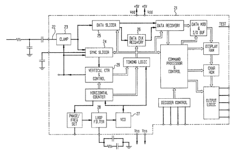
Figure 2 shows in signal flowchart form the architecture
of a video signal timing and data recovery and processing
circuit 2l in accordance with one embodiment of the invention.
Ah 3:mportant practical aspect of the circuit 21 which should
b~ noted is that it is particularly well. suited for
realization in CMOS (COMPLEMENTARY METAL°OXIT3E°SEMICONL1UCTOR)
t~cha~ology. This ~.s of special significance because the nature
of the task of decoding the captioning data in the video
signal and generating the corresponding characters for display
W~ 93/18579 ~~ ~ ,~..~,f j.~' ~ PCTlUS93/017~1
IO
on the screen calls for both analog and digital processing
functions. The digital functions are best carried out by a
CMOS device. By making the analog functions also realizable in
this technology, the entire set of functions may then be
incorporated in a single integrated circuit chip, thus
significantly reducing the cost, size, and power requirements.
In this regard, CMOS technology presents some particularly
challenging practical problems. There are relatively wide
variations in the values associated with individual components
from wafer-to-wafer in the CMOS manufacturing process. In
order to accommodate such variations, the novel extraction
circuit 22 includes a number of sub-circuits especially
adapted to the GMOS environment, but also capable of being
adapted for applications in other technologies.
Most transistors referred to below are in the farm of
complementary pairs, as is well understood in the CMOS design
art. Conventional symbols are used to indicate whether they
are P-type or N°typ~ conduction channel devices. P-type
devices have their source on the positive voltage side, while
N-type devices have th~ir source on the negative voltage side.
,once the drawings show the interconnection of the devices in
a manner which would make-the realization of the circuits
readily apparent to'one skilled in the art; such connections
w3:11 z~ot be further cataloged in detail, but will instead be
d.iscu~~ed functionally: Reference to a transistor being ,
connected "between" two points means,that the source and drain
are connected to the p~ints as appropriate, taking into
consideration the conduction channel type of the transistor.
of particular' interest in the circuit 23 of FIG. 2 are
tie video input node 22 and the functional blocks identified
as the CLAMP 23, the SYNC SLICER 24, the DATA SLICER 25, the
DATA CLOCK RECOVERY 26~ the VCO 27 and LOOP FTLTER 28, and the
VERTICAL CUUNTER AND CONTROL 29, and the .. Ln accordance with
t~~ present invention, the functions of these blocks are
provided by means of novel circuits as discussed below in
terms of functional caitegories .
WO 93!18579 PCT/US93/fl1781
3 ~~ ~~.~ ~_; ~.
I 1 ~ ~.
DIODE CLAMP
Referring again to FIG.2, the first function to be
performed on the signal 21 by the extraction circuit 21 is to
clamp the voltage to approximately I volt above ground
potential by a clamp 23. "Ground potential" in this context
means a reference voltage in the circuit 21 which is nominally
at 0 volts, and does not necessarily mean earth ground
potential of the associated equipment. The clamping function
is normally carried out in the prior art by a diode clamp 31
and resistor 32 as shown in FIG. 3. The diode clamp 3I
consists of a capacitor 33 having an input side 34 connected
to the incoming signal, while the other side 35 is connected
to a d.c. (direct current) restoring resistor 32 and is also
connected to the clamping voltage Vclamp by a reverse polarity
diode 36. It can be seem that the clamped video node 37 of the
capacitor 33, which is the video output, will be maintained by
the diode 36 at the clamping potential, which is at a level
below Vclamp by reason of the voltage drop across the diode
36:
ItEFERE~ICE VOLTAGE CLAMP
One problem associated with the prior art diode clamp is
that CMt3S technology does not lend itself to the formation of
d~.odes in the circuit. A second is that the current capability
of diodes is more limited than would be desirable for the
response tame needed at the node 37 for this application. A
th3.rd is that diodes genex'ally have temperature-dependent
forward current charac~Geristics and leakage current. The
effect of such temgex'ature dependence ~f the charging and
discharging currents of the composite synchronization node 37
can resul~'in output signal distortion by changing the slope
of the edges of the composite synchronization output signal.
In order to address the above-remaining prob7lems
asg~oaated with the clamping functions there is provided in
the extraction circuit 21 a novel form of fiche clamp 23, the
function of which is similar to that ~f a diode clamp. The
novel clamp is shown as clamp 41 in a schematic diagram of the
IVVO 93/1857 ; :~, ; ~~ PCI'/US~3/a1781
:a ~.'. :.r ~.l .)
12
circuit of the clamp in FIG. 4. The circuit will be referred
to as a Reference Voltage Clamp, or "RVC". The clamp 41 also
features a capacitor 42 and a composite video output node 43,
similar to that of the above-referenced diode clamp 31 of FIG.
3a. However, instead of a diode, there is provided a charging
current source 44 and a P-type charging transistor 38
connected in series between 'the output side of the capacitor
42 and a positive voltage rail V+. A comparator 46 has its
positive input connected to the output node 43, its negative
input connected to the clamping voltage Vc, and its output
connected to the gate of the transistor 45. A second
discharging current source 47 is connected between the node 43
and ground potential.' It can be seen that in operation,
discharging current source 46 draws the node 43 down in
voltage by discharging the capacitor 42 until the voltage on
node 43 is lower in voltage than the clamping voltage Vc. When
the video syrachron.ization tips are lower in voltage than the
clampaa~g voltac3e Vc by an amount that is greater than the
threshold of the moltage comparator 46, then the comparator 46
out~aut changes state and applies to the gate of the P-type
trans3:s~.or 45 a voltage to turn it on and bring the voltage of
the node 43 back up to the clamping voltage Vc. The charging
current s~urce 44 has a current capacity which is greater than
that of the discharging;current source 46 by the factor of the
'inverse r~tfo of the synchronization tip time duration to the
horiz~ntal 1'a.ne time and draws the video line up in voltage,
overcoming the effects of the discharging current source 46
and charging the capacitor 42 until the voltage of the node 43
is greater than the clamping voltage Vc, thus changing the
state of the voltage comparator 46 to turn bff again the
transistorr45. This permits the discharging current source 46
to draw-the node 43 down again to repeat the process. As
integrated o~rer time, this process clamps the video
synchxonizati~n tips to the clamping voltage Vc.
The advantages of the above novel CM~5 Clamping
arrangement are that 1. It does not require a diode; 2. It
does not draw current from the clamping ~roltage reference; 3.
~V~ 93/~~579 ' % ~-' ~~ ~ ~ ~ PtT/US93J017~7
s~ ~,. ~>
13
The clamping voltage differential is small, essentially the
input threshold of the voltage comparator; 4. Only very small
temperature effects are present; and, 5. The current carrying
capability of the current sources 44 and 46 and the transistr°
45 are relatively high, thus permitting a fast response time.
Additionally, the current sources 44 and 46 may readily be
constructed to offer temperature-compensated operation.
TMPROVED GATED CLAMP
Tt is desirable that the clamping function be relatively
immune to the imperfections in the video waveform caused by
noise in the video signal. One way to imgrove such immunity is
to limit the operation of the clamp to only intervals during
which the synchronization pulse is present. This can be
achieved by means of an electronic switch which is enabled at
the horizontal synchronization rate by the synchronization tip
gate pulses, as is the case for the prior art Gated Clamp
circdit 3a1 of ~'IG. 3awhich has its operation related to the
signal timing as is illustrated graphically in FTG. 3b. The
Gated Clamp 3a1. works on the principle that a "gate" pulse,
derived from the synchronized clock, having the proper width
and-position in time is applied to an electronic switch 3a2
placed'-between the reference voltage Vc and the clamped video
output lead 3a3: When the synchronization tip is present and
the switch 3a2 is classed via the gating pulse, and if the
video synchronization tig voltage is different from the
reference voltage Vc, an adjustment current will flow to or
from the reference voltage source V.to adjust the charge on
the capacitor 3a4 through the video source. When the capacitor
3a2 zs sufficiently charged, which process mad require the
pissing of several synchronization tips, the video
synchronization tip will be essentially at the same value as
the reference voltage 'asd is then considered to be clamped to
the reference voltage. between synchronization tip gate
pulses, the clamped video lead will essentially "float," and
'the capacitor 3a2 will charge or discharge, depending upon
several factors. The capacitor 3a2 charge will be restored by
WO 93/1H579 PCF/US93/017~I
~:~x~~~;;~~,
14
succeeding synchronization tip pulses.
The Gated Clamp circuit 3a1 can fail to operate properly with
video signals that have anomalies in the horizontal and/or
vertical synchronization pulses. For example, there may be
missing pulses in non-standard video or during high impulse
noise conditions. Also, the synchronization pulses may be
displaced in time by VCR tape stretching. In ary case, if the
synchronization tip is not present when the gate pulse
arrives, then the circuit will attempt to clamp at an
erroneous video level. The novel circuit of the improved Gated
Clamp 3c1 shown in FIG 3c eliminates the erroneous clamping
action without sacrificing the other advantages of a gated
clamp. This improvement is accomplished by AND'ing the gate
pulse with the composite synchronization pulse in the AND gate
3c2. This enables the switch 3c3 at the proper time, only if
the synchronisation pulse will be sampled, thus insuring that
an erroneous level can never be sampled.
DUAL NIOI?E CLAMP
A problem arises w~.~h the above Gated Clamp 3a1 in that
it'tnay not start up properly, since composite synchronization
is needed to obtain the synchronizatian tip gates and since
proper clamping and slicing are needed ~to obtain the composite
synchronization. This problem is eliminated by the
introduction of a novel dual-mode system for the clamp 23 of
FIG. 2 which includes both an RVC clamp for starting up
independently of the timing information and an. improved Gated
Clamp which is switched in to replace the functa.on of the RVC
clamp after start--up, arhen there is sufficient timing
information to supply the appropriate slrnchronization tip
gates for operating the. gate switch.
FIG 5 depicts the', novel dual-mode clamp 52. Composite
video is fed to the circuit via a capacitor 52'and is clamped
to the clamping voltage Vclamp via a Reference Voltage Clamp
53,through electronic switch 54 and provides clamped video for
~~grial processing. When synchronization is acquired and
acknowledged, a s~ritch control 55 causes the switch 54 to open
WO 93/18579 ~ ~. ~ ~ :;~ ~ ~; P~'T/1JS93fO1781
1. 5
and the switch 56 to close, thus causing the Gated Clamp 57 to
operate.
The switching actions shown in figure 5 are actually
actions performed by means of CMOS digital logic.
SYNCHRONIZATION SLICER
In prior art arrangements, the composite video signal is
clamped to the clamp voltage ~Tc and applied to one input of a
comparator, such as was described in the context of FIG. lc.
The slice level voltage is applied to the other input of the
comparator. If the video sa.gnal is a standard video signal of
unvarying amplitude, then a fixed d.c. slice level voltage
equal to the average value of the synchronization tip and
porch levels is used. The composite synchronization appears at
the output of the comparator.
An alternate method, called an adaptive synchronization
e1ieet, is used in prior art circuits for a video signal which
varies 3n amplitude. Tn an the~adaptive dicer, the
sy~,~hron.ization tip and the parch voltages are separately
sampled, the difference between them is halved and added to
the synchronizati~n tip voltage, thus creating an average
value synchronization slice voltage which adapts according to
the w~.deo, or synchronization ta.p amplitude.
IMPROVED SYNCHiZONIZATION SLICER
schematic of ~n improved synchronization e1ieet 24 of
the circuit 21 of FIG. 2 is the sliest Gal shown in F'IG. 6a.
As prev3.ously noted with regard to the prior art
synchronization e1ieet, there the adaptive slice level voltage
was obtained by finding the synchronization tip voltage
peak'-to-peak amplitude, or synchronization tip height, halving
i ,.and adding it to the synchronization tip voltage level,.
The main feature of the improved synchronization e1ieet 6a1 is
that instead of halving the synchronization tip height, the
full, synchronization tip height is used as the slice voltage
level for one input to the synchronization dicer, and double
the amplitude of the clamped video voltage is used for the
WO 93!18579 ~ PCT/US93/01?8i
H: ~- ~'
16
second input of the synchronization slicer.
The clamped video and the double amplitude clamped video
voltage relationships are depicted in FIG. 6c and 6d. It is
important to note that the slicer 6a1 is configured such that
the synchronization tips of both the clamped video 6a2 and the
double amplitude clamped video 6a3 are at the same clamped
d.c. level, Vclamp. This result can be achieved by various
means. The method shown in FIG. 6a is that where the voltage
divider formed by resistors 6a4 and 6a5 for setting the gain
of the operational amplifier 6a6 and comparator ~a7 is
returned to Vclamp. The voltage divider 6a4,sa5 is used to set
the gain of the amplifier 6a6 to precisely two.
The slice level is obtained by sampling and holding the
back porch voltage level of clamped video node 6a2 with the
Gated Clamp 6a8, controlled by porch gate 6a9, charging and
storing the voltage level in capacitor fial0. This voltage is
applied to one input of the synchronization slice comparator
6a? and the clamped double amplitude video is applied to the
secand input: The composite synchronization is obtained at the
output: 6a11 of the comparator 6a?.
DUAL--MODE SY1~1CHRONIZATI~N SLICER
As is the case for the dual-made clamp 51, the slicer 24
of the circ~zit 31 of FIG. 2 is a preferably a dual-mode
device, shown as the dicer 6b1 in FIG. 6b. It starts in an
inferior mode and switches to a superior mode once
synchronization has been acquired. The circuits Gal of FIG.6a
anei 5b1 of FIG. sbare similar, except that the circuit 6b1 in
FIG. 6b uses a slice level 6b2 which is delta V above Vclamp
for Mart-up. Delta V is a voltage approximately equal to the
lowest expected input video synchronization tip heigrit, c3nce
synchronization is acquired, the lock control signal 6b3
causes switch 6b4 to connect the stored back porch level of
the clamped input video to one input of the voltage
comparator. The input signal 6b5 is amplified in an amplifier
6b6, with a fixed gain of two and applied to the other input of
the voltage comparato~ 6b?. The composite synchronization is
PC.TlUS93/U1781
WO 93118579 .: :: .. ,.
17
obtained at the output 6b8 of the comparator 5b7. The
advantage of this approach is that the slice level is placed
exactly in the center of the synchronization pulse by the
action of the gain of two amplifier, no matter what the signal
level. Furthermore, it is particularly advantageous that a
gain of two can be accurately established in a CMOS
environment.
DATA SLTCER
Data slicing is a pgocess whereby a digital form of data
is extracted from an analog signal upon which data has been
superimposed. For example, FIG. 7a shows a graphic
representation of line 2l of a video signal and the relative
timing of the run-in gate 7a1. FIG. 7c depicts a schematic of
a prior art circuit 7c1 by which the closed caption data can
be extracted from line 2l. Video is applied to one input of a
c~mparator 7c2 and a d.c. slice level ~.s applied to the second
input of the comparator ?c2,
In the c~.rcuat 7c1 shown in FIG. 7c, an electronic switch
?c3 connects the discrete component integrator R and C to the
video signal' during the run-in burst via the .run-in gate ?c4.
The output of the integrator R and C is a sample-and-hold
voltage of the average d.c. value of the run-in burst which
se~:~e~ a~ the above slice level.
gIG. 7d shows a novel circuit 7d1 useful as the DATA
SLIDER 25 ~.n the extraction circuit 21 of FIG. 2 for
pexfcr~l,ng the data slicing function. All he components shown
are pr~ducible in the CMOS technology. The component, i.a.
the electronic swit'ch'7d2, resistor ?d3. Capacitor ?d4, and
the comparatar ?d5 perform functions similar to those
corresponding components in the description for the cixcuit in
FIG.~7c: the holding switch ?d2 can be designed such that the
resistor ?d3 is a parameter of the switch ?d2.
The novel circuit ?dl, which includes a digital to analog
converter DAC and an analog to digital converter AI~C, solves a
problem which arises due to the low duty cycle and relatively
long sample-and-hold time in which the held charge can leak
1~~ 93! d 8579 PCTI US9310178 ~
~~_rii~V~~
1e
off the capacitor C, especially at elevated temperatures.
Another advantage is that the capacitor C is now incorporated
on the chip, thereby removing a costly external pin and
component and avoiding the leakage current associated with
external components.
The operation of the novel circuit 7d1 can be seen by
referring to FIG.is 7b and 7d. During the time when line 21
occurs, the circuit 7d1 operates as described in FIG. 7c,
except that the output of the DAC/ADC is disconnected from the
sample-and-hold capacitor C by means of the control gate
source 7d6 controlling the holding switch 7d2.
The remainder of the circuit 7d1 operates as previously
described. During line 22 (or any other reasonable time after
line 21) the DAC control source 7d8 operates, causing the
ADClDAC to samgle the voltage at the capacitor 7d4, causing
capacitor 7d4 to adjust its output to the nearest increment of
the output voltage of capacitor ?d4. After line 22 (or other
r~asonab7.e time) ~~e control source 7d8 turns off the ADC/DAG
ands~aitch 7d2 closes, applying the output 7d9 of the DAC to
the capacitor 7d4, which holds the charge for the remainder of
the video frame. The ADC/DAC, therefore, acts to supply
current to the capacitor ?d4 to offset any circuit leakage
current hat may be present during the interval from line 22
to the next Iine 21: Upon the arrival of the next line 21, the
ou'~~ut 7d9 of the ~,DC/DAC is disconnected from the capacitor
7d~, the'sample-and-hold operates to make a correction for
sfgnal level, if necessary and the process repeats.
In summary, In ~.he setting of the slue le~rel, of a small
slice level storage capacitor were used for the level holding
function, then its response to necessary adjustment would be
rapid. Howover, due to inevitable leakage of such a device, it
~rould~not be able to hold the slice level sufficiently
constant over such a long period of time as elapses between
ll:r~e 21 occurrences. The use of an external capacitor in the
CEO, ,implementation could roquire a very low leakago
component. Also terminal pins are at a premium and ire also a
source .of noise into the circuit. In addition each pin is
i~0 93/18579 ~ _~- ~~ ~ ~: ~ ~ PCTlUS931fl1781
19
connected to protection diodes which inevitably have
significant current leakage. This leakage leads a capacitor
connected to a pin to experience voltage "droop" during the
storage time interval. While the droop can be reduced by
increasing the capacitance value of this capacitor, thus
increasing the time constant, that would makes i~G difficult or
impossible to, then rapidly adjust the slice level during line
21, as would be required when code amplitude variations are
encountered.
The only error present with the use of the circuit 7d1 is
due to the granularity of the ADC. This may be determined in
advance with approp=fate design of the ADC to be less than the
required tolerance for the slice level. Because with the
circuit 7d1 the slice level capacitor 7d4 can be made very
small, it can be integrated on the chip and have a fast
response time while nevertheless holding the slice level
accurately to the degree desired. Any inaccuracy will be
adjusted for during tho next occurrence of line 21 run°in. It
is'raoted hat while the circuit 7d1 is in a sense highly
complex in terms of the number of active devices present in
the ABC and the DAC, and in this respect is quite different
from the type of circuit which has been traditionally used for
such a function in video c~.Lsuits, in the environment of a
COOS cixcuit, such complexity is readily available with little
added cyst to the integrated circuit chip because once the
cixcui~-bas been designed, the manufacturing cost is, within
limits, largely independent of the number of active devices
which are present im the circuit. Such an-approach to this
funct3.~an within the context of a television receiver circuit
is believed to be a significant departure from prior art
approaches.'
DATA CLOCK RECOVERY
Data clock recovery requires the internal generation of a
cl~ck signal which is used to sample incoming line 21 data
bibs at appropriate points away from data transition edges. In
the novel circuit 2l of the present invention, clock recovery
V (j ~j ~, ~. PtT/US93181781
WO 93/ 18579 ~~ "' ~' ~' ~ i~ ''
is achieved by using a closed loop digital phase adjustment
technique to control the phase of a 32H (32 times horizontal)
rate counter clocked by a signal which is frequency-locked to
the horizontal component of the input video waveform. This
novel technique eliminates several problems encountered in
previously implemented methods. Firstly, the technique
requires only easily implemented digital logic circuits,
eliminating the need for more complex analog phase locked loop
circuits. Secondly, the circuit performance in the presence of
noise on the input video waveform is enhanced by allowing the
phase position of the data clock to adapt more slowly than
would be practical in an analog phase-locked loop
implementation.
Referring to Fig. 8; there is shown a preferred version
of the DATA CLOCK RECOVERY 26 of the circuit 21 of FIG.,2 in
the form of circuit 81, in which the 32H signal is generated
by applying the video dot clock pulses, which are the output
of the VCO at nodes 82r to a 5 bit counting programmable
di~rider 83. This divider 83 is capable of dividing the clock
by 23, 24 or 25. A count of 24 produces the 32H clock. If the
div~:der ~3 is made to overflow at 23, then the ghasing of the
internal clock with respect to the clock run-in moves earlier
in the cycle. Lf the divider 83 is made to ove~°flow at 25, the
phasing of the internal data clock moves later in the run-in
cycle. This allaws the phase to be brought into lock with the
clock run--in within plus or minus one drat clock resolution.
Since only a resolution of approximately 3 dot clocks is
requi=ed for high performance operation, this l.i.mitation in
phase lock resolution does not degrade circuit performance.
The line 21, clock run-in component of the incoming
wweform is used as the phase reference for the internal data
clock. The phase steering to the data clock divider 83 is .
provl:ded by a phase comparison technique which produces a
binary error s3.gna1 indicating wheth~r the center of the
positive half-cycle of each of the clock run-~.n cycles is
lead~.ng or lagging the positive edge of the data clock. The
reference clock ~4 generates a 50~ duty cycle pulse train
P~.TlU~93/01781
I~VO 93/18579
-~u'_~~
::, ..~. -.a ~,
21
derived from the data clock divider 83 by decoding its rising
and falling edges. The lead/lag detect is accomplished with a
separate counting circuit 85 which counts on each video dot
clock, conditional on the presence of a 1 level on the data
input. This counting circuit 85 is forced to count up on dot
clocks before the rising edge of the reference clock and down
after the rising edge> The accumulated count at the falling
edge of the reference clock, i,e. either greater than 0 or
less thin 0, determines the phase steering for the next
reference clock cycle. This counting circuit 85 is cleared
synchronously with the failing edge of the reference clock to
prepare it for the next cycle. This phase steering process is
enabled only during the part of the line 21 waveform which
contains the clock run-in signal. At all other times the dot
clock divider $3 is set to a count of 24, which preserves its
phase in respect to tine clock run-in. This digital phase lock
eliminates the vCO dxoop end consequent loss of lock that
would occur between frames in a conventional analog phase
locked loop implementation: The data clock is then decoded
from the synchronized data clock divider by circuit 86. A
decod~,ng which leads the reference clock rising edge by
video dot clocks is used. The resulting data clock is ideally
positioned to sample the line 21 data. The reference clock
falling edge decode of the data clack divider 83 is logically
OR'd with the reference clock rising edge decode by circuit OR
circuit 87 to provide a'double rate clock for sampling of the
clock run-in and start bit to obtain the framing code bits.
vco Ar~r~ ~o~zzor~T~r., Loop
once the horizontal synchronization has been accurately
detected as described above, it becomes necessary to'
synchronize the internal timing signals to it in both
frequency and phase. In a first, common approach for
accomplishing the synchronizatioh, there is provided a high
frequency vCO which has its frequency set to the desired
center frequency of the signal. This signal is divided down to
horizontal synchronization signal frequency to permit a phase
!w0 93/18579 . ~ ~~ ~ ~ ~ pCT/US93/01781
»>
22
comparator to send a control voltage to the VCO to correct and
lock in the phase. Circuits which use digital phase/frequency
comparison techniques do not require very stable VCO's, but
the nature of the edge-triggered logic networks which perform
the phase and frequency steering result in very poor noise
immunity. In a second approach involving sampled-phase
comparator type circuits, there does result the desired noise
immunity capability, but such circuits require tight VCO
performance specifications and tend to produce static phase
error.
A much more serious difficulty with the above approach as
regards the extraction circuit 21 of FIG. 2 is that it is not
feasible in CMOS technology to provide an on-chip oscillator
with an accuracy anywhere near the 1~ which would be needed
for the VCO of the second approach described above. The
accuracy of CMOS oscillators is more in the range of 30~.
Therefore, a different and novel approach has been talon in
the circuit of FIG. 2 for accomplishing horizontal frequency
and phase locking.
Figure 9 is a block diagram of a novel implementation 91
of the VCO 27 and Fi LOOP 28 (Horizontah Loop) circuit portions
of he circuit ~1 of F'IG. 2 which does not require a stable
VCObut still provides good noise immunity, no static phase
error, and is easily implemented in a CMOS environment. The
circuit 91 starts out with a high frequency .lock at node 92
generated by a non-precision VCO. This clock is counted down
to pulses bf the same frequency as the horizontal frequency of
the video waveform and is held within precise freq~xency and
phase of the horizontal component of the input v~.deo waveform
by means of a PLL (phase-lock loop). This PLL utilizes a phase
comparator which has a high immunity to video waveform noise,
but suffers from a relatively narrow frequency pull-in range.
Pull-~in over a wider range is accomplished by the inclusion of
a parallel~connected frequency comparator wh3.ch steers the VCO
whenever the frequency of the counted down VCO output differs
from the frequency of an externally supplied referende
frequency by a fixed proportion. The frequency comparator
~V~ 93!18579 PCT/L1S93/01781
,err .
23
serves to hold the VGO frequency within a fairly narrow
window. When the VCO frequency is within this range, the
frequency comparator provides no steering of the loop. This
range is designed to be well within the pull-in range of the
phase comparator, which will then pull the VCO into precise
phase and frequency lock. It is important to note that the
externally supplied horizontal frequency reference at node 92,
typically a horizontal flyback signal in a television receiver
application, does not need to be precise in frequency or have
a known phase relationship to the input video signal. This
signal could typically vary by plus or minus 5~ without having
any effect on system performance.
Referring now to FIG. 9, the horizontal.frequency
comgarator 93 counts the number of divided VCO clocks received
from the Internal H Counter 94, which occur in a 16 video line
time window created by counting horizontal frequency reference
clocks. When the Reference Counter 95 has counted 16 reference
pulses, it sends a pulse to the frequency comparator 93 which
causes the state of ats frequency-down and frequency--up
c~ntrol signals at nodes 96;97 to be set for the next 16
reference pulse window. These control signals are set
dependent; on the count achieved by the Internal H Counter 94
at the time the Reference Counter 95 has reached a count of
16. If the low count, typically 14, has not been reached, the
fr~quenc~r-up signal i~ driven high, and the frequency-down
signal-is driven law for the next 16 lines. Lf the high count,
typicalay 18, has been reached, the frequency down signal is
driven high and the frequency up signal ~:s driven low for -the
neat 16 lines. If the low count has been reached and the high
count has not been reached, both the frequency up and
frer~uency down signals ~~e driven low for the next 16 lines.
The frequency-up and frequency-down signal are used by the
Horizontal Phase Comparator 98 to steer the VCO control
voltage to keep the VCO frequency within approximately 10~ of
the input reference frequency.
The horizontal phase comparator 98 prov.~des the VCO
control steering to pull the oscillator into phase lack. In a
CVO 93/1~~79 ~~ ~ ~ ~ r~ ~ ~ PCT/I1S93/fll7~A
24 .
captioning data recovery application, it is important that the
static phase error of the horizontal loop is small, typically
less than 0.5 microseconds, to insure that the H-related
windows for determining slice levels and the gated clamp are
precisely positioned. Since only a non-precision VCO is
available in a CN~c~S implementation and static phase error is
directly proportional to the difference between the poorly-
controlled center frequency of the oscillator and the desired
H frequency in a conventional horizontal AFC (automatic
frequency controls loop, it is necessary to develop a new
approach. The horizontal phase comparator 98 eliminates the
static phase error of conventional circuits by integrating the
phase error through the use of the current pump 99 and loop
filter network 100. Since no error current is required to
maintain the VCt3 at frequency, it is not necessary for a
phase-error to exist to maintain this error signal. The
remaining static phase error in lock is very small and is due
to leakage on the nods anal non-linearities in the current
pump 99.
The horizontal phase comparator 9~ of the circuit 91 is
relativdly simple in operation. The signal HSQUARE is derived
from th'e horizontal and vertical timing logic source 101. This
signal is a 50o duty cycle horizontal frequency pulse train
with its rising edge positioned at the internal H count
associated wraith 0.6 microseconds after the leading edge of H
synchronization. The composite synchronization signal from the
syn~hror~ization slicing circuit is used to generate a second
signal, HPULSE. First the composite synchronization is gated
iat the synchronzzatiorr date logic source i02 with a signal
COPY GUARD GATE derived from the horizontal and vertical
timing source I01. This signal masks out the synchronization
signal during areas of the vertical retrace and vertical
blanking interval outside of the portion of the video line in
which the horizontal: synchronization is ~osiita.oned. This
gating serves two functions. Firstly, it eliminates
interference from copy- protected video sources which often
have extra synchronization pulses inserted in these portions
Wt~ 93/8579 . .., . . ~ PCT/LJS93/01781
..,: _~. ~i ~~ i:
of the video waveform. Secondly, it prevents the horizontal
loop from being steered off-frequency by the equalizing and
vertical pulses, thereby eliminating a phenomenon known as
"top hooking".
The gated composite synchronization is used to trigger a
precision one-shot circuit 103 to produce a pulse of known
precise width, typically 1 to 2 microseconds. This signal,
HPULSE is used in lieu of the actual horizontal pulse for two
reasons. Firstly, the width of the sliced synchronization
pulse is imprecise and subject to variability in generation,
transmission, band limiting and slicing. Secondly, the width,
approximately 4.8 microseconds, is overly large and creates an
inconvenientl~r large, 2:4 microsecond phase difference between
HSQUARE and the leading edge of the synchronization pulse.
Since any uncertainty in the one-shot pulse width would
create static phase error and would effect the loop dynamics,
it is essential that its width be well controlled. It is not
practical in CMOS technology, however, to create precise
delays using conventional techniques without requiring
preGi,sio~a external components Because of this, a novel
techn~:que is employed in the circuit 21 which uses a
controllably one-shot circuit 103 which is matched to the VCO
104 and shares its control voltage, so that the one-shot width
is precise~.y determined a~ lock. Although many one-shot
circuits could be developed which would be matched to the on-
chip VCO performance, the novel one-shot circuit 103 is
particularly accurate and well-controlled. Tt employs a second
VCO, identical in design to the H loop VCO and sharing its
control voltage . Due to the high degree of matclh3r~g in
monol3.thi.c CMOS circuits, this second oscillator is virtually
identical in frequency to the H loop VCO. The output~of this
oscillator drives a fixed counter which produces a~a output
signal when a predetermined count is reached. This count is
equal to the desired one-shot width, divided by the dot clock
period: This second oscil.l~tor is held in reset until the
leading edge of the gated composite synchronization arrives.
The HPULSE is then driven high until the counter times out. To
i~'~ 93/18579 PCT/US93/01781
~ . , 26
i : ~ ,~
improve noise immunity, the HPULSE will also go low if the
gated composite synchronization goes low before the timeout
(completed count) has occurred. The counter resets after
timeout, and the one-shot ascillator remains in reset until
the next H synchronization leading edge.
The outputs of the frequency comparator 93 control the
action of the phase comparator 98. This digital circuit
enforces simple priority rules to determine the action of the
current pump 99. if frequency steering is requested by the
frequency comparator 93, as evidenced by a high logic level on
the FREQUP or FREQDOWN signals of nodes 97,96, then the
selected polarity current pump is activated during the FWINDOW
timing window of node 105 in each video line. The FWINDOW is
true f or only a portion of the line, and is used to control
the magnitude of frequency steering. A FREQUP signal will
cause a constant pull-up current to be applied to the'loop
filer node, and ~'FREQDOWN signal will cause an equivalent
pull-down current ~o be applied. If both FREQUP and FREQDOWN
are false, no current will be sinked or sourced from the loop
filter network 100, except by the action of the phase
comparator to be described next. The phase comparator 98
causes t;he current Bump 99 to sink or source a fixed current
from/to the loop filter network 100 whenever HPULSE is true.
'The polarity of the current is determined by the state of the
HSQUARE timinr~ signal of node 106. When HSQUARE is high,
.current is pulled ~o the positive supply. When HSQUARE is low,
current is,pulled to ground. At lock, HSQITARE is low for the
fixst half of HPULSE and high for the second half.
VERTICAL PULSE DETECTION AND COUNTDOWN SYNCHRONIZATION
An additional reguirement for recovering data from the
television signal is the ability to properly identify the data
to be processed. This can be done by recognizing a unique
pattern in the data, locating the raster line containing that
data, or a combination of both of these techniques. When
pattern recognition cannot be used, because more than one line
may have the same format, as in the case of Line 2l Closed
9~V0 93/1579 .. ~ a :. . PCT/US93/01781
27
Captioning, only line identification is possible.
Raster line identification requires the ability to
synchronize to the vertical rate. The incoming signal contains
a vertical synchronization pulse which can be extracted in a
straightforward manner. One approach to detecting the vertical
pulse has been to use a capacitor as an accumulator for
synchronization pulses from the composite synchronization
signal and to then use a voltage detector for sensing when the
vertical pulse should be generated. Such an arrangement is
vulnerable to noise and is not very feasible in a CMOS
integrated circuit because it requires a rather large, good
quality capacitor. Such a component would have to be located
separately off--chip. zn order to avoid these problems in the
extraction circuit 21 of the present invention, vertical pulse
detection is accomplished digitally within the circuit by
means of novel counting,circuits.
To further improve the noise performance, there is
provideda means for counting down from the now highly
accurate hor~:zontal synchronization pulses to generate a
noise-free vertical signal. This is then synchronized to the
vertical pulse detected from the incoming aided, Noise or
other pulses which could look like vertical synchronization
pulses, but which accur at other times, are disregarded.
Figure IO is a block diagram of an implementation of the
VEF~TTCAI. COUNTER AND CONTROL CIRCUIT 29 of the circuit 22 of
FIG'. 2 in the form of the circuit 10Z. In part, it determines
the occurrence of the vertical pulse in the incoming signal
and also identifies'the field. In the circuit 10~, in
accordance with the invention, this time interval is measured
by digital integration: This approach is advantageous in that
it is insensitive ~to distortions in the vertical pu~.se
infernal. It is noted, for example, that while the broadcast
composite signal vertical pulses have serrations, those from a
vC~ (video cassette recorders have n~ne. Thus; these two
e~,~nals may have different effects o~ a conventional
integrator. The dig~.tal integrator of the circuit -101 is
3.mmune to such differences, but sees only horizontal
W~ 93/18579 PCT/US93/01781
~~.e~~U~~
28
synchronization pulse events.
The occurrence of the vertical pulse is translated into a
line 7 signal by digital integration. In the R of N counter
102, each equalizing period of the vertical pulse is sampled n
times, and the number of times which the composite
synchronization is high during the sample is accumulated
4count r). If the count r exceed a minimum number, that
equalizing period is determined to be a vertical pulse time.
The number of equalizing periods gassing this test is
accumulated as count t in the T of 6 Counter 103. If the count
t reaches a specified minimum value when the 6 equalization
period counter 104 is done, then the next horizontal line
pulse is set to be the start of line ? by the D Type flip-flop
circuit 105. At the same time, the field is identified in the
field logic circuit 106 by determining whether the six
consecutive pulses have occurred on an H edge, field 'l, or an
equalizing pulse eds~e, field 2.
Once the six consecutive count period has been completed,
the RS (reset) latch flip-fl~p circuit 113 will prevent it
from restarting~until ~thew R of N counter 102 has produced a
zero output to signify an end to the vertical pulse period.
This i:s important toeliminate any spurious line ? counts
which would occur if a long; non-standard vertical pulse
period should occur; as may be the case in some VCR- generated
si,r~nals .
The decision threshold used for count r determines the
noise immunity associated with this integration process. The
's,ame is true for the threshold used for count t. If the number
used is too low, the circuit would be vulnerable to additive
noise pulses. Conversely, if the number is too high, it would
be vulnerab~.e to subtractive noise pulses. In this embodiment,
count r has been set to 15 for a tota3 sample rate of n=24.~
CQ~nt t has been set to 5.
The vertical ce~untdown generated in the Divide By 525
l,~nes circuit 1~8 internally replicates the line and field
counts of the incoming video signal and, along with the Line
Decode logic 109, is used to determine all link rate timings,
1~0 93/1879 PCT/US93/01781
,... . ..
29
including vertical pulse position and line identification
required for data recovery and display. The synchronization of
the vertical countdown to the incoming video is controlled in
three modes. If the two RS Latches 107 and 110 are reset, then
the vertical countdown circuit is in unlock mode and is
running "pulse for pulse", where the vertical countdown is
slaved to the vertical pulse derived from the incoming video.
Each time a vertical pulse is detected, even if it were
erroneous, the vertical countdown is synchronized to it. When
the RS Latch 110 is set, the circuit is in narrow mode and is
slaved to the video as in the unlock mode, except that
vertical pules c3et~cted from the video outside a window
around the internal vertical pulse are ignored. When RS Latch
110 is set, the vertical countdown circuit is in a locked mode
and is running as a "flywheel" in step with the incoming video
signal on a Line-for-line basis, only checking the position of
the vertical pule from the incoming video to determine if
synchronism has beers lost .
The line ,? signal from the D Type 105 is used to set the
Divide gy.525 Lines circuit i08 into vertical phase. The state
of the vertical countdown circuit is compared to line ? in the
Window and Lock Counter 111 to determine i1' the countdown
circuilr has remained in phase-lock .from one field to the neat.
When the system first begins operation, every line ? pulse is
allowed -to reset the countdown circuit. This is
pulse-for-pulse operation, a non-noise-immune condition.. If
the'Window and. Lock Counter 111 and Window and Lock Decoder
111 and 112 detect that-the two counts star in phase for 'm'
suGCessave fields, then,the RS Latch 110 is set, end the
vertical countdown circuit is in narrow mode. The window for
all:ow3.ng the dine ? pulse to reset the countdown circuit is
narrowed to about 6~ of the field, greatly improving the
noise-immunity of the circui . The Window and Lock Counter 111
continues counting successive phase lock condi~t3.ons. When a
count of 'p' ~.s decoded in the decode logic ~f the Window and
Lock Decoder 112, then the countdown reset window is closed,
so that it is operating in the "flywheel'.' mode wa.t~ maximum
W~ 93!18579 PCT/US93/01781
Er ~. ei ~~ i3 ~ ~
noise immunity. This condition sets the RS Latch 107 into the
'lock' state, which is used in the dual clamp circuit and
elsewhere. While in lock, the vertical phase is still
monitored by the Window and Lock Counter 111 and the Decoders
111 and 112, but now is used to determine loss of phase lock.
If these circuits detect that phase lock is lost for 's'
successive fields, the lock state is discontinued, and pulse-
for-pulse operation is resumed. In this implementation 'm',
'p' and 's' have been set to 4, 8 and 4 respectively
This ability to determine a change in the video signal by
detecting the loss of lock provides a novel solution for
erasing the display when a television channel is changed,
without the need for access to an external signal from the
receiver's tuner circuits.
~~rrER~.L coz~sxD~RATIOrrs
The above-descr~.bed circuit 21 of FIB 2, is particularly
useful for processing composite video signals in GMOS
technology: However, its usefulness is not limited to such an
environment, and all or only some of the novel features of the
circuit may be used in virtually any desired circuit
technology for virtually any type of signal. The high degree
of noise immunity; together with the fast timing extraction
performance of the circuit for indeterminate waveforms makes
it especially suitable for information communicated over
electrical power lines or other environments with a relatively
hagh impulse noise level.