Note: Descriptions are shown in the official language in which they were submitted.
3 t ~ ~ 7
~. .:
.: . .
TITLE ~
SURVEILhANCE MARKER AND METHOD OF MAKING SAME : ~:
S BACRGROU~rD OF THE INVENTION :
~ield of the Invention . .
. !~ ~, ~ . ..
This invention relate to electronic article ~ ;
surveillance systems and more particularly it concerns
novel deactivatable and reactivatable markers for use
in such systems as well as novel methods of making such
marker~.
.:
15 EQasLi~i9n o~ the Rel~ted a~t ~`
.: ~ . , ,:
It is known to electronically monitor the passage of
goods from a protected area by setting up an
interrogation zone at an exit from the protected area, .
attaching special targets or markers to the goods and
detecting the presence of the targets or markers when : ';
the goods are carried through the interrogation zone.
In magnetic type electronic article surveillance ~ :~
systems, a continuous alternating magnetic
interrogation field is generated in the interrogation
: zone; and when a marker is subjected to this field it
becomes driven alternately into and out of magnetic
.,,",,
,',''' :,
~ l v i 1 2 7
-- 2
saturation and thereby produces characteristic
detectable disturbances of the interrogation field.
When such a disturbance is detected, the system
produces an alarm.
The markers in magnetic type electronic article
surveillance systems are u~ually provided with
deactivation elements which comprise magnetizable
material of a ~ubstantially higher magnetic coercivity
than that of the marker~. When the deactivation
elements are magnetized, they produce magnetic fields
which bias the marker3 into magnetic saturation to such
a degree that the magnetic interrogation field3 can no
longer drive the marker~ into and out of saturation.
Thus the markers are rendered incapable of producing
detectable disturbances of the interrogating fields;
and the articles to which they are attached may pass
through the interrogation zone without activating an
alarm. These markers may thereafter be reactivated by
demagnetizing their respective deactivation elements.
United States Patents No. 5,146,204, No. 5,225,807 and
No. 4,623,877 describe ~uch markers and electronic
article surveillance ~ystem9 in which such markers are
u8ed.
There are two basic types of deactivatable marker3
which can be used in magnetic electronic article
surveillance system~. The first type make3 use Qf a
plurality of high coercivity magnetizable elements
- 30 which are spaced apart and distributed along the length
of the marker. The3e marker3 can be activated and
deactivated by remotely generated magnetic fields,
provided that the markers are ~ub3tantially aligned
with these fields. The second type of deactivatable
marker makes u~e of a single elongated 3trip of high
coercivity material which extends along the length of
the marker. When magnetic elements capable of
.
'' .
f
:
- 3 -
generating a series of spaced apart magnetic fields are
brought into contact with the high coercivity material,
they cause a pattern of magnetization to be imposed
along the material so that it appears as a series of
spaced apart magnetic elements.
In the past, both types of deactivatable marker have
been expensive to produce, both from the standpoint of
the materials required and from the standpoint of the
number of separate manufacturing steps involved in
producing the marker. In most cases, the marker and
its deactivation element or elements, because of their
very different magnetic and mechanical characteristics,
had to be separately produced and then assembled. In
some instances, for example, as described in United
States patents No. 4,950,550 and No. 5,130,698, it has
been proposed that the marker and the deactivation
element be formed together and subjected to common
drawing and heat treating operations. This however,
2~ results in less than optimum processing for the marker - ~;
or the deactivation element or both. Moreover such
procesc cannot be used for marker~ which have a ~eries
of deactivation elements and therefore they can not be
remotely activated and deactivated. Also, as de~cribed
in U.S. patent No. 5,181,021, it has been proposed to
form high coercivity deactivation elements by painting
onto a marker a coating which comprises high coercivity
magnetic powder such as ferric oxide dispersed in a
polymer binder. However, the thickness required for
such deactivation elements is prohibitively large when
such elements are used with markers of thickness
greater than 0.001 inch (0.004mm). U.S. Patent No.
4,536,229 proposes to separately produce deactivation
elements which are cold rolled.
U.S. patent No. 4,956,636 proposes a process for
manufacturing a deactivatable marker by electroplating
.
;; . . .. .. . ... ~ . . .... .... - . . . . . : .. .
-- 4
a nickel ferrite layer onto a flexible polyester
substrate that has been treated by first depositing
thereon thin films of chromium and copper to form a
"strike layer~. Thereafter a hard magnetic layer is
made by cutting out strips of magnetic tapes and
arranging them on the nickel ferrite layer. This
however does not solve the problem of separate
manufacture of the hard magnetic layer or of attaching
the layer to the marker,
SUMMARY OF THE INVENTION
The present invention provides a novel deactivatable
type marker for electronic article surveillance systems
which i8 thin and compact and therefore suited for
"source tagging", that is, insertion into articles to
be protected at their source of manufacture. This type
of tagging can be automated; and it relieves the
merchant of the need for applying markers to individual
articles of merchandise. Source tagging is also
de~irable because markers can be hidden in the
merchandise and are not ~usceptible to tampering. The
pre~ent invention al~o provides a novel method of
manufacturing deactivatable type markers which
eliminates most of the manufacturing steps of prior
method~ and which also eliminates much of the extra
material that was required in prior manufacturing
processes.
30 According to one aspect of the present invention there ;~
is provided a deactivatable electronic article ~ -
surveillance 3ystem marker which comprises an element
of easily magnetizable material having high magnetic
permeability and low magnetic coercivity such that,
when subjected to continuous alternating magnetic
interrogation fields, the element will produce
characteristic detectable disturbances of those fields;
' . '
~i'`:
1 . 2 7
- 5 -
and another magnetizable material which has a higher -
magnetic coercivity than the material of the element.
m e other magnetizable material is deposited on the
element on an atom by atom basis, that is, by
electrodeposition, vacuum deposition or sputtering.
According to another aspect of the invention there is
provided a novel method of manufacturing a
deactivatable electronic article surveillance system
marker. This method comprises the steps of providing
an element of easily magnetizable material having high
magnetic permeability and low magnetic coercivity such
that, when subjected to continuous alternating magnetic
interrogation fields, will produce characteristic
detectable disturbances of those fields. Then, another
magnetizable material which has a higher magnetic
coercivity than the material of the element, is
deposited onto the surface of the element, on an atom
by atom basis, that is by electroplating, vacuum
20 deposition or by sputtering. -~
BRIEF DhSCRIPTION OF TH~ ~RAWINGS
Fig. 1 i~ a schematic representation of a first portion
of a process for producing deactivatable markers
according to a first embodiment of the invention;
Fig. 2 is a schematic representation of a second
portion of the process according to the first
embodiment;
Fig. 3 is an enlarged perspective view of a
deactivatable marker produced according to the process
of Figs. 1 and 2;
2 7
Fig. 4 is a schematic representation of a first
alternative embodiment according to the present
invention;
', . ' . ,'..
5 Fig. 5 is a schematic representation of a second "~
alternative embodiment according to the present
invention;
Fig. 6 is a schematic repre~entation aimilar to Fig. 1
but showing the process as it may be applied to produce
markers of different configuration;
, ::
Pig. 7 is a plan view of a portion of a ribbon after an
etching step in the process shown in Fig. 6;
Pig. 8 is a plan view of a portion of the ribbon after
a masking step in the process shown in Fig. 6;
Pig. 9 is a plan view of a portion of the ribbon after
20 a plating step in the process shown in Fig. 6; and ~ ;
~ig. 10 ic a partially exploded perspective view of the
ribbon shown in ~ig. 9 and showing the manner of
removing individual markere from the ribbon.
pETAILED DESCRIPTION OF THE PREFERRED EMBODIMENTS
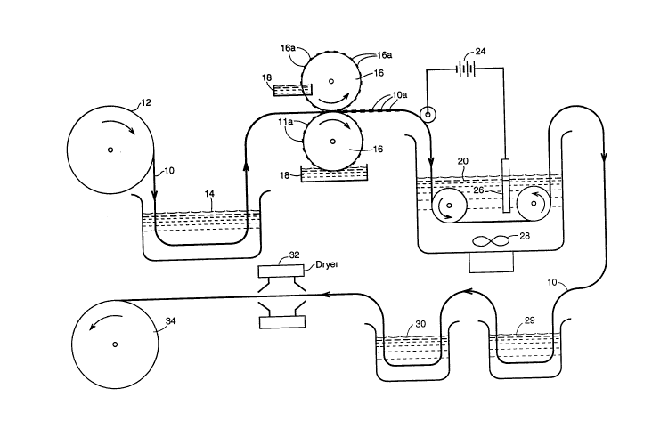
As shown in Fig. 1 a continuou~ thin ribbon or strip 10
of soft magnetic material such as Permalloy or
amorphous metal such as Metglas0, i~ wound off a supply
spool 12. The strip 10 first passes through a
degreasing bath 14 which removes impurities from the
surfaces of the strip. m e degrea~ing bath solution -~ ;
may comprise any conventional commercial
cleaner/degreaser such as methyl alcohol (C~OH).
; ~ ~ ;? ~ ~
~ I ~ 1 i 2 7
The strip 10 then passes between a pair of masking
rollers 16 which have spaced apart mask forming
elements 16a di~tributed along their surface. These
ma~k forming elements pass through a hot wax bath 18 as `
5 the masking rollers turn and in doing so they acquire a ~ ~
coating of hot wax. As the strip 10 passes between the --
rollers 16 it encounters the spaced apart mask forming
elements 16a which deposit spaced apart wax coatings
which form masks lOa on the surfaces of the strip 10. ~ ~
. ., ' '
After receiving the masks lOa, the strip 10 passes
through an electrolytic plating bath 20.
Blectroplating baths suitable for this purpose are
described in U.S. Patents No. 2,834,725 and No.
2,619,454; and they may comprise a mixture of cobaltus
chloride CoCl26~0), nickel chloride (NiCl26~0), boric
acid and pota~sium thiocyanate. Upon entering the bath
20, the film contacts an electrode wheel 22 which is
connected to the negative side of a voltage source 24.
The positive side of the voltage source 24 is connected
to an anode 26, which may be a block or bar of cobalt,
nickel, cobalt-nickel alloy or an insoluble, conductive
material ~uch a~ graphite or platinum immersed in the
plating bath 20. A 8tirrer 28 within the bath 20 keeps
it in constant motion. During its passage through the
bath, the strip 10 has deposited thereon, in the non-
masked region~, spaced apart regions of the high
magnetic coercivity magnetic material, which in this
case is a nickel-cobalt alloy.
After exiting the bath 20, the strip 10, with the
electroplated layer thereon, is passed through a
dewaxing solution 29, which dissolves and removes the
wax masking on the strip. The strip is then directed
into a rinsing solution 30, which may be water, to
rinse off any excess masking material as well as any
excess electroplating solution. The strip then passes
~ ~ 3~ l 27
-- 8
through a dryer 32 which blows hot air on the strip to
dry it. The strip is then wound up on a take up spool
34.
The spool 34 with the electroplated strip 10 wound
thereon i8 then transferred to a cutting station as
illustrated in Fig. 2. Here the strip 10 iq unwound
from the spool 34 and is passed through a pair of
cutting rolls 36 having cutting elements 36a which cut
the strip into individual markers 40. These markers,
which have no covering or other material associated
with them, may then be inserted into articles to be
protected or to packaging for those articles during
their manufacture. This eliminates the need for
attaching the markers to the articles or to their
packaging at the point of retail sale, which is usually
a time consuming and costly operation.
~" " '
The above described process produces what are known as
remotely deactivatable markers. That is, the plated
regions of the markers 40 can be magnetized to
desensitize the markers by application of magnetic
fields from sources which do not touch the marker, 80
long as those fields are oriented along the length of
the marker. The invention can also be used to produce
what are known as colineal markers. In this case, the
step of masking selected portions of the marker prior
to the electroplating step would be eliminated; and the
plating would extend along the entire length of the
marker without interruption.
Two specific examples of the electroplating process
described in general above, will now be described.
. .' .
., .~
.
.
2 ~ ùil~7
g ~: .
. ;
EXAMPLE NO. 1
A plating bath as described in U.S. Patent No.
2,834,725 was used to produce plated film on the strip
10 which was made of known marker material, namely a
ribbon of either Permalloy or an amorphous material
known as Metglas0. Other plating baths may be used,
for example that disclosed in United States Patent No.
2,619,454. Opera~ing parameter~ in this embodiment
were as follows:
Temperature (of the bath): 40-80 Centigrade;
Current Den~ity: 100 amp/ft2 DC and
200 amp/ft2 AC (60 Hz);
(A current density of 200 Amps per foot squared AC
60 Hertz superimposed on 100 Amps per foot ~quared
DC achieves desired semi-hard magnetic
properties.)
pH of the bath: 2.0-3.0;
Time in bath: 2.5 to 10 minutes;
Anode material: Co, Co-Ni, Ni or an insoluble
electrically conductive material such as graphite or
platinum.
~ilm~ of 0.0005-0.001 inch (0.0127-0.0254 mm) were
plated within 5-10 minutes The films 80 deposited were
smooth, bright and adhered to the substrate very well. ~-~
Properties of such as-plated films are given below.
~or comparison, the properties of a ribbon of
Arnokrome~ (a material normally used as a desensitizing
element) are also included.
Sample No. 1 - 2.5" x 0.0625" x 0.0010"
(6.35cm x 2.46mm x 0.025mm)
Sample NO. 2 - 2.5" x 0.0590" x 0.006n
(6.35cm x 2.32mm x 0.015mm)
Sample No. 3 - 2.5 n x 0.0260 n X O . 00101~
(6.35cm x 1.02mm x 0.025mm)
. ~.
. - . - - . . ~ - - . . -., ~ .
. .'"'-,,",'~ f
~ "3 1 1 7
~ , .
- 10 -
Arnokrome - 2 5" x 0.0625l' x 0.0020"
(6.35cm x 2.46mm x0.050mm)
TABLE NO. I
Sample Coercivity Saturation Residual
Induction Induction
(Hc) (B,) (Br)
No. 1 101 311 ~288
No. 2 84 174 158 ;
No. 3 91 100 94
Arnochrome 92 328 300
Note: The values given for saturation induction and
residual induction are given in arbitrary units and are
for comparison only. The coercivity i~ mea~ured in
oersteds.
RXAMPLB NO. 2 ~ ~
` . :.
Markers, i.e. targets, were prepared as described in
~XAMP~ N0. 1, except that the sub~trate or strip 10
was eelectively masked in order to place segments of
the platsd material on the strip. Masking was
accomplished by placing acid re8i8tant tape onto the
8ub8trate at location~ that were to be kept from being
plated, Also, if desired, similar patterns could be
obtained by masking with waxes described in connection
with ~ig. 1 or by coating the strip 10 with wax and
then removing the wax from those areas that are to be ~ x
plated. Alternatively a non-conductive paint or
lacquer can be sprayed onto the strip at locations that
are not to be plated. Photomasking technique~ may also
be used.
~ig. 3 show~, in enlarged perspective view, a marker 40
produced according to the present invention. As can be
seen, the marker 40 comprises a continuous ba~e 40a,
which is the same as the original strip 10, with
.i ~ 7
regions 40b of high coercivity material which has been
plated onto the base 40a. The high coercivity material
has been applied to the base in an atom by atom
deposition process. As a result, an intimate contact
is achieved between the base and the high coercivity
material; and no adhesive or other intervening material
exists between the base and the high coercivity
material. Consequently, the high coercivity material
is effective even in a very thin layer, to bias the
base material into magnetic saturation. It will also
be appreciated that only the precise amount of material
found on the finished target or marker is used in its
manufacture and the cost of producing the marker i9 ` ~-
minimized. Further, this process avoids the need to
separately form high magnetic coercivity elements and
then to physically apply them to the base material.
Because of this, the number of manufacturing steps
needed to make the marker is reduced.
In the embodiment of Fig. 4, the strip 10 i9 not
electroplated but instead the higher coercivity
magnetic material is deposited onto the strip by vacuum
depo~ition.
In Pig. 4 there is provided a vacuum chamber 50 in
which the strip 10 is unwound from a supply spool 52
and is wound back onto a receiving spool 54 within the
chamber 50. Also provided in the chamber 50 is a
crucible 56 which contains a molten alloy 57 of the
material to be deposited, in this case a cobalt/nickel
alloy, preferably about 80~ cobalt and 20~ nickel. The
crucible 56 is provided with a heater 58 to keep the
alloy in a molten state. An evacuation pump 59 on the
chamber 50 operates to maintain a pressure inside the
chamber approximately at 10-3 Torr. (One Torr equals one
millimeter of mercury, or 1/760 atmospheres). The
crucible 56 is maintained at a temperature of about
~' 1 J ` 1 ~ 7
- 12 - - .
: .. .:
1200 C. in order to maintain the alloy in the crucible
in a molten state. The strip 10 is directed to pass
directly over the open top of the crucible 56 as it
moves from the supply spool 52 to the receiving spool
54. The speed of strip movement is preferably
maintained at about 10 cm/min. A faster speed will
re~ult in a thinner deposition and a slower speed will
result in a thicker deposition. It will be appreciated
that the strip 10 may be masked in the manner described
above by means of masking rolls 16 or in any other well
known way to restrict the deposition to non-masked
regions of the strip.
Rig. 5 shows a still further embodiment of the
lS invention wherein the higher magnetic coercivity
material is deposited on the strip 10 by a sputtering
process. In Fig. 5 there is provided a vacuum chamber
60 in which an Argon atmosphere is maintained by means
of a vacuum pump 61 at a pressure of about 1 Torr. The
strip 10 is unwound from a supply spool 62 and is wound
back onto a receiving spool 64 in the chamber 60. A
block 66 of a solid nickel/cobalt alloy (preferably 80~
cobalt and 20~ nickel) is poeitioned within the chamber
60 at a location such that the strip 10 passes over it
25 as the strip move~ from the supply spool to the -~
receiving spool. The block 66 is maintained in a
liquid cooled jacket 68 to keep it from melting during ~ -
the deposition process. An electrode 70, which may be
made of steel, i8 positioned near the surface of the
block 66 which faces the strip 10. A voltage source
72, which is capable of generating approximately 2000
volts, is applied between the block 66 and the
electrode 70. This voltage causes an arc 73 to be
- struck between electrode and the block. This results
in a aputtering action in which a stream of atom~ of
the block material 66a are driven off the block and
thrown against the strip 10. Thus, an atom by atom
" '
, ' ..
~-f J; 1 ~ ~
- 13 -
deposition of the block material is produced on the
strip. Preferably the strip lo is moved between the
spools 62 and 64 at a rate of about lcm per minute.
This ensures that an adequate amount of the high
magnetic coercivity material from the block will be
deposited on the strip. This sputtering action can
take place of room temperature. It will be appreciated
that the strip 10 may be masked in any of the ways
described above in order that the material to be
deposited by sputtering will be applied only to
selected regions of the strip.
It will be appreciated that in each of the embodiments
described herein, a higher coercivity magnetic material
used for desensitizing is applied to the base material
of the target or marker in a deposition process in
which application of the higher coercivity material
occurs on an atom by atom basis. This produces
intimate contact between the base material and the
higher coercivity material; and it avoids the need for
any intermediate adhesive or other material to connect
the two materials. A8 a result, an ef~ective
deactivatable marker can be made with less material and
fewer manufacturing steps than was previously
necessary. Also, the resulting marker is thinner and
more easily handled than prior art deactivatable
markers and is better suited for "source tagging", that
is, application of the marker to goods during their
manufacture.
The process of the present invention may also be used
to produce markers of other configurations, for
example, closed loop markers as shown and de~cribed in
co-pending U.S. patent application No. 08/076,247. In
this process, which is illustrated in Fig. 6, a ribbon
80 of a high magnetic permeability, low coercivity
material such as Permalloy or an amorphous magnetic
, : ,.. - ,: . ,,- ,. . - - -: .. ., . : - ., " , ~ , :, , " -,, : , , .
- .. . , ,. -, .. .. - .. .. , .,,.. ~
2 ~ 2 (
- 14 -
alloy, i~ drawn off from a spool 82. The ribbon 80,
which in the illustrated embodiment is about one inch
(2.54 cm) in width, is first passed through a degreaser
bath 84 which removes impurities from the surface of
the ribbon. The ribbon 80 then passes through a
photoprint machine 86 and an etching bath 88 which
removes material from selected areas of the ribbon
according to a special pattern. This special pattern
is shown in Fig 7.
As shown in Fig. 7, arcuate slits 90 and 92 are etched
out of the ribbon 80. These slit~ form individual
patterns 94 each comprising a pair of concentric
circles. The slits forming each circle are separated
by thin bridges 96 which provide support during
manufacture but can readily be snapped apart at a
subsequent time. Also, elongated arcuate openings 98
are formed by etching in the regions between the inner
and outer circles.
Reverting to Fig. 6, the etched ribbon 80 passes
through a cleaning and rinsing bath 100 and from there
it pa~ses through a photoprint operation 101 which
applies masking in selected regions. This masking is
shown in the dashed outlines 102 of Fig. 8; and ae can
be seen, the masking extends along the arcuate strips
formed on each side of the openings 98. The masking is
resistant to electroplating. The thus patterned and
masked ribbon 80 is then passed through an
electroplating bath 104 similar to that described in
connection with Fig. 1. In the electroplating bath a -
high magnetic coercivity metal, such a~ described in
connection with the preceding embodiment, is applied to
the uDmasked regions of the patterned ribbon.
Following the plating operation, the ribbon 80 i~
passed through a rinsing solution 106 and a dryer 108
.~ ,....
. .
. .
~ 3 ; ~
and is then wound up onto a receiving spool 110. The
ribbon as wound onto the spool 110 appears as shown in
Fig. 9. As can be seen by stippling 112, the entire
ribbon, except for the thin arcuate regions adjacent
the openings 98 is electroplated with the high
coercivity material. Thereafter, when markers are to
be applied to merchandise, they can be snapped out of
the ribbon 80 as shown in Fig. 10. As can be seen, a
ring shaped marker 114 with openingq 98 and thin
arcuate unplated ~trips 116 alongside each opening, is
snapped out of the ribbon 80 and a center circle 118 i9
punched out of the center of the marker.
It will be appreciated that the process of the present ;~
15 invention i8 not limited to the specific shape of the ~`
markers nor to the location on the markers that are
masked; and in fact, for some applications no masking ~
may be used 80 that the entire marker will be plated. ~`
Also, the invention does not depend on the particular `~
type of masking to be used nor on the particular
process used to produce the masking. Further, the
vacuum deposition and the sputtering processes
described above may be used in place of the
electroplating process to produce deactivation elements
on markers of various shapes such as the ring shaped
markers 114 shown in Fig. 10. What is important is
that the deactivation elements be applied on an atom by
atom basis 80 as to achieve an intimate bond between
the marker material and the deactivation element ~`
material.
~`. '
':
':