Note: Descriptions are shown in the official language in which they were submitted.
WO 93/21724 Z1312g5 PCT/CA93/OOlO~
SUBSCRIBER LINE INTERFACE CIRCUIT WITH VOLTAGE CONTROLLED LOOP CURRENT
Technical Field and Tnd~lstri~l Applicability
This invention relates to line in~: r~e circuits for teleco,--",..,-ic~tions lines. Line
intçrf~ce circuits are cbl l 1" ,o~ly cnn--ec~ to two-wire ~lephon~ subscriber lines at a
5 telephone central office or remote t~orrnin~l in order to provide a variety of well-known
desired functions.
Background Art
Various forms of line inlf . r~ e circuit, and various tlf cir~ble fealu,~;s in line
intf rface circuits, are known. In particular, it is known for example from Rose-nb~m
United States Patent No. 4,484,032 issued Nov~ .,.l~, 20, 1984 and entitled "Active
Lll~edallce Transformer Assisted Line Feed Circuit" to provide a line int~f~e circuit in
which two ~n~l.l ;r;. .. ~ have their outputs coupled to the tip and ring wires of a two-wire
lelf~holle line via feed resistors and primary windings of a very small tran~fo~ cl. In this
arr~ng~m~nt, a second~y winding of the ll~U sr~ r and a ,~ ;.isL,vc n ~ ~wOl~ coupled to
15 the feed resistors provide for sensing of a.c. and d.c. conditions on the line.
It is also known from Bolus et al. United States Patent No. 4,431,868 issued
re~l u~y 14, 1984 and entitled "Solid State Telephone Line T~.lf . r~ce Circuit With
Ringing Capability" to provide a line inh~-- r~nc circuit in which a low-level ringing
lefe.~ nce signal can be supplied to the input of high-voltage tip and ring wire amplifiers,
20 to be ~mrlififxl thereby to produce a desired high voltage ringing signal on the line. The
supply voltage rails of the ~.,.,.l;r,...~ are controlled to ~ollow, with an offset, the
ir,~ ,-eous values of the ringing signal waveform in order to reduce power dissipation.
D.c. levels at the amplifier outputs are d~ t.. ;nfA by d c. potlonti~l~ at the amplifier inputs
and the d.c. gain of the amplifiers. This ~rrangçm~nt has the disadvantage that the
25 ~mplifiçr~ must operate with a subs~ gain to pl~luce the large signal amplitudes at
their outputs, and con~e~ently have a relatively narrow bandwidth.
With evolution of telephone systems, it is desir~ble to provide improved line
;lltu. rare circuits which in particular have a bandwidth which is ~urr~ ly great to
acco"",~od~te ISDN (integrated services digital n,twUll~) services, for example a signal
30 bandwidth of the order of 200 kHz. At the same time, it is desirable to provide
improve."cnb in line i~e- r~re circuits with respect to such f~lul~s as their size, cost,
versatility, and operation especially in relation to fault conditions. common mode signal
rejection, and power consumption and ~ ir~tion.
Considered generally, there is a need for a line int~rface circuit which can be used
35 to operate in conjunction with any ~ul il-~uy ~l~,phone col~ nication~ line to provide
~ubiLI~y voice and data co""".l..;~;.l;ons services as may be desired at any particular time
and which the line is capable of carrying, which services can be readily ch~ng~oA under
WO 93/21724 ~95 Pcr/cA93/oolo~
sorlv~al~; control from a telephone central office processor without requiring any hal~lwalc
changes of the line in~prf~e circuit.
While the line int,orf~re circuit desrribecl in United States Patent No. 4,484,032
provides c~ n~ rable advantages over other line interf~e circuits, in particular in
S allowing precise longitll-lin~l balance and the use of a very small ~ rO~ , facilitating
improved noise pelÇollllance and bandwidth which is in~lepc n~ent of the resict~nre values
used in the resistive n~,lwc,lk, which accordingly can be high to minimi7e powerconcumption and ~lis~ t;~n~ n~ ,llllclcss some Ls~lvalllages remain, in particular
relating to noise susceptibility, a residual non-uniÇollllily in the frequency response, and
10 an inability to mol~itor colll,llon mode current s~a,.-t~,ly from dirr~ ial or loop current,
as is deiaud~le in a highly versatile line ;..t~ . r~ce circuit. These disadvantages are
rli~cuc~ further in the det~il~ desc ;I t;nn in this ~ ~;ricdl;on
In order to provide c~ncell~tion of CO.. OI- mode signals, and to provide a
s~bst~nti~lly cons~ll threshold for ground fault current 1imiting, it is known from Rosch
et al. United States Patent No. 4,764,956 issued August 16, 1988 and entitled "Active
Illl~dance Line Feed Circuit" to connect a potential divider ~l~ n the tip and ring wire
voltage taps of the l~,si~ e l~lwulk, in a ~ rO....~ .less line intrrf~r,e circuit, and to
collnecl a d.c. amplifier to the tapping point of the potential divider. The output of th
d.c. ~lnplifilor is coupled to the voltage taps via ùpposit~ly-poled parallel diodes and
20 l~,;.islul~, and the voltage taps are also coupled to a control circuit dirr~ ial amplifier and
to a c~ ~n~ g circuit ~lirr.,l~ ial amplifier. While such an ~rr~n~m~ont provides some
advantages in operation of the line ;I~tl . rh~e circuit, each of the multiple amplifier stages
co~.l- ;h-J~c.s a phase shift, resul*ng in potential in~t~ lity and limited bandwidth. For a
wideb~n-1 line interr~e circuit it is nrxçss ~ y to ...;..;.. ~;'f- dle nUlllte,l of c~ led
25 ~mrlifier stages which are used.
In Rosch et al. United States Patent No. 4,947,427 issued August 7, 1990 and
entided "Protection Arr~ngem~ nt For A Subscriber Line Interface Circuit" there is
~lescri~ an a~ng~m~nt for plv~c~iilg a line interface circuit from faults on the line by
opening conla.;~ of an isolation relay via which the line int~f~re circuit is conll~d to the
30 line. In this arr~ng~ment current on the line is d~tc~ when dhe relay contacts are
closed, by a resistive nelwul~ coupled to the feed resistors, and voltage is detected on the
tclephol1c line side of the relay conl~~, so that the line voltage is ~lr~le(l whether or not
the relay cr nt~-~tc are closed. A c~p~-;lo~ is charged in depPn-l~n(ce upon the ~le~cted line
voltage during positive half-cycles, and in dep~,...1f ~-ce upon the d~ l~ line current
35 eYceeAing a dlreshold level during negative half-cycles, of an a.c. waveform on the line,
and the cAl.Ac;lor voltage is cGnlp~d with a threshold value for controlling the relay.
An object of this invention is to provide an improved line inl~,lr~ce circuit.
Wo 93/2l724 ~ 95 PCT/CA93/0010
Disclosure of the Invention
According to one aspect of this invention there is provided a line intPrf~- e circuit
for a teleco..,..~..n;nations line, co~ isillg: d.c. amplifying means; means for d c.
coupling an output of the amplifying means to a wire of the teleco-...~ -irations line; and
5 means for selectively rl~ ~ . " .;ning a d.c. potential at an input of the amplifying means,
thereby to de~ - . ..;,-e a d.c. level at the output of the amplifying means, comrri~ing a
;~ nr~e and a controlled current source col-lu,~-~d in series ~lv~ en two supply voltage
lines and having a j~ ;O~ e~L~.~n d c. coupled to the input of the amplifying
means, and means for controlling a current passed by the controlled current source to
10 ~ete ~;nr a voltage ~h.,~ed across the resi~t~nre
- Thus the invention enables the d.c. level at the output of a d c. amplifier, and
hence the d.c. po~ ial of a wire of a teleco~ n~irations line which is d.c. coupled
thereto, to be sclecLivGly dc t~ ....;-.ed and controlled in a convenient manner by control of a
current flowing through a lG~ nce
According to another aspect this in~,e.~n provides a line il.tl . r~e circuit for a
two-wire teleco.. -ic-l;o~-~ line, c. mrri~ing: two d.c. amplifiers; d.c. feed means for
courling outputs of the amplifiers to l-,sp~Liv-e wires of ~he line; and means for selectively
~ete. ..,;n;ng d.c. pote..l;~l~ at inputs of the two d.c. amplifiers, thereby to de t~,~ ...;ne d.c.
levels at the outputs of the ~mrlifiPrs, comrri~ing~ for each d c. ~mrlifirr, a ,~sl e~,Live
20 l~ ;.nre and a l~ controlled current source connec~,~1 in series ~l-. ~n two
supply voltage lines and having a junction ~ ~n d.c. coupled to the input of the
I~,s~c~i~e ~mplifirr, and a l~s~lve means for controlling a current passed by the
controlled current source to clet.~ ....;nr. a voltage dlupp~ across the re~i~tAn~e
Thus in acconlal~ce with this aspect of the invention the same p,i"ciple is applied
25 for both wires of a two-wire line, so that the d.c. potential on each wire can be
in~l.,~ n~ nlly controlled. With d.c. ~mrlifi~r~ each having a gain of applo~; . "~ y unity,
and with a~lu~,liat~, se1e~l;oll of re~i~tAnce and current values, the d.c. pol~nlial on each
wire can be varied to be a ,~wl-~, e in the range defined by the supply voltages, for
,lc in the range from 0 to ~8 volts. This provides con~i~erable advantages in that
30 the voltages on the wires can, for example, be l~;~,el~ed for ~ignAlling purposes without
~uiling use of a relay, be varied to reduce cu"~.,~ during fault conditions, and be
adaptively adjusted to provide reduced loop ~;UII~;IIt~ for short lines of relatively low
resictAn~e or to ~-cc..----.~1~te other desired Op~ lii1g con~itions
In order to farilh~t~ digital control and pro~;1.-----Ability, each ,7~;.~ili~/e means for
35 controlling a current passed by the controlled current source advantageously compri~es a
e digital-to-analog cc".~e. ~. for supplying an analog signal for controlling the
controlled current source in depen~ence upon a respective digital signal supplied thereto.
~ ~312~5
As such control is effected in discrete steps whose size is dependent upon the
resolution of the digital signals, the circuit preferably includes means for smoothing the
d.c. potentials at the inputs of the d.c. amplifiers. This means is conveniently con~tihlted
by coupling capacitors which serve for coupling an a.c. signal with opposite phases to the
5 inputs of the two d.c. amplifiers for tr~nsmis~ion on the line.
In order to enable rapid d.c. potential changes when required, without the
smoothing effect of the coupling capacitors, the circuit desirably includes means for
selectively discharging each of the two coupling capacitors. Such means can comprise
two switched current sources, each connected in parallel with a respective resistance, and
10 means for controlling each of the switched current sources.
The line interface circuit desirably includes means, coupled to the d.c. feed means,
for monitoring ~ e~ , on the two wires, the means for selectively determining d.c.
potentials at inputs of the two d.c. amplifiers being responsive to the monitored currents.
The means for monitoring currents preferably comprises means for monitoring loop15 current and common mode current on the two wires of the line, thereby enabling the
individual current on each wire to be readily determine~l Conveniently the means for
selectively determining d.c. potentials at inputs of the two d.c. amplifiers comprises
digital control means and the means for monitoring currents comprises means, such as an
analog-to-digital converter, for supplying digital signals representing the monitored
20 ~ lell~s to the digital control means.
Brief Description of the Drawin~s
The invention will be fur~her understood from the following description with
reference to the accompanying drawings, in which:
Fig. 1 is a block diagram illustrating components of a programmable telephone
25 line interface circuit; and
Figs. 2 and 3 are circuit diagrams illustrating parts of the line interface circuit of
Fig. 1.
WO 93~21724 ~95 PCT/CA93/0010
Mode(s) of Carrying Out the Invenetion
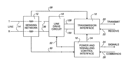
Referring to Fig. 1, there is illustrated a block diagram showing main cû~l~p.ollel~ts
of a pro~al,l,l.able telephone iine inl. . ri~e circuit, which is ~ -.~ in the following
description to form part of and be located at a te~ honF central office (not shown), or CO,
S but which may qlt~rnqtively form part of a remote t~rminq-l which is coupled to a CO via a
mllltirl~l~, cGllllllllll;~ ns path.
These main co,l,~ollenls of the line interface circuit co.~l.. ;ce a line drive circuit
10, a sensing network 12 via which the line drive circuit 10 is coupled to the tip wire T
and the ring wire R of a telephone line 14, a tr~qncmiccion ;nh - r~ce 16 which
0 cG~ n;c~es with the remqin~lpr of the CO via l.~n~..;l and rece*e signal paths 20 and
22 l~,~cc~i~ely, and a power and ~i~qlling control ;n~.. ri-~e 18 which cf~ içq-tçs
signals to and lcce;~,es pro~,.. ;,-g cfJ.. ~n(ls from other parts of the CO via lc.. ~c~ e
paths 24 and 26 l~,~.~,.ec~i~,ely. As further ~es~ibe~l below, the sensing network 12
supplies sensed current and voltage signals to the;nt~,. r"ccs 16 and 18 via paths 28 and 30
15 l~ ,ly, and the int~ . ri~ce 18 su~p.L;~s control and other signals to the line drive circuit
10 and to the trnsmicciQn int~rfqce 16 via paths 32 and 34 r~ ;~ively. In the drawings,
including Fig. 1, where desirable for ~inlrlicity and clarity multiple line paths are
Jl.,senlcd by a single line with a transverse bar.
The line i~h~.. ri ce circuit of Fig. 1 is ;.lt~ n~l~A to be operable, with a~lu~ ate
20 co------Ands, ;"~ down-loaded P1U~IAnllll;ng surlwalc, sul)pl;ed to the ;ntu~ r~e 18
from the CO and used for control pul~oses and for setting up the tr~ncmiccion ;..~,. r.-~e
16 in a desired manner, to provide any of a wide range of co....~ ;cations services for
any of a wide range of co~ n;~al;- nc e~ui~ nl (not shown) coupled to the telephone
line 14. Accordingly, this single form of the line interfi~l~e circuit can be used for
25 extensive types of services without any l-~dwa~, ch~ngçs, simply by appl~liale
sorlwdl~, control from the CO. This results in sul,~ l collllll~,lcial ~.-el ilc, in that only
a single design of line int~f~ce circuit need be n.,.. r~ 1 and inct~lle~ to provide
~I,illaly c~ .;c~tionc services, and the line ;n~ - rA~-e circuit can be easily reconfigured
under suflw~; control to change the services which it provides.
Examples of co.-----~ ti~nc services which can be provided by the single design
of line int~f~ce circuit include reci~lenti~l telephf l-~ services such as Cu~lO~CI local area
cign~lling (CLASS) and call management (CMS) services, multi-party services, andfrequency selective ringing; business tcl~hont and data services such as individual line,
~tten~l~nt console, mes~C~ge waiting, coin, ISDN U, and switched voice~ncl data services;
and switched special services such as Centrex lines, WATS lines, and direct ~ lling
In order to provide such services, the line ;lltf . I~re circuit provides a large l~ulllber
of ~aIU1~S through the design and arr~n~m~-nt of the il~.c. r; ~es 16 and 18, including
ringing, dial pulse digit collection, loop or ground start, DC feed with current limiting,
WO 93/21724 ,~ PCT/CA93/0010
low power standby, battery reversal, modem tr~ncmiscion~ ABCD bit cign~lling, CLASS
and DTMF tone tr~ncmiccion, on-hook and off-hook sign~lling, and surge protection
with aulo-natic recovery. To this end, the tr~ncmiccion intfrf~ce 16 comprices a digital
signal processor and codec (coder-decoder), control soflw~; for which is supplied from
S the CO via the i~lf . r~e 18 and the paths 34. The interface 18 comrri~es a processor,
memory, co., ...~....;r~tions ;.-~ . r~ces, and control circuits for controlling the overall
functioning of the line inte~rface circuit. Except for parts described below with lc;re~ ce to
Fig. 3 of the drawings, these intf rfaçes 16 and 18 are not described further here.
Fig. 2 is a circuit diagram illustrating parts of the sensing network 12, and Fig. 3
10 is a circuit diagram illus~ g the line drive circuit 10 and associat~;l parts of the
i~t~ r~ces 16 and 18. Output lines 36 of the line drive circuit 10, shown at the left-hand
side of Fig. 3 and also i~-d;c~tf~ in Fig. 1, are coupled to the tip and ring wires of the
telephone line 14 via the sensing n~,lwo,~ 12 as already e~pl~inf~ above.
Referring to Fig. 2, the wires 36 are couplf~ to the telf phone line tip and ring
15 wires T and R via primary win-ling~, ~nsed as shown by dots ~ Cf nt the win-lings, of a
transformer 38, .~ f~l feed resistors 40, and relay cor~t~tc 42. A resistor network 44
is co~ f~1 to the feed l~ ol~ 40 to provide on lines 46 a ~l~nce~l output dependent
upon current flowing through the feed ~i,is~,~ 40 and on the telephone line 14. A
sfxo.~d~.y winding of the tran:,Ço,.--el 38 provides on lines 48 an outputdfpenrlent upon
20 the dirrel~lia~ h ~- ~ g current flowing through the primary windings and hence on the
telephone line 14.
The two lines 46 are co~ln~t ~1 to the inverting inputs of ~e~ e differential
arnplifiers 50, whose non-inverting inputs are supplied with a reference potential Vr. For
conveni~n-~e, the label Vr is used co....nollly at various places in Figs. 2 and 3 to denote a
25 reference potential, for exarnple half the supply voltage, but it should be understood that
dirr~ actual values of reference l,ot.,..~al can be provided at dirr,lell~ ones of these
places to provide desired op~ g conditions. The output of one of the arnplifiers 50 as
shown (or ~lt~orn~tively the dirrel~l~tial outputs of the two arnplifiers 50) con~ es a
signal ID on the line 28. This signal ID l~ ,se.lb the ~lirr,l~ ial current on the telephone
line 14, and is supplied to the tran~mi~ion i.~ . r~re 16 as already describe(l
Each of the arnplifiers 50 has a d.c. feedbflc~ path from its output to its inverting
input via two series-connected resistors 52 and 54, and an a.c. feedb~c~ path from its
output to its inverting input via a series-connected resistor 56 and c~c; lor 58 connected
to the junction between the ~Si~lu~S 52 and 54. Each line 48 from the secondary winding
of the tran~ro~ , 38 is conn~ ~1 to a re;,l,e ;li~/e junction ~Iwee-l the resistor 56 and
capacilor 58.
A potential divider is formed by two resistors 60 com~ ed in series bet-ween theoutputs of the ~mplifi~rs 50, the junction l;~ ,ell these resistors being connecte~l to the
wo 93/2l724 ~; pcT/cAs3/oolo~
non-inverting input of an amplifler 62 whose inverting input is supplied with a reference
potential Vr. The output of the amplifier 62 is coupled via lc~Li~e resistors 64 to the
two lines 46.
Another potential divider is formed by two resistors 66 connecLed in series
5 be~ the tip and ring wires T and R of the lelepholle line 14, on the line side of the
relay CGIl~ClS 42. The junction b~ ,.~n these resistors 66 is co.~ lc~ to a ~ g
node 68, to which the output of the amplifier 62 is coml~;Lcd via a resistor 70. The
~I~n~ g node 68 is COI-~ t~ to the input of a buffer amplifier 72, whose output can
col~ a COIlllllOll mode voltage signal VCM on a line 74 which con~lilu~es one of the
10 paths 30 in Fig. 1.
The line 74 is also COI~l~f,Cl~d via a resistor 76 to the inverting input of a dirr~.cll~ial
~mrlifiPr 78, whose non-inverting input is supplied with a ~if~.~nce potential Vr and
whose output, which is C-~nl~f.~ via a Çc~lbA~L resistor 80 to the in~,e. Ling input, is a
collllllon mode current signal ICM on a line 82 con~ ulillg another of the paths 30.
15 further one of the paths 30 is conctitlltp~l by a line 84 carrying a loop current signal IL
from the output of a buffer ~mrlifiçr 86. The input of the buffer amplifier 86 is connected
via a resistor 88 to the line 28 and via a c~;lor 90 to 3round, the resistor 88 and
capaciLor 90 together forming a low pass filter with a corner fre~uency of about 200 Hz.
The ~rr~ngPrnPnt of the ~ul~Çullll~,l 38, feed resistors 40, and resistor network 44
20 as ~les~r~ above and ill..cl.,.t~1 in Fig. 2 is known for e~ le from United States
Patent No. 4,484,032 already l~f~ d to. This arrangement allows precise longitu-lin~l
balance of the circuit to be achieved, using a very small l,ansrollll~,. as the transformer 38
for a.c. sencing, and using resistors ,..~t~ 1 to or~lin~ y tolerances (for example 1%) for
the feed resistors 40 and resistor nclwolk 44. High recict~nre values used in the resistor
2~ network 44 reduce power consumption during idle conditions (on-hook state of a
~lephol~ co~-necl~l to the line 14), and the tran~rullll~,. facilit~tes good noise performance
and a bandwidth independent of the resistor values used.
As described and illusll~ in Patent No. 4,484,032, one t~o.rmin~l of the
secondary winding of the transformer is ~uunded, and the other terminal is capacitively
30 coupled to the inverting input of a dirr~ ial ~mplifi~r having a.c. and d.c. fee~ba~k
paths. The non-inverting input of the dirr~ ial amplifier forms a ground l~fi,.~nce for
the ~...plir;~ " whose gain is d~,t~.lllih~ed by the ratio of an a.c. Çee~db~cL resict~n~e (96 in
Fig. 3 of the patent) to the reci~t~nce of the secon-l~ry winding of the transformer. As the
latter is desirably small, this gain is relatively large. Any potmti~l dirr~ ,nce between the
35 grounded t~m~in~l of the transformer secon-l~ry winding and the ground lefc.~,nce at the
non-in~,~.Ling input of tAhe amplifier con~ti~ltes a noise source, which is amplified by this
large gain. F.~peri~lly where the ~ r~ is imple...~ I~t~1 in an inle~aled circuit, as is
Wo 93/21724 ~ PCT/CA93/0010
dPcir~hle for economy and small size, such a potential ~liffi,lcnce and concequ~Pnt noise is
difficult to avoid.
This disadvantage is avoided by the use in the circuit of Fig. 2 of the two
amplifiers 50 in a bAlAnce~l configuration. The amplifiers 50 operate with opposite phase
S sy~ . ;cally about the l-,f,lc--ce pot~,nlial Vr supplied to their non-inverting inputs,
which det~ u~e s the potential of the lines 46, so that ~usceplibility to diffel ,nlial ground
noise as in the prior art is çl;...;n~
This an~n~ment has the advantage, co--.l)a cd with the multi-stage coccade~
amplifiers of United States Patent No. 4,764,956 already rcfcll~,d to, that only a single
10 stage of ~rnrlifi~otion (split bcl~n the two bro1Ance~ ~mrlifiPrs 50) is used to provide a
diff~ ,nlial mode output signal, and no compensation scheme is n~cesc~ly as in that patent
b~cause of the b~1Oncecl or s~/.. e~ A1 &l~ngen.~ of the An~l l;r.l .~ 50. This
arrangement thus provides less phase shift, and hence more stable operation over a greater
bandwidth, than this prior art.
As in the prior art r~,pn,sent~l in Fig. 3 of United States Patent No. 4,484,032,
the a.c. and d.c. fee~hAck paths of the sensing Arnr1ifiçrs 50 are ~n~ng~3 to provide the
same gain for a.c. signals as at d.c. In the prior art, the secondary winding of the
tran~rolll.e,l is coupled to the inverting input of the sensing ~nlrlifiPr via only a coupling
c~ o~ ol which forms part of the a.c. fee~lboc~ path of the ~ )1;r.r ~. However, because
20 the ~ rOl,,l secolld~y winding has a finite resir~tonre~ there is a voltage drop across
the coupling capa~ or which in turn causes a variation jn gain and phase in the transition
bet~een d.c. and a.c. signals. This can give rise to distortion of low frequency a.c. or
pulsed d c. signals, such as dial pulses, or to in~tAbi1ity when the output of the amplifier
is used in a feedback loop for d.c. control purposes.
This problem of the prior art is avoided in the circuit arr~ngçmPnt of Fig. 2 by the
provision of the resistors 54, one for each of the amplifiers 50 in view of the bo1Ance~l
arrongemPnt To ~-,.~le.~ l this, it can be seen that the outputs of the A~ irif.. j 50
swing in a holonreA manner and with ol~posile phase about the l~,f~ ,l.ce pc~l.tial Vr
applied to the non-inverting inputs, so that the mid-point of the l-~ulsrwl--er secontlory
30 winding is at this reference potential and hence at the same potential as the lines 46. For
each side of the bA1~nce~1 arr~n~m~nt, the coupling ca~ ilo 58 is connP~-I~A belweell the
tapping points of two potential dividers b~ ~n the output of the ~plifiP,r 50 and the
crcl~,llce potential Vr, one formed by half the ~es;~ c of the seconda- ~ winding in
series with the resistor 56, and the other forrned by the resistors 54 and 52. By making
35 the ratio of these two l)o~nlial dividers equal, there is no net voltage across the capacitor
58, res111ting in a more uniro~ mr1ifier lc~onse in the transition from d c. to a.c.
signals.
wo 93/21724 ;~? ~ i PCT/CA93/OOlOS
In other words, e"l,le.,sing the resi~t~nres of the resistors 52, 54, and 56 and the
tran~,Çoll"cl secondary winding as R52, R54, R56, and Rw l~,~e~ ely, the resi~t~nce
values are selected so that R54 = Rw x R52 / 2 x R56. However, it should also beappreciated that this relationship may be m~ified if desired to control the transition of the
S arnplifier response be~ ,ell d.c. and a.c. signals, for e~".ple by over-co"~pens~ting for
the tran~,rull"~,l winding re~i~t~n-e to provide, with a desired caraci~nce of the c~pacitor
58, an ~ l;on at a rl~u~ ;y of 60 Hz.
The ~mrlifi~. 62 serves to reduce co,ll,llon mode signals on the lines 46, through
the coupling of its output to these lines via the resistors 64, in a similar manner to that of
10 the prior art except that, in view of the b~l~n~efl arr~n~om~nt of the circuit, the non-
in~ ling input of the arnplifier 62 is c- nl~F~t~l to the tapping point of the potential divider
formed by the resistors 60 co,.n~t~d ~l~.~n the outputs of the ~mplifi~rs 50, and the
inverting input of the ~mplifier 62 is conl-~t~ to a l~,fel~llce potential Vr.
In order to d~,h ., l~h~c all of the ~;ullcrib on the ~ l~ phone line 14, it is ,-ece~ y to
15 lnonilur the c~,....,OI~ mode current on the t~,lepholle line as well as the dirr~ llial current,
ep~ t~d by the signal ID, or the loop current"~ ,se.it~ by the signal IL. The loop
current signal IL is produced on the line 84 from the ~lirr.,l~ ial current signal ID by
filt~ring in the low-pass filter con~l;l.,t~ by the resistor 88 and ca~ or 90 and burr~,li"g
in the buffer ~mrlifiPr 86. The low-pass filt~ring ~ t,us frequency co...l~ol-~ above
20 about 200 Hz, so that the signal IL l~ SCn~7 the d c. loop current. The ~;u~l~nls on the
tip and ring wires of the telephone line are l~,*,f~;lively the sum and dirr~,lence of the
CO....,,OI- mode current and the loop current.
The output voltage of the ~mrlifi~r 62 is (-VT - VR + Icm x R40) x R64 / R44,
where VT and VR are the voltages of l~,~;lively the tip and ring wires T and R of the
I~,k~)holle line 14, Icm is the ch~"~on mode current through the feed ~esi~ 40, R40
and R64 are the reSi~t~nces of each of the resistors 40 and 64 l~ ively, and R44 is the
resi~t~nce of each of the ~ in the resistor nclwfJIL 44. At the s~ -...n;..g node 68,
this output voltage is s~l"""fA with a voltage derived from the potential divider formed by
the resistors 66 and which is ~le~ cnl upon the colll,lloll mode voltage and not on the
colll,llon mode current. This voltage is given by (VT + VR) x R70 / R66, where R70 and
R66 are the resi~t~nces of the resistor 70 and each resi~t~n~e 66, l~ f~lively. The
resi~t~nre values are self~te~i so that R66 / R70 = R44 / R64, wh~,le~y at the 5u~ 1 ,l, l;l lg
node 68 the ~..."...~ voltage is in~lepun~lf nl of the colll~llon mode voltage colll~onelll
VT + VR, and ~ scllts only the CO.. OI- mode current. This s.. ~1 voltage at the
node 68 is burr~ d by the buffer ~mplifi~r 72 and ~nlrlifiç~ by the amplifier 78, whose
gain is ~ " ~; n~l by the resistors 76 and 80, to provide the signal ICM on the line 82
~,~.ll;ng, with a desired sensitivity, the colllllloll mode current on the line 14.
~ ~ 3 ~ 29~
When the relay contacts 42 are opened for example for protection of the line
interface circuit, the common mode current through the feed resistors 40 becomes zero.
The output voltage of the amplifier 62 then represents only the sum of the drive voltage
levels provided by the line drive circuit 10 as described further below, while the common
mode voltage on the telephone line 14 continues to be monitored via the resistors 66.
Accordingly, the su~ llhlg node 68 in this situation is at a summed voltage representing
the common mode voltage on the line 14 referenced to the sum of the drive voltage levels.
This summed voltage, buffered by the buffer amplifier 72, constitutes the common mode
voltage signal VCM on the line 74. Thus common mode voltages on the line 14 are
monitored when the relay contacts 42 are open.
Referring now to Fig. 3, there is illustrated a circuit diagram of the line drive
circuit 10 together with a signal coupling circuit 100, which can be considered to form
part of the tr~nsmi~ion interface 16 in Fig. 1, and control circuitry 102, which can be
considered to be part of the power and signalling control interface 18 in Fig. 1.
The signal coupling circuit 100 comprises two differential amplifiers 104 and 106,
resistors evenly numbered from 108 to 116, an impedance (Z) 118, and a capacitor 120.
The impedance 118 can comprise fixed or switched reactive components as is known in
the prior art, but for full versatility of the line interface circuit is preferably a
pro~l,lllable impedance.
The differential current signal ID on the line 28, coupled via the capacitor 120,
constitutes a transmit path signal Tx and is also fed back to the inverting input of the
amplifier 104 via the impedance 118 and the resistor 110. A receive path signal Rx is
coupled to the inverting input of the amplifier 104 via the resistor 112. The amplifier 104
has its non-inverting input coupled to a reference potential Vr, and has a feedback path
including the resistor 108 from its output to its inverting input. The resistor 108
determines, with the resistors 112 and 110, the gain of the amplifier 104 respectively for
the receive path signal Rx and for the signal fed back via the impedance 118.
The output of the amplifier 104 is supplied on a line 128 to the line drive circuit
10. The resistors 114 and 116 and the amplifier 106 together form a unity gain inverter
which inverts this output and produces a complementary output on a line 130 to the line
drive circuit. The lines 128 and 130 are also referenced in Fig. 1.
The d.c. blocking of the signal rD by the capacitor 120 results in the impedance118 and the amplifiers 104 and 106 having to accommodate only the relatively low voltage
signals being tr~nsmitt~(1 and received, and not larger d.c. components which may exist
on the telephone line 14. Consequently, the amplifiers 104 and 106 can be designed to
WO 93/21724 13129S PCT/CA93/0010
~ t~,
11
have a large bandwidth as is desired, with the Amplifier 104 still providing a ~ignificAnt
gain.
The line drive circuit 10 comprises two d.c. buffer amplifiers 132 and 134 whoseoutputs are conn~-~ to the wires 36 on l~,s~;li./ely tip wire and ring wire sides of the
S line drive circuit. The outputs of the Amplifiers 132 and 134 are also col-l-e~-~d directly to
the inverting inputs of the Amplifi~rs, l~,~e~ ely, to provide unity gain so that these
~mrlifiers have a .~.~xi.. n~ bandwidth and a .. ;n;.. ~ " output ;.. ,l~A.,ce The line 128 is
a.c. coupled to the non~ c~ g input of the ~mrlifi~r 132 via a capacitor 136, and the
line 130 is a.c. coupled to the non-inverting input of the Amrlifi.or 134 via a cApacitor 138.
It is observed that the amplifiers 132 and 134 need not l-P~es~A~ily have a gain of
exactly unity as desçribe~l here and as illustrated in Fig. 3. They may AlternAtively provide
a desired gain, providing a plu~llional relationship between the d.c. potentials at their
inputs and outputs. However, as any such gain decreases the bandwidth and increases
the output ;. . .l~lAn~e of the Arnplifiçrs, it is ~ie~ir~hly kept small and apyro~; . "A Irs to a
lS gain of unity.
The non-inverting input of the ~ ~pl;rlel 132 is a!.so coupled via a resistor 140 to a
supply voltage +V, and via a controlled current source 142 to a supply voltage -V. It is
also coupled to the supply voltage +V via a ~wilched current source 144, in parallel with
the ~ lur 140. Conversely, the non-inverting input of the amplifier 134 is also coupled
via a resistor 146 to the supply voltage -V, and via a controlled current source 148 to the
supply voltage +V. It is also coupled to the supply voltage -V via a ~wilched current
source lS0, in parallel with the resistor 146. The supply voltages +V and -V mayconveniently be the CO battery voltages of ground and -48 volts ~ ely, and this is
u~,.~ in the following d~s~ ,lion, but other voltages may be used if desired.
Currents passed by the current sources 142, 144, 148, and lS0 are controlled by a
digital control circuit 152 which forms part of the control cil.;uiLIy 102. The switched
current sources 144 and lS0 are controlled via lines 154 and 156 l~,ecli~ely simply to be
on or off as further described below; these sources can ~A~lt~rnAtively be replaced by
~wilclled l~ lul~. The controlled current sources 142 and 148 are precisely controlled
by eight-bit digital signals supplied by the digital control circuit 152 to digital-to-analog
converters 158 and 160 l~pe~ ely, and thence by stepped analog signals on lines 162
and 164 ,~,~ecli~ely. The lines 154, 156, 162, and 164 constitute the paths 34 in Fig. 1.
The signals IL, ICM, and VCM on the paths 30 are supplied to inputs of a
multiplexed analog-to-digital con~,eltel 166, whose digital outputs are supplied to the
digital control circuit 152. The digital control circuit is also supplied, as already expl~in.o(l
with ,~,f~,nce to Fig. 1, with co,- In~An~l~; in acco,dal~ce with which it ~lc t~ ,ines
ap~,u~liate o~l~ling conditions for the remAin~ler of the line i"~ . r~re circuit and provides
control signals acc~"~lingly. As part of this control, the di~ital control circuit 152, which
WO93/21724 ~ J ~.. pcr/cA93/oo1o5
Z:13129~ 12
for example is con~ 1 by a digital state m~rhine"noni~l~ the .1igiti7~l signals IL,
ICM, and VCM to detect (possibly faulty or undesired) op~ ling cc.n-lhions some of
which are discussed further below, and inctig~tec action to adapt the line interface circuit
in relation to such conditions. This action may in particular include control of the current
S sources as desçribe(l below, and control of the relay contacts 42 for protection of the line
int~rf~r,e circuit.
By way of eY~mpl~, it is observed that the resistors 140 and 146 rnay have
resict~nres of about 320 kQ, the swilched current sources 144 and 150 may pass a current
of either 0 or 10 mA, the controlled current sources 142 and 148 may pass a precisely
controlled current in a range from 0 to 150 ~A, and the cap~ci~l~ 136 and 138 may have
c~p~rit~nces of about 0.22 luF.
I~ecause the capacilor 136 blocks d c., the d.c. voltage level at the non-inverting
input of the ~mplifi~r 132 is d~t~,.lllined by the supply voltages +V and -V, the resict~nre
of the resistor 140, and the controlled c~ passed by the current sources 142 and 144.
15 Simil~rly, the d c. voltage level at the non-i~ .Lillg input of the amplifier 134 is
d~ h ..~ A by the supply voltages +V and -V~ the le~;c~ e of the resistor 146~ and the
controlled ~;ull~nls passed by the current sources 148 and 150. The ~mrlifiers 132 and
134 are d.c. ~mrlifi~rc having a desired large bandwidth, unity gain as described above,
and a large d.c. voltage range, so that the d.c. voltage levels at their non-i"~ ng inputs
det~.. ne the d.c. voltage levels at their outputs and on the wires 36, and hence on the tip
and ring wires T and R of the tel~hol-e line 14.
Con~ ring the tip side of the line drive circuit, the current source 144 is normally
off so that it passes no current. The controlled current source 142 is controlled, for
çY~mple in 256 discrete steps d~ -~1 by the 8-bit output from the digital control circuit
152 to the digital-to-analog col,~,.t~,. 158, to pass any desired current in the range from 0
to 150 ~A. This current flows through the resistor 140, which accol.lingly drops a
voltage ~lepen~l~nt upon the current and which can be from ~ro to the dirr~ "ce between
the supply voltages +V and -V. Accordingly, the control of the controlled current source
142 enables the d.c. voltage at the non-inverting input of the ~rnrlifi~ 132, and hence on
the tip wire T, to be steered to any desired level from +V to -V. With the resistor 140
having a reci~n~e of 320 kQ and the supply voltages +V and -V being ground (0 volts)
and ~8 volts as intli~t~ above, the tip wire T can be set to any desired voltage from 0 to
~8 volts.
Simil~rly, on the ring side of the line drive circuit the current source 150 normally
passes no current, and the controlled current source 148 can be controlled via the
converter 160 to pass any current from 0 to 150 ~A to drop a voltage from 0 to 48 volts
across the resistor 146, so that the non-inverting input of the amplifier 134, and hence the
ring wire R, can be steered to any voltage from J,8 to 0 volts. It should be noted that the
WO 93/21724 Z131295 PCT/CA93/00105
settings of the d.c. voltage level of the tip and ring wires T and R are independent of one
another, so that each wire can be set to any voltage in the desired range ~lween the
supply voltages +V and -V. It should also be noted that the connections of the resistors
140 and 146 to the supply voltages +V and -V respectively enables the most coll""on
S situation, of these voltages being applied to the tip and ring wires l~,~ccli~ely, to be
provided with the ~.. in;.. power co~.~----.lJtion.
~ The current sources have a high ;~ n~-e so that they do not adversely affect
the capacili~e coupling of a.c. signals from the outputs of the ~mrlifitors 104 and 106 to
the amplifiers 132 and 134 le*,e;~ ely. The ~mplifi~rs 104 and 106 have low output
i~ )~An~es~ so that the resistor 140 and c~cilc)r 136, and likewise the resistor 146 and
C~p~C;IOl 138, form low pass filters each with a pole at a sufficiently low frequency, for
çYAmple about 3.5 Hz, to filter out any residual a.c. noise on the d.c. control signal lines
162 and 164. This low pass filtering action is also of particular benefit in the normal
course of operation in ch~nging the d.c. voltage levels, because it smooths or filters out
15 the discl~,t~ steps as the d.c. voltage level is çhAnged so that there is no deE~adalion of
trAn~mi~sion p~ru.l-.An~e.
As a result of the filt~ring action, when the current passed by the controlled current
source 142 is l~ ce~l the tip voltage set at the non-inverting input of the amplifier 132
will become more positive at a relatively slow rate d~,t~ by the tirne COI~ t (about
20 70 ms) of the resistor 140 and the c~ J. 136. While such a slow rate of change is
desirable for some op~ ing ~itll~tion~ of the line int~rf~re circuit, a fasterrate of change
is desirable in other situations. Where a fast rate of change is desired, the swi~ched
current source 144 is turned on, under the control of the digitA~ control circuit 152 via the
line 154, for a short period d~,t ....;..ed by the digital control circuit, to discharge the
ci~pacilor 136 at the higher current, for c.~.. ple 10 mA, passed by the current source 144.
SimilArly, the ~wilched current source 150 is turned on by the digital control circuit 152
via the line 156 to make the ring voltage level more negative at a faster rate than is
p~ ....;11~ bythetimecon~t~ntoftheresistor 146andcapa~ ol 138.
The in~lep~n(l~ nt control of the d.c. voltage levels on the tip and ring wires as
30 described above is useful for a variety of purposes, during normal operation, for
protection against faults, and for self-testing of the line int~rf~G circuit. For example, in
normal operation this indGy~,ndent control enables battery reversal conditions, for example
for sign~lling purposes, to be set up without using a relay. In addition, the d.c. voltage
applied to the telephone line can be set in dep~ lf nce upon the loop current signal L
35 supplied to the digital control circuit 152 in order to lirnit the loop current to a desirable
low level, wl~ by power cu,,su,,,y~ion is reduced and the line int~rf~ce circuit is
adaptively adjusted for different loop ~ nces. For protection purposes, for example in
WO 93/21724 2131295 PCTtCA93/0010~ -
14
the case of a ground fault (ring wire shorted to ground) the voltage level of the ring wire
can be ch~nged towards 0 volts to limit current during the fault.
It should be appreciated in this respect that the provision of both the loop current
signal IL and the col.lmon mode current signal ICM to the digital control circuit 152
S enables this circuit to de~ e both the tip wire current (co....-.ol- mode current + loop
current) and the ring wire current (c~ nl~ mode current - loop current), so that the d c.
voltage levels supplied to the tip and ring wires can be individually d~,t~ ed in relation
to the tip and ring wire ~;u~ s.
Although a particular e .~l~l;...~-nl of the invention has been described in detail, it
10 should be appreciated that nUlll~,~uus mo 1ific~tionc, variations, and ~ n~ may be
made.