Note: Descriptions are shown in the official language in which they were submitted.
2,~3:t339
- 1 -
TITLE OF THE INVENTION
Electronic power converter circuit arrangement and
method for driv:tng same
BAOItGROUND OF THE INVENTION
Field of the Invention
The invention relates to the field of power
electronics.
It proceeds from a method for driving an '
electronic power converter circuit arrangement
according to the preamble of the first claim. It
relates, furthermore, to an electronic power converter
circuit arrangement.
Discussion of Background
Such a method and an electronic power converter
circuit arrangement have already been described, for
example, in the article by A. Stamberger "Serie- oder
parallelgeschaltete Hochleistungs- GTOs mit genau
synchronisierter Abschaltung", ("Series- or parallel-
connected high-power GTOs having a precisely
synchronized turn off"), Elektroniker No. 3/1985, pages
68-72.
If the individual arms, for example, of a half-
bridge contain series-connected power semiconductor
switches (GTOs in the abovementioned article), this can
lead to a bad, that is to say irregular voltage
distribution. This can lead further to overloading of
individual semiconductors of the series circuit. The
reasons for this unequal loading reside in different
turn-off times, differences in the parameters of the
semiconductors and of the associated circuits, as well
as parameter changes during operation.
In the abovementioned article, an attempt is
made to balance the voltage loading of the individual
switches by controlling the turn-off times of the
control signals in sudh a way that all the GTOs of an
electronic power converter arm start to block
simultaneously. The instant of the turn-off signal is
used as controlled variable.
~13~339
-'2 -
However, only the turn-off time is exactly
corrected thereby. Irregular voltage loadings due to
parameter differences and parameter changes cannot he
balanced, however, since it is not possible to provide
any information on the exact voltage distribution.
Moreover, the method previously explained acts only
during switching, more precisely during turn-off.
Differences in voltage loadings in the steady state of
"blocking" still remain out of consideration, although '
these could occur because of parameter differences and
parameter drift.
Consequently, the correction is incomplete and
the utilization of the semiconductors is not optimal.
In the case of applications in relatively large
semiconductor modules (0.5 MVA switching capacity and
more), this can have unfavorable effects.
SUl~giARY OF THE INVENTION
Accordingly, one object of this invention is to
provide a novel method for driving an electronic power
converter circuit arrangement, and to provide an
electronic power converter circuit arrangement in which
the abovementioned disadvantages of the prior art are
to be avoided. In particular, the control of the
voltage distribution is also to take account of
parameter differences and changes and is to come into
play in the steady state.
This object is achieved in a method of the type
mentioned at the beginning by means of the features of
the first claim, and in a circuit arrangement of the .
type mentioned at the beginning by means of the
features of the seventh claim.
The core of the method according to the
invention is, thus, that the voltage across each switch
of the series circuit is measured as the controlled
variable and from this measured voltage the switching
times are varied in such a way that during switching
the voltage loadings become essentially equal for all
the switches, and that the level of the control voltage
is influenced in the blocking state with the aid of the
2.~3I339
_ 3 _
measured voltage in such a way that the blocking
voltages of the switches are essentially equal.
A preferred exemplary embodiment is
distinguished in that in a specific switching operation
one difference each is formed from the measured switch
voltage and the nth (in the case of n switches
connected in series) part of the total measured voltage
across the series circuit, that an increase or decrease
in the switching time delay for the next switching
operation is calculated from this difference in the
time between two switching operations, and that the
switching times determined in this way are set in the
switching operation following thereupon.
Upon turn-on, a lower voltage loading is
obtained if turn-on is earlier, and a higher voltage
loading is obtained in the case of a later turn-on. The
behavior is exactly reversed in the case of turn-off.
In the steady, that is to say blocking state,
the blocking current can be specifically increased by
means of the level of the control signal, that is to
say of the turn-off gate voltage, near the threshold
voltage of the semiconductor. In this case, an increase
in the blocking current produces a decrease in the
blocking voltage. The voltage loading can be balanced
using this method even in the blocking state.
Further exemplary embodiments of the method
follow from the corresponding subclaims.
The core of the circuit arrangement according
to the invention consists in that there are provided in
the drive unit first means which measure a voltage
across each switch, form a difference from the measured
voltages and the nth part of the total voltage, and
determine the turn-on and turn-off times of the control
signals on each switch in such a way that all the
switches are loaded equally in terms of voltage. In
addition, second means are provided which set the level
of the ,control signal in the blocking state from the
calculated difference in such a way that an equal
voltage loading results for all the switches.
~13~339
,,
These first and second means can be provided
locally for each switch or centrally for all the
switches together.
The advantage of the method according to the
invention or of the circuit arrangement consists
overall in that the voltage loading of the individual
semiconductors can be balanced not only during turn--on
and turn-off, but also in the blocking state. In
addition, the control also balances influences of '
parameter differences and changes, as well as circuit
influences. As a result, the switches can be utilized
optimally in terms both of power and of frequency.
BRIEF DESCRIPTION OF THE DRAWINGS
A more complete appreciation of the invention
and many of the attendant advantages thereof will be
readily obtained as the same becomes better understood
by reference to the following detailed description when
considered in connection with the accompanying
drawings, wherein,
Fig. 1 shows an electronic power converter
circuit arrangement having power
semiconductors connected in series;
Fig. 2 shows the block diagram of a drive unit
according to the invention for one
switch, which balances the voltage
loading of the switches during
switching;
35
Fig. 3 shows the block diagram of a drive unit
according to the invention for one
switch, which balances the voltage
loading of the switches during blocking;
Fig. 4 shows the block diagram of the control
unit for a plurality of switches
according to a first exemplary
embodiment;
2~3~339
_ 5 _
Fig. 5 shows the block diagram of the drive
unit for a plurality of switches
according to a second exemplary
embodiment;
15
Fig. 6 shows the various phases, states and
voltage loadings in the case of a
switching operation of three switches;
Fig. 7 shows a representation of how the
voltages can be influenced via the
switches by displacing the turn-on and
turn-off times;
Fig. 8 , shows the principle of the balancing
control during turn-on;
Fig. 9 shows the principle of the balancing
control during turn-off;
Fig. i0 shows the principle of the balancing
control during blocking; and
Figs..lla-d show measured voltage curves of three
switches during turn-on and turn-off
with and without control according to
the invention.
DESCRTPTION OF THE PREFERRED EMBODIMENTS
Referring now to the drawings, wherein like
reference numerals designate identical or corresponding
parts throughout the several views, it is shown in
Figure 1 how quick semiconductor switches (2), for
example such as the insulated gate bipolar transistor
IGBT, can be connected in series in order to increase
the switchable voltage. During the transient switching
operations (turn-on and turn-off) and in the steadily
blocked state (turned off) the entire voltage loading
~~3~33J
(Uce) is distributed irregularly over the individual
semiconductors (2) because of natural parameter
differences. This can lead to overloading of individual
semiconductors.
The different voltages (Ucel, Uce2, Uce3) at
three switches during the phases of turn-on (P1),
conduction (P2), turn off (P3) and blocking (P4) are
represented by way of example in Figure 6.
It is chiefly inherent semiconductor properties
such as, for example, differences with respect to
storage charge and depletion layer capacitance,
different delay times and turn-on and turn-off times
which determine the voltage distribution transiently,
that is to say during turn-on and turn-off (Phases P1
and P3). However, differences in driving due to signal
propagation times affected by tolerance, fitter and
drift, as well as properties in the load circuit
(leakage inductances, leakage and earth capacitances
and additional circuits) also have an influence which
is not to be neglected.
In the turned-off state (P4), the voltage
distribution is not stable, but depends on the
preceding turn-off operation, the turned-off current
and on the magnitude, tolerance and drift of the
leakage current Ices as well as on a possibly present
circuit. After a time depending on depletion layer and
circuit capacitances, the leakage currents lead to an
irregular steady-state voltage distribution in which in
the most unfavorable case a single switch must absorb
the entire blocking voltage.
An attempt has been made in the prior art to
prevent this irregular loading by turning off all the
semiconductor switches exactly at the same time.
However, it is not necessarily ensured thereby that the
voltage distribution is balanced over the switches,
because the influences of parameter differences are not
taken into account by this control.
The invention sets out on a different approach.
As Figure 2 shows for turning on and off, a voltage
~13~339
_,_
(Ucel, Uce2 ... Ucei ... Ucen) is measured at each of
the n, n'2, switches (2) of a series circuit. The
measured voltage is used to determine the switching
instants (Tdon, Tdoff) of the control signals (Ugel ...
Ugen) in such a way that during switching the voltage
loading is essentially equal for all the switches (2).
It is clear from Figure 7 that during turn-on a higher
voltage loading (Ucel) results from a delay in the
turn-on point (for example, Ugel). A smaller voltage
loading (Uce3) is obtained by an earlier turn-on (for
example, Uge3). The behavior is exactly the reverse
during turn-off: earlier turn-off (Ugel) produces a
higher voltage loading (Ucel), while later turn-off
(Uge3) produces a lower voltage loading (Uce3).
The control is performed in such a way that in
a specific switching phase (P1 or P3) a difference
(1/nUcetot - Ucei) is formed between the nth part of
the total voltage (Ucetot) across the series circuit
and the measured voltage (Ucel ... Ucen). If the
difference is positive during turn-on, that is to say
the voltage across the specific switch is too low, the
relevant switch is turned on with a delay of a certain
time during the next turn-on operation. If the
difference is negative, turn-on is effected with a lead
of a certain time. The time displacement is calculated
anew for each turn-on operation, resulting finally in a
uniform voltage distribution. As Figure 8 clearly
shows, this does not mean, however, that all the
switches are thereby turned on at the same instant.
Rather, they are turned on at the instant at which a
uniform voltage distribution results for all the
switches.
The procedure is analogous during turn-off
(Figure 9), except that in the case of a negative
difference (voltage too high) turn-off is later at the
next turn-off (for example, Ugel) and earlier in the
case of. a positive difference (for example, Uge3). It
holds here, as well, that turn-off is not necessarily
~~.3I339
_8_
simultaneous, but at those instants at which the
voltage distribution is uniform.
The control is a sampled control, that is to
say voltage detection during a specific switching
operation (for example, tl), no control action until
one switching operation later (far example, t2). As a
result, parameter fluctuations during operation can be
adaptively balanced. In addition, there is sufficient
time between two switching operations to carry out the
required operations.
In the steady state (blocking, P4), another
manipulated variable is used. Here, the naturally
different and drift-affected leakage currents of the
individual switches and the influences of their
circuits must be adjusted to one another in such a way
as to produce.a symmetrical voltage distribution.
IGBTs and MOSFETs behave like voltage-
controlled current sources when in an unsaturated
steady state. As a result, the blocking current can be
specifically increased by means of a turn-off control
voltage near the threshold voltage of the
semiconductor. Increasing the blocking current
decreases the voltage of the individual semiconductor
in the series circuit. As a result, the blocking
voltage can be continuously corrected for each switch
by influencing the level of the turn-off control
voltage (Ugeoffl,n).
For this purpose, the difference is formed
between the nth part of the total voltage (Ucetot)
applied across the series circuit and the measured
voltage across the switch (Ucel,n). In accordance with
this difference, the level of the turn-off control
voltages (Ugeoffl,n) is determined in such a way that a
balanced voltage distribution results (Figure 10). The
measurement of the switch voltages (Ucel,n) and the
subtraction can be performed either continuously or (as
in the case of turn-on/off) in a time-discrete fashion.
Since the system is overdetermined in terms of
control when the steady-state and transient balancing
2~~~3~9
- 9 -
control is applied to all the individual switches, and
this could possibly cause the switching instants and
the blocking current to run away, it is sensible to
treat one of the switches as master and all the others
as slave. In this case, the slaves operate in
accordance with the balancing principles just
described, while the master is operated with prescribed
values for the switching instants and the blocking
current. An adaptive setting of the master blocking
current permits automatic tracking of tolerances and
drift.
An electronic power converter circuit
arrangement according to the invention comprises
(Figures 1-3) a series circuit of n, n~2, power
semiconductor switches which can be, for example, a
part of a multiphase half-bridge. The semiconductor
switches can be repeatedly turned on and off at
arbitrary instants in a known way by means of a voltage
(Ugel ... Ugen) applied at the gate (3). For this
purpose, a drive unit (4) is provided which is
connected to the gates and has a controlled signal
input (5) and a driver (7).
In order to be able to carry out the control
explained above, the voltage (Ucel ... Ucen) across the
individual switches and the voltage (Ucetot) across the
entire series circuit are measured in the drive unit, A
difference (1/nUcetot - Ucei) is formed in each case
from these two voltages (Ucei, Ucetot) and relayed to
first means (6) in which the switching instants (Tdon,
Tdoff) for each switch are determined as set forth
above. Furthermore, the first means (6) are connected
to a time-delay circuit (9) in which the switching
instants of the control signal are set. The output of
the time-delay circuit is connected to the driver ( 7 ) ,
which for its part applies the control voltage (Ugei)
to the gate (3) of the switches.
/Thus, the first means (6) and the time-delay
circuit (9) can be used to influence the control
2~.3~33~
- to -
signals (Ugel ... Ugen) in such a way that a balanced
voltage distribution results upon switching.
In addition, second means (8) are provided in
the drive unit (4) which with the aid of the calculated
difference continuously set the level of the control
voltage (Ugeoffl,n) in the blocked state (P4) in such a
way that each switch is essentially equally loaded in
terms of voltage. These second means are connected to
the driver (?).
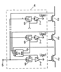
Two preferred exemplary embodiments of the
circuit arrangement according to the invention are
reproduced in Figures 4 and 5. First and second means
(6 and 8) can be provided locally for each switch in
the drive unit (4) (Figure 5). Another variant consists
in that the first and second means (6 and 8) axe
provided centrally only once and all the drivers (7)
and time-delay circuits (9) are driven by these central
first and second means (6 and 8) (Figure 4).
Measurement results of the voltages at three
switches are reproduced in Figures lla-d in the case of
turn-on (Figures lla and llb) and in the case of turn
off (Figures 11c and lld) . As may be seen, the voltage
distribution is clearly better in the case of switching
under control (Figures llb and lld).
Obviously, numerous modifications and
variations of the present invention are possible in
light of the above teachings. It is therefore to be
understood that within the scope of the appendant
claims, the invention may be practised otherwise than
as specifically described herein.