Note: Descriptions are shown in the official language in which they were submitted.
21316~9
FI9-93-057 - 1 -
RETICLE HAVING A NUMBER OF SUBFIELDS
Technical Field
The field of the invention is that of reticles used for
forming patterns on an integrated circuit wafer, including the
field of reticles suitable for use in electron beam systems.
Background Art
In systems that combine or stitch together on the wafer a set
of small subfields on the reticle, as described in S.D. Berger
& J.M. Gibson, APPL. PHYS. LETTERS 57 (2) (1990) 153), there
is the problem of joining up corresponding lines or pattern
features on adjacent subfields. This stitching problem also
exists in any lithographic system wherever fields or subfields
are butted and the features that span the fields or subfields
are stitched together. Imperfect stitching of features can
result in short or open circuits whicll will cause hard
failures in the integrated circuit being formed. Also, if an
overlap is exposed at full strength, the extra intensity will
raise portions of the resist outside the intended area above
threshold, causing "b]ooming" in whicll the feature being
defined has a greater size thall intended. The prior art of
electron-beam direct wrlting exposures has used a technique
called grey splicing in which corresponding features are
overlapped and exposed at 1/2 dose at the boundary with half
the exposure of the main area.
Conse~uently, the art has sought a reticle for stitching that
would offer an acceptable tradeoff between ensuring correct
alignment and mask complexity.
Summary of the Invention
The invention relates to a reticle having, for example, a set
of non-contiguous subfields Whi.CIl may have overlapping rim
portions in which the overlap portiolls of corresponding
213I 669
,~
FI9-93-057 - 2 -
features have a pattern that produces the correct exposure
when the subfields are correctly aligned and minimizes pattern
feature discontinuities whell the subfields are misaligned.
Brief Description of the Drawings
Fig. 1 illustrates in partially pi,ctori,al, partially schematic
style, an e-beam system for use with the invention.
Fig. 2 illustrates an enlarged view of an example of distorted
adjacent subfields on the wafer.
Figs 3, 4, and 5 illustrate details of the application of the
invention.
Fig. 6 illustrates a cross section of a reticle suitable for
use with the invention.
Best Mode of Carrying Out the Invention
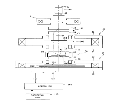
Fig l, shows in parti,ally pictorial, partially schematic form,
- 20 an electron beam system employing an embodiment of the
invention. At the top of the drawiny, electron gun source 10
emits a diverging beam of electrons at a nominal energy of 100
kev downwardly in the Z direction along system axis 102
throuyh illuminatiny aperture 20, llavincJ a nominal dimension
of lmm square in this example. The aperture s'ize is chosen so
that the electron distri,btltloJl across th],s aperture is uniform
within limits sucil tllat tlle i.ntellsity variation across the
subfield on the wafer is acceptab]e.
In order to accommodate the system demalld for a very large
field, the beam will be scanned in steps sequentially across
the surface of retic].e 204. The beam is deflected by
conventiollal deflection means 32 and 34 which have the
capability to defl,ect the beam orthoyollally to the Z-axis in
the X direction (I,eft and rigllt ill the clrawi,ng) and/or in the
Y direction (in ancl out of the p],ane of the paper). The beam
extends do~mwaLd along .seco~l-l axis 104, (for convenience, the
r~
~,,
E . . .
213166~
_ FI9-93-057 ~ 3 -
., .
- beam axis at the nth subfield of the reticle will be referred
to as the "reticle axis"), through a first variable axis lens
denoted generally by the numeral 40 and having upper and lower
pole pieces 42 and 44. Axis shifting yokes 43 and 45 (referred
to generally as axis-shiftillg means) superimpose their fields
over the lens fields generated between the pole pieces 42 and
44 so that the combined fields are azimuthally symmetric about
axis 104 in a region larger than the beam, as is taught in
U.S. patent 4,376,249. With this arrangement, off-axis
aberrations introduced by the lens are substantially reduced,
thereby permitting the use of a large scan field that may
exceed 10mm. Lenses of this type are referred to as variable
axis lenses (VAL), since the optical axis of the lens is
controllably shifted. The use of variable axis lenses provides
high resolution electronic scanning of the reticle and wafer
areas, which is complemented by mechanical scanning of the
reticle and wafer as required to cover the entire chip real
--- estate.
Beam 104 is focused onto reticle 204 by the upper part of lens
40, thereby creatinc) an imac~e of aperture 20 on the reticle
coincident in size with a reticle subfield. Beam 104 strikes
the nth subfield of the reticle 204 and passes along the Z
axis through the bore of pole piece 44. As it passes through
the reticle, the beam is patterned with the information
contained in the subfield. In the case of a conventional
absorbing retic]e, the beam will be essentially absorbed in
thick opaque areas and pass ulldistu3bed through open areas.
Ring-shaped ("doughllut~'~ patterns are .sequentially exposed in
super-position of complementary reticles to compose the
desired feakures as described in H. Boh]e}l et al., Solid state
technol., Sept (1984)).
,,
The lower portion cf lens 40 agai.ll collimates the beam in this
example and, together with cleflector 66, directs the beam to
contrast aperture 70 that performs several functions as
descr.ibed below. Preferably the beam i5 collimated in the
l ~
2131669
FI9-93-057 - ~ -
space between lens 40 and lens 50, in order to reduce
interactions between -the electrons. Collimation is not
required and the term "operating on" the beam will be used to
cover collimating, focusing and defocusing. The lower part of
lens 40 in conjunction with the preceding lenses including the
upper portion of lens 40 focuses an image of source 10 on
aperture 70 as well as col]imating the image of the reticle.
Those skilled in the art will readily understand the
constraints or element position and focal length imposed by
this requirement.
It is an advantageous feature of the invention that the image
of a subfield OII the wafer may be translated from the position
where a full-chip projectioll system would place it. Thus, the
subfields of the reticle can be projected by the system onto
the wafer essentially independently of each other.
Consequently, the requirements to be placed on the reticle
regarding accuracy and stability can be drastically reduced,
as the system can provide small corrections for the position
of each subfield before and even during exposure.
Additionally, the reticle can have pre-distorted features that
compensate for any remaining distortion in the electron
optics. Furthermore, the capability of applying corrections on
a subfield basis (a key advantage of probe-forming systems)
elimina-tes the need for the reticle pattern to be contiguous
over the entire chip area. Consequelltly, a stronger reticle
can be used in which the subfields are physically separated
and reinforcing struts are used to support the reticle and to
resist the distorting effects of tlle heat absorbed by the
reticle such as that illustrated in ~.D. Berger et al., J.
Vac. Sci. & Technol. B 9 (6)(1991) 2996; or in J.A. Liddle et
al., Ibid., P. 3000). The sl]bfields on the wafer are adjusted
in pOsitioll in tlle X-Y plane so that they are contiguous,
using the stitchill~ capability of the system. This stitchinq
will not be perfect, of cou~se, and such a separated-subfield
system has an in]lerellt problem of joining up the images of
adjacent subfields on the wafer.
~L
2131669
FI9-93-057 - 5 -
Deflectors 66 arld 68 perform a translation inverse to that
done above reticle 204 to bring beam 104 back to system axis
102 at aperture 70 and then to hend the beam to final beam 106
(for convenience, the beam axis at the nth subfield image on
the wafer will be referred to as the "wafer axis"), travelling
parallel to axis 102 and on the opposite side from beam 104.
The point at which the beam crosses axis 102 will be referred
to as the pivot point because the beam pivots through that
point as it images various subfields. Variable axis immersion
lens (VAIL) 50 together with the lower half of variable axis
lens 40 focuses beam 106 on to wafer 224, generating a
demagnified image on the wafer of the pattern contained in the
reticle subfield. Lens 50 is a particular form of VAIL in
which a magnetically permeable plate 56 below wafer 224
provides a return path for the magnetic fields that focus the
beam on wafer 224. in general, a VAIL can permit the beam to
pass through. Lens 40 is also a VAIL, since reticle 204 is
immersed in the fie].d. It may be referred to either as a
"dual" VAIL since i.t performs two focusing actions - one to
focus a collimated beam on to reticle 204 and another to
collimate the beam emerging from reticle 204, or it may be
referred to as a "transmissive" VAII" since it transmits the
beam to the next e]ement instead of stopping it.
The axis crossover makes possible some advantageous features
of the inventiorl. One skilled in the art would thi.nk that,
having reduced off-axis aberrations wi.th axis-shifting yokes
43 and 45, it would be sufficient to contin-le beam axis 104
all the way down to wafer ~24, witll on]y a minor correction in
displacement to stitch together the subfields on the wafer.
The addition of any elements invariably introduces aberration,
since no element is perfect. Tllus, one skilled in the art
would prefer to have only a single offset axis and to avoid
the use of additional elements such deflectors 66 and 68. The
addition of def]ectors 66 and 68 and the deflection through
the pivot point, however, effecti.vely decouples the two lens
systems 40 and 50 from each othel, so -that each can have its
~ :
- ~
2131 66~
FI9-93-057 - 6 -
own optical axis independen-tly, with the beam staying 011 these
respective variable axes.
A first advantage of this independer1ce is that the beam can be
steered at all times through one fixed pivot point on the
symmetry axis 102 of the ]ens system at a location that can be
- chosen at will. Thus, there can be a single multi-purpose
- aperture 70 on the pivot point, instead of one aperture for
each subfield. If the beam stayed on the same side of the
system axis, an aperture plate containing one opening for each
subfield would be required. This would not be practical
because extremely stringe11t requirements for accuracy and
stability comparable to those imposed on X-ray masks would
have -to be placed on SUC]I ~ multi-}1ole aperture plate under
continuous hig}1 power electron bombardment. Aperture 70 has
several purposes: to limit the image size of source lO (by
clipping the tails of the electron distribution); to block
electrons strongly scattered in the reticle; to create image
contrast at the target; and to provide a means to sense beam
current for alignment and other corrections. Accordingly, it
will be sometimes referred to as a multi-purpose aperture.
A second advantage is the ability to place elements for
dynamic correction of aberrations (field curvature,
astigmatism, distortion) symmetrically around the fixed pivot
point, so that additior-lal aberrations resulting from the
scanning motion of the beam are minimized because the beam
passes through tl1e corrective elements concentrically.
Lens 40 is also referred to as an immersion lens, in analogy
to optica] lenses, since the object (the reticle) is immersed
in the focussing ~ield defining the lens. Immersion is not
required, and both the physical location along the Z-axis and
the shape of the fields may be tailored. The reticle is not
required to be placed exactly 0l1 ~.he symmetry plane of lens 40
as showr-l in Figure l. Since the lower part of lens 40, in
conjunction witl- lens 50, pLovide.s the overall demagnification
FI9-93-057 7 ~ ~ 3 7 ~ ~ ~
of the system, a di~renl axial position of the reticle may be chosen to op~hlliGe the overall system
performance. For example, the reticle may be placed upsllea~ll and outside the field of lens 40, in
which case both sections of lens 40 will act as one lens.
ELECTRICAL AND MECHANICAL SCANNING
The exposure process requires synchronization of 4 independent sc~nning motions: 1. Electrical beam scan on the reticle
2. Mechanical scan of the reticle
3. Electrical beam scan on the wafer
4. Mechanical scan of the wafer
Both electrical scans can be modified to correct for errors of the mechanical scans of reticle and
wafer, and also to deliberately deviate from the mechanical scans to ~ e overhead times at turn-
around points.
In Fig 1, beam 104 steps over reticle 204 in the X direction illustratively from right to left in the figure
(with beam 106 stepping over wafer 224 ~im~1lt~neously from left to right), while the reticle and wafer
are scanned mechanically in the y direction (in and out of the paper plane). The mechanical motion
is not interrupted for exposures. Blurring of the image due to motion during exposure is avoided by
2 0 deflecting the beam during the exposure (referred to as bucking the stage motion) to compensate for
the stage motion. The beam may be effectively limited to a small range in the Y dimension, say a few
subfield rows, perpendicular to the X-Z plane. There is no need to scan the beam eIectrically by a
large amount in the Y-direction, when a continuously moving stage is used, which accomplishes the
result. However, x and y electrical SC~nning can be combined with a mechanical "step & repeat"
motlon m
.
213166!~
FI9-93-057 - 8 -
order to employ a deflection system having a smaller
deflection than tha-t illustrated here.
Referring now to Fig 2, there is showll an enlarged portion of
a wafer written with the invelltive system, showing
intersection of two adjacent subfields, n and n+l. Note that
lines perpendicular to the edges of the common boundary will
connect at the area in the corners because the subfields
~ overlap there, but such lines will not meet in the center of
_ -- 10 the boundary. Conversely, lines parallel to the boundary may
overlap and short out in the overlap region, while such
parallel lines wilL have an extra margin of separation in the
center area. Consequent:ly, reticles constructed according to
the invention will have an overlap rim extending outside the
nominal dimension so that the images over].ap when the images
are correctly aligned. This overlap will be set empirically to
allow for alignment errors of undistorted subfields, for
distortion errors of correctly positioned subfields, and for
a combination of the two.
One embodiment of the invention is i.llustrated in Fig. 3, in
which lines 3]0 and 320 are from portion of adjacent
- subfields. These lines are meant to align, but are shown
displaced in the drawing for greater clarity. The overlap area
has a checkerboarcl pattern in which elements 316 are~
illustratively opaque and e]ements ~18 are illustratively
transparent. Those skilled in the art will appreciate that
when the aligmnent is correct, there will be no overexposure
and thus no blooming. When the a]ignment is off, there will be
some double exposure and some underexposure, but the
overexposure will be confined to a small area. The
intersection of the shaded areas will not be perfect and will
be deliberately made with a reascnable thickness for
structural reasolls. This is a practical advantage, as overlap
will increase the misaligllmerlt toler.ance.
FI9-93-057 9
The shaded area in Fig. 3 may be an "opaque" portion of the reticle or a transparent portion,
depending on the type of photoresist and the feature being defined. Non-simply connected apertures
(the doughnut problem) may be dealt with by the use of supporting struts by the use of
complementary masks or by the use of a di~l elllial scattering reticle.
In Fig 4, there is shown an improved checkerboard system, in which the shaded areas are transparent
areas 418, with solid or blocking areas 416 shown as lln~h~ded in Fig 4A. In the example, it is
assumed that lines 410 and 420 are the minimllm width for that technology. The apertures in the
checkerboard pattern have been deliberately made sufficiently oversize by an empirical amount
(illustratively 1/3 the width) that will result in that these checkerboard areas print (features below the
miniml Im feature size for a lithography system may print smaller than the reticle image, particularly
when the exposure is optical). Thus, when the alignment is correct, there are overlap areas in which
there will be some double exposure, depending on a number of tool and process parameters, but they
are small, so that some mic~lignmPMt can be tolerated. The overlap areas are the only ones shaded in
Fig. 4B, for clarity in presentation.
Referring now to Fig 5A, a pair of lines 412 and 412' are shown that are intended to join at a subfield
boundary. They are shown displaced in this figure for clarity. Brackets 413 and 413' indicate a
nominal overlap that is designed into the subfields of the reticle. For a nominal alignment error of
2 0 20nm, the subfields should overlap by the distance 413 (illustratively 100nm) in order to ensure that
there are no gaps in connecting lines. Complementary patterned areas having the width of the
nominal overlap are formed at the ends of the lines at the boundaries of subfields. In this particular
embodiment, the pattern is asyllllllellic. Note in Fig 5B that when the lines are correctly aligned, there
is a grid of lines (shown as shaded) that have a double exposure,
' -
'_r
FI9-93-057 10
alternating with rect~n~ r areas that have a single exposure. This arrangement has the advantage
that "blooming" of the pattern from excessive exposure is reduced well below what it would be if the
entire overlap area had a double exposure. Referring now to Fig 5C, there is shown a case in which
there is a lon~ihldin~l displacement along the axis of lines 412 - 412'. It can be seen from the figure
that there is still a substantial overlap that is greater than it would be if a simple checkerboard pattern
were used.
In prior art stencil reticles, the beam passes through open apertures and is totally absorbed by the
"opaque" portions. Unless the reticles are extremely thick, some electrons will pass through the
10 nominal thickness because scattering of electrons is characterized by extensive str~gling Total
absorption may be ensured by the use of extremely thick reticles, but at the cost of scattering on the
walls of apertures and difficulty in supporting the greater mass. In scattering reticles, contrast is
provided by discrimin~ting electrons scal~eled in high-Z thick areas and from those scattered in low-Z
thin areas. There is always considerable scattering from the thin areas because there is a minim~lm
thickness that is required for strength, so that conventional scattering reticles suffer from low contrast
compared with stencil reticles. Stencil reticles and scattering reticles represent two extremes of
reticle design. The former suffers from problems associated with the heat load on the reticle. The
latter suffers from a substantial loss of current at the control aperture even from the "transparent"
areas (som~tim~s referred to herein as "passage" areas) ofthe reticle and will also have heat problems
2 0 because there will be substantial deposition of energy in the high-Z areas of the reticle.
A~
FI9-93-057 11
For convenience in the claims, the term "hindering" and variations thereof will be used as a generic
term to cover absorbing radiation (electrons, ions, or photons) and also scattering radiation (both
elastic and inelastic scattering). The term "resistance to radiation" will be used as a generic term to
cover both thickness and atomic number. As those skilled in the art know, scattering increases as the
material becomes thicker and as a material having a lower atomic number is replaced by a material
having a higher atomic number.
In Fig 6, there is illustrated in cross section a sample reticle constructed according to the invention.
Layer 510 is the main material ofthe reticle, illustratively Silicon. The thickness of layer 510 depends
10 on whether the reticle operates on the absorbing or di~el enlial scattering principle, as the invention
will work with all forms of reticle. Struts 520 and 522 bracket the subfield illustrated. These struts
are separated by a nominal distance indicated by the arrow labelled 502. The nominal usable
dimension of the subfield is indicated by the arrow labelled 504 and is lmm in this example. Struts
520 have a nominal width of about 0.2mm and the thickness of the original wafer (about 0.5mm).
They may be fabricated by conventional etching techniques, e.g. by a plererelllial backside etch.
Aperture 516, represented here in the more common situation of a singly-connected area, is an
opening in layer 510. More complex geometries may be handled by any of the conventional
techniques.
2 0 RETICLE PRE-DISTORTION
To compensate for deflection distortions of the system, the pattern of the reticle can be laid down
pre-distorted in the opposite direction, provided of course, that the system distortions are known and
invariant. For example, in the case of residual barrel distortion in the optical system, the
p
2131669
FI9-93-057 - 12 -
reticle would be pin-cushiol1 sl~aped in the proper amount
varying from subfield to subfield. However, no severe
constraints would have to be placed on the allowable
distortion regarding symmetry or polynomial order. Even non-
linear distortions within a sub-field could thus be dealt
with. Repetitive thermal distortion of the mask under beam
irradiation can be corrected as well as reducing the
requirements for global thermal cllstorti.on.
Althougl1 the invention has been illustL-ated with respect to an
electron beam system, it may also be used with photon, X-ray,
or ion beam systems. ~or example, the reticle need not be
binary and a combination of full and partial exposures may be
- used to pattern the beam. These reticles would have clear
(transmissive) areas, opaque (non-transmissive) areas, and
partially transmissive areas to obtain the fractional (e.g.
l/2) dose required by the overlapping features at the
boundaries. For example, the embodiment of Fig. 3 may be used
with the checkerboard area replaced by a uniform area of
partially transmissive material (transmitting half the
radiation, for example). The mask making process will be more
complex, but there will be the benefit of improved stitching.
The term "radiatioll modulation pattern" will be used as a
general description covering both binary and non-binary
reticles and also covering reticles ~hat pattern the beam by
absorbing incident radiation and those that pattern the beam
by scattering -the incic3ent rac~iatiol1
Those skilled in tlle art wil] rea(lily be ab]e to devise other
embodiments of the invention thall that illustrated and the
, .
scope of the following claims is not meant to be limited to
the embodiments shown.