Note: Descriptions are shown in the official language in which they were submitted.
213~ 7~
CATY SIGNAL SPLITTE~
BACKGR W ND OF THE INYENTION
~ his ~nvention relates to the field of signal splitters for use in
CATY distribution systems, and in other applications in which signals,
having a wide range of frequencies, are distributed across various output
ports. The invention is therefore not necessarily limited tu use in a
CATY system.
At literally thous~nds of locations in a CA~V (community antenna
television) distribution syste~, an incoming signal ~ust be split among
t~o or more outgoing branch circuits. ~he signal splitters that divide
the signal a~ong the outgoing branches must fulfill several challenging
performance criteria. First, the CATV signal has a very broad band~idth,
cur~-ently ranging 'rom 5-552 MHz. In the foreseeable future, the upper
limit will reach 1000 MHz (1 G~z3, so the total band~.~idth will approach
ei~ht octaves of range. At 1 GHz, conventional printed circuit boards
and wire lead components do not perform acceptably.
Secondly, over the frequency range of the signal, the power loss
must be uni~orm, within a small fraction of a decibel. During its trip
from the head-end of the system to a subscriber's home, the signal must
pass through more than a dozen splitters. Any attenuation in the split-
ter w~ll be Inult~pl~ed by the number of splitters in the line.
~ hirdly, the splitters must have ~ery good output return loss. ~his
means that any slgnals flowing back ~rom one of the output branch cir-
cuits should ~e abso~bed by the splitter, and not refl~cted back down th~
branch clrcuit. Signals that are so reflected appear as ~ghost" i~ages
2~3~ ~6~
on a subscriber~s television set.
Fourthly, the splitters must have very good output isolatio~. ~hismeans that a signal entering or exiting one of the output ports should
not appear at another output port. If a signal could travel fr~m one
output port to anot~er, a neighbor's telev;sion reception w~uld be
degraded.
Figure I shows a basic splitter circuit of the prior art. rne cir-
cuit is of the type which produces equal outputs. It is also possible to
provide a circuit with unequal outputs, but the latter circuit is Gutside
the scope of the present ;nvention. The circuit of Figure I includes an
input port and two output ports. Multiple output ports can ~P accom~
modated by constructing binary "trees" each comprising the basic circuit.
That is, each output port of a given signal splitter circuit is connected
to the input port of another identical splitter circuit. In this way, a
plurality of splitter circuits are connected in a cascading arrangement,
so that a single input signal can be split into an arbitrarily large
number of output signals.
If both output ports are loaded with impedance ~0, then the currents
induced by an input voltag~ at point B, flowing through windings N3 and
N4 of ~2, should be equal. If N3=N4, the magnetic fields induced in the
core of T2 by these currents should be equal and npposite, and there ;s
no net voltage between po;nts C and D. The load at point B, as sçen From
the input port, is the parallel combination of the loads on th2 output
ports A and B, or Zo/2. In order to provide correct impedance ~etching,
T1 ls used to transform the input lmpedance by a factnr of Z~ HEnce, the
ratio of turns Nl~N2 to N21 of Tl, should be (2~ 5.
If reflected energy appears at output port A, it is a~sorbed by two
~mpedances ~n series. The first one is the input source 1mpedance ZO,
.-
21317~6
transformed down by a factor of 2 by ~1, result;ng in a load of Zo/2~The second one ;s the load resistor Rl, which is chosen to have impedance
2Zo, transformed down by T2 to ZO/Z, according to the square of the turns
ratio (N3+N4)/N3. These two impedances in series combine to form Z0 ex-
actly, ~or a perfect match.
In the case of reflected energy appearing at output port A, the two
equal series load impedances result in a voltage at point B which is ex-
actly one-half the magnitude, and the same phase, as the voltage at point
C. It is assumed that the windings of T2 have equal numbers of turns,
i.e. N3=N4. Then these windings set the voltage between points B and C
to exactly one-half the voltage between points C and D. Thus, the
voltage at point D is zero, implying that no energy reflected back into
output port A will appear at output port B.
The design of a signal splitter capable of good performance over a
broad frequency range presents substantial problems. While one can ob-
tain load resistors which are nearly ideal over the range of 5-552 MHz,
transformers Tl and ~2 will exhibit significant deviations from the
ideal. To first order, one can consider these dev;ations equivalent to
add;ng impedances in series and in parallel to each transformer winding.
The pariallel impedance represents core magnetization current and losses
in the transformer. Transformer core manufacturers specify the parallel
impedance induced in a one-turn winding oYer the range of operating
frequencles. This parallel impedance can be controlled w;thin a 20%
tolerance, which is quite acceptable ~or a second order effect.
The series impedance, on the other hand~ poses a more difficult
proSlem. The series impedance is laryely due to leakage inductance
resulting from the fact that all of the magnetic field induced by the
-- ~13~
. .
current in each turn of eYery winding on a core does not pass through all
of the other turns. The amount of leakage inductance is determined by
both the core material and the physical layout of the windings. ~rans~
former manufacturers do not specify such effects, and the windings are
made by hand on very tiny cores. Thus, there is wide variatiun in the
series impedance, frequently requiring adjustment in the final product by
manual spreading of the turns.
Several techniques c~n be used to compensate for the equivalent par-
allel impedance introduced by Tl and T2. First, identical cores can be
used for Tl and ~2, and wind;ngs N2, N3, and N4 can all be set equal. In
this case, the critical output isolation, between output ports A and B,
will be mainta;ned independent of the exact value of the parallel core
losses.
Secondly, one can take advantage of the fact that the parallel core
loss impedance of good wideband ferrite core material is almost perfectly
resistive and fairly constant over most of its intended bandwidth. Thus,
the value of the load resistor Rl can be increased and the input matthing
transformer ratio (Nl~N2)~N7 can be decreased to compensate for the addi-
tion of this parallel resistance.
~ he above-described compensation teshnique can be extended to deal
with the case where N2 is not chosen to be equal to N3 and N4. The
primary limitation to such compensation arises from the more severe lim-
~tations imposed by performance degradat;on due to series leakage in-
ductance.
Compensation for the equivalent series impedance ;ntroduced by leak-
age inductance in Tl and ~2 is the single most important determinant of
splitter performance. Figure 2 shows a typ;cal prior art circu;t which
attempts to eompensate ~or leakage inductance. Since the leakage imped-
':i ~,,.,.",.i~.... ,.. . , ~. .
`` 2~317~
ance is largely inductive, the classical s~lution ~as to add capacitorsto ground so as to form, effectively, ~ultiple LC transmissivn line half-
sections with the distributed series inductance. ~he half-sect;ons
should have opposlng or;entations, and each should have a natural imped-
ance equal to the circuit impedance at that point. This means that the
;mpedance should be Zo=Ls/C, where Ls is the leakage inductance. The
capacitance of Cl can be viewed as the sum of three capacitances in par-
allel, one capacitance form;ng a transm;ssion l;ne half sect;on w;th the
leakage inductance of Tl, and the other two forming transmission line
half sect;ons with the leakage inductances of the tWD halves of T2. The
capacitance of the output connectors to yround also forms a transmission
line half section with a part of the series leakage inductances of ~2.
A major practical limitation to transmissi~n line leakage inductance
compensation, at frequencies over 300-500 MHz is the lead inductance of
Cl. Frequently, Cl is implemented as several capacitors in parallel, to
reduce this parasitic effect.
~ he pr;or art circuit of Figure 2 compensates ~or the output isola-
t;on degradat;on due to the leakage inductance of T2 by adding inductors
Ll and L2 ;n series with the load resistor Rl. A s;gnal orig;nating at
one output port flows through two parallel paths, one path passing
through T2 and the other path passing through Ll, L2 and R1, to reach the
other output port. ~he signals in these paths are 180- out of phase, due
tu the action of transformer T2. The magnitude of these signals are ad-
justed to be equal so that the signals therefore cancel. ~hus, no signal
originating at one nf the output ports appears at the other output port.
However, the circuit of Figure 2 has the disad~antage that when the
high frequency attenuation is balanced in the two paths, the phase shift
. ,~,; .;' ~ " ~ " ~ ",
`
3 ~ 7 ~
~ ~.
through transformer T~ is significantly greater than that of the path
containing Ll, L2; and Rl. This effect limits the ability of the circuit
to prov;de th~ des;red signal isolation. ~his effect is due to the fact
that one of the signal paths, namely the path through T2, cDntains two
transmission line ha-f-sections. These half-sections ;ntroduce the un-
wanted rapid phase shift.
The present invention prov;des a signal splitter which hias all of
the desirable characteristics outlined aboYe, namely, sat;sfactory opera~
t;on across a wide bandwidth, output isolation, and acceptable ;mpedance
matching, but which also easily compensates for leakage inductance in the
transformer. The circuit of the present inVentiDn is also especially
easy to realize using surface mount tecnnology ~SMT), which ;s the tech-
nique of choice when dealing with high frequency siynals.
SUMMARY OF THE INYENrlON
In the signal splitter of the present i~vention, there is an input
port and two output ports. A s;gnal ~rom the input port is connected to
the center tap of an autotransformer, the e~ds of the cDupled inductors
forming the autotransformer being connected to the output ports. A
bridge load circuit, comprising an induct~r connected in parallel with a
load, is connected t~ the autotransformer by inductive coupling only.
There is no other connection between th~ bridge load circuit and the sig-
nal splitter.
The br;dge load c;rcuit, through indu~tive coupling ~o the auto-
transformer wind;ngs, effect;vely pr~vides a Zo/2 load between the center
tap of the autotransformer and the output p~rts. The transformed load in
series with the Zo/2 transformed input source impedance provides the
~ ':
~ r~ ". .~.` ,. .,. '", .~. . :.~., ' ~
:~ 2~ 7~ ~
desired isolation of the output ports, as desçribed in the classical
splitter design.
More sign;ficantly, because the bridge load circuit is coupled only
;nduct;vely to the autotransformer, the series leakage inductance of the
autotransformer wind;ngs lies outside the path of the bridgc load cir-
cuit. Thus, the leakage inductance does not cause a high frequency phase
shift problem, as was true in the circuits of the prior art. Elimination
of the inductors in series with the load resistor makes it signif;cantly
eas;er to ;mplement the present circu;t us;ng surface mount technology
(SMT). Input and output impedances can be matched by si~ple choice of
~optional) inductances placed in series with the ou~put ports and capaci-
tances, connected between the output ports and ground~
The present invention therefore has the primary object of providing
a signal splitter capable ~f uniform op~ration through a wide range of
frequencies.
The invention has the further object of providing a signal splitter
in which signals from one output port are not transmittPd into another
output port.
The invention has the further object of provid;ng a signal splitter
in which s;gnals flowing back from an output branch circuit are not re-
flected back into the branch circuit.
The invent;on has the further object of providing a signal splitter
which can conveniently be made using surface mount technology.
The invention has the further object of overcoming the problems as-
soc~ated with leakage inductance in autotrans~ormers operating at
frequencies up to 1 ~z.
The inventian has the further object of providiny a signal splitter
:` 2~7~
in which input and output impedances can be easily matched.
The invent;on has the further object of providing a signal splitter
in which impedance matching ;s ;ndependent of the means for overco~ing
phase shifts due to leakage inductance.
- The person skilled in the art will recognize other objects anc ad-
vantages of the present invention, from a reading of the following brief
descript;on of the draw;ngs, the deta;led description of the invention,
~nd the appended clai~s.
~RIEF DESCRIPTION OF THE DRA~!NGS
F;gure I provides a schematic diagram of a signal splitter circuit
of the prior art.
Figure 2 provides a schematic diayram of another signal splitter
circuit of the prior art, wherein the circuit provides so~e compenseti~n
for leakage inductance at high frequPncies.
Figure 3 provides a schematic diagram of the signal spl;tter circuit
of the present invention. .
'
,
. .
, ,:
21~1 7~
DE~AILED DESCRIPTION_OF THE INVENTION
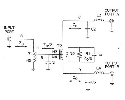
Figure 3 shows a schematic diagram of a circuit made according to
the present invention. In the circu;t of Figure 3, a signal appl;ed at
the input port appears at output ports A and B. Autotransformer Tl func-
tions in a similar manner to autotransformers Tl in Figures 1 and 2.
Thus, the labeled impedanc'es (ZO) are similar to those obtained in the
prior figures. Components of Figure 3 which have the same function as
components of Figures 1 and 2 are labeled with similar reference
numerals~ '
As in the prior art, the signals appearing at the output ports can
be connected to the inputs of similar splitter circ~its. Thus, a plural-
ity of identical splitter circuits can be cascaded together, 50 that a
head-end signal is split ;nto a large number of output signals
The signal splitter of Figure 3 includes a bridge load circuit
which, in the embodiment of Figure 3, comprises a transformer winding N5
lnominally chosen to have the same number of turns as the windings N3 and
N4], load resistor Rl, having a value Zo/2, and capacitor C4, connected
in parallel tD Rl as shown. In the preferred embodiment, th~ bridge load
circuit has no connection to the signal splitter circuit except through
the ;nductive coupling Df wind;ng N5 to windi1lgs N3 and N4. In other
words, the bridge load circuit "floats~7 because it is not directly con-
nected to the main circuit.
Due to the ~agnetic coupling of N~ with N3 and N4, the circuit
"sees" resistor Rl as if it were connected directly across N3 or N4. For
this reasnn, in the arrangement of Figure 3, there are, in effect, two
series load impedances applied to ea~b output port, namely, the s~urce
impedance, transformed by a factor of 2 by Tl to Zo/2, and the load im-
~ .
-21317~
pedance Rl, having a value of Zo/2, coupled to either N3 or N4 without
impedance scaling. When these two ;mpedances are chosen to be equal, and
when N3 is chosen to equal N4, a signal originating at one output port
does not appear at the other output port.
A major difference between the circuit of Figure 2 and the circuit
¦ of Flgure 3 ;s that, because of the inductive coupling of the bridge load
I : circuit in Figure 3, the series leakage ;nductances of wind;ngs N3 and N4
are outside of the bridge load circuit. ~he result is that the phase
shifts which plague the circuit of Figure 2 are not a problem in the cir-
cuit of Figure 3.
Capacitance C4 compensates for the series leakage inductance in N5
and the windings N3 or N4 of transformer ~2 in exactly the same manner
that Cl compensates for leakage inductance of windings Nl and N2 of
transformer Tl. Both of these compensations function identically to in-
sure that the transformed Zo/2 load impedances are equal over the fre-
quency range of the splitter. It is easiy to insure that these trans-
formed load impedances are equal, balancing the bridge and preventing
signalsi enter;ng one output port from appearing at the other port. Note,
however, that C4 can be omitted ;f the values of the other circuit compo-
nents are correctly chosen.
In the circuit of Figure 3, capacitors Cl, C2, and C3, and inductors
L3 and L4 together comprise the components which provide satisfactory
impedance matching at both the input and output ports. In particular,
since the output port connectors commonly used in CATV systems have
capacitance with respect to ground, inductors L3 and L4 can be used to
compensate. One could also compensate for such capacitance by varying
Cl9 but one cannot achieve satisfactory compensat;an by changistg Cl
alone, without dtsturbing the output isolation. It turns out that L3, C2
1~
~,-~., ,-,,, ~-.~i:,;~ ,i;i, ~ ':' ' '',. ' '' '~':' `~
. ?
1~; ; ' '.'.~'~,;, '.,. ,',' ~' ' ~ ' . ;~ i " !.~. " i
. 2~317~
(~r part thereof), and the output capacitance of the output port connec-
tor tog2ther form a pi transmission line section; a si~ilar statement
holds true ~or L4, C3, and the capaeitance of the connector of output
port B. Note also that each of C2 and C3 can be visualized as two
I capacitors connected in parallel, with one of the capacitors being used
¦ to compensate for unequal leakage inductances of T1 and T2.
The circuit designer has direct control of the values of Cl, C2, C3,
L3, and L4. ~hus, the designer has control of at least one element in
each transmission line half-section. Thus, ;t is easy to choose values
for these components which will provid~ optimum impedance matching and,
simulteneously, optimum output isolation. Moreover, since the series
leaka~ impedance of the windings of ~2 are not in the path of Rl, the
circuit completely eliminates the high frequency phase sh;ft problem.
The load resistor R1 can have much lower impedance, a~d is easier to
realize at high frequencies. The relatively high value inductors Ll and
L2 of Figure 2 are eliminated; the inductors L3 and L4 of Figure 3 are
much smaller, and can be reall~ed as simple printed circuit board strip-
line inductors.
rne preferred design of T2 is to use the same number of turns for
the N3, N4, and N5 windings. ~he turns of these winding5 can then be
w~und tri-fillar (intersper5ed) which significantly reduces the series
leakage inductances of these windings.
In the sase wherein the ~utput impedances are equ~l, and wherein
N3'N4=N5, the value of Rl is chosen to be 2 J 2. In tbe m~re general
case, ~herein N3 N4, but N5 does not necessar;ly equal N3~ the value of
Rl is given as (Zo/2)(N~/N3)~, which reduces to Z~/2 when N3~N5. If the
output impedances are not equal, Rl must be chosen such that the DUtpUt
..
11
2~L3~7~ :
impedance matches the input impedance.
The signal splitter c;rcuit of the present invention is 2specially
suited for implementation ;n surface mDunt technology (SMT). For ~re-
quencies of 1 GHz, SMT is a virtual necessity for acceptable realization
of many circuit components. SMT significantly reduces the size of the
active circuit, and minimizes the use of inductive components. It is
especially important tc use an SMT component in realizing Cl, where the
lead inductance of through-hole components is unacceptable even at 500
MHz. The improved impedance consistency of SMT construction signi~icant-
ly reduces the need for manual adjustment of the circuit. ~o achieve
this advantage of SMT, all relat;vely h;gh-value ;nductors, wh;ch cannot
be practically implemented in SMT, have been eliminated in the present
invention. ~he two remaining inductors (L3 and L4) are of low value and
are in non-critical locations. If shielding is not critical, these in-
ductors can even be implemented by meander or PCB transmission line seg-
ments.
In mounting transformer cores to ~ circuit board using SMT, it has
been found advantageous to mount the cores to the underside of the board.
:.~
However, at the high frequencies of interest here, the cores are both
inductive and capacitive, and so it becomes necessary to control the
dielectr;c between the winding and the circuit board. A preferred means ~;
of mounting the core to the circuit boiard is to use a p;ece of double-
sided ridged foam adhesive, of the type commonly used in mounting pic-
tures to walls. The foam adhesive makes it possible to mount the core to
the circuit board with consistent ~pacin~, and also provides a diclectric
having a known and low dielectric constant, for the capacitor defined by
the core and the circu;t board.
In a modification of the present invention, it i5i also possible to
12 .
. . ~ r ~ . . . ; i
,; ~ i '; ''
21317 ~
provide a bridge load circuit which is only partially "floakinga. In
this alternative, one could ground either end of the bridge load circuit,
while maintaining the inductive coupling described abcve. In this case,
there is still no direct path from one output port, through the load, and
to the other output port.
While the invention has been described with respect to particular
embodiments, many further Yariat;ons are possible. Such modifications as
will be apparent tD those skilled in the art should be considered within
the spirit and scope of the following claims.
; ~:
. : .:
~: ~
:::
..,
:
13 . .
; ~ . " ", ~
A
. ~ "