Note: Descriptions are shown in the official language in which they were submitted.
PCTlU~93100362
WO 94117625 ~
1
TITLE OF THE INVENTION
DIGITAL ELECTRONIC EXPOSURE CONTROL
BACKGROUND OF TI-iE INVENTION
1. Field Of The Invention
5. The present invention relates generally to imaging systems or
camera systems (such as photographic and video cameras), and more
particularly to exposure controls for imaging systems/camera systems.
2. Related Art
The use of charge coupled devices (CCDs) in camera imagers has
enabled the production of smaller and more durable camera imagers.
Much effort has been spent in developing ire control systems for
effectively controlling imager sensitivity to incident light on the imager '
(that is, for controlling the amount of charge a CCD accumulates during
a field integration period). Exposure control systems which regulate CCD
exposure sensitivity, such that picture quality is unaffected by changing
environmental lighting conditions, are desired. Such exposure control
systems greatly expand the dynamic range of performance of CCD-based
imagers, thereby increasing the commercial market for CCD-based camera
imagers. Herein, light refers to visible and non-visible light.
In many conventional CCD-based camera imagers, the exposure
control systems are implemented using mechanical devices. Such
mechanical devices include a mechanical iris and/or a mechanical shutter
wheel. The most common implementation, the mechanical iris, varies the
rate at which the CCD receives photons. 'Ifie mechanical shutter varies
the amount of time during which the CCD receives photons.
WO 94117625 PCTIUS93100362
Such exposure control systems are flawed, however, since
mechanical devices have a relatively low reliability, slow response time,
and increase the size and cost of the lens. Additionally, such exposure
control systems are flawed since the ~ase of mechanical devices increases
the technical difficulty in the areas of loop stability and design transition
between different lenses.
In some tube based cameras, such as some "VmIC:ON' cameras,
the exposure control systems can be non-mechanical in nature. Such
exposure control systems automatically control imager sensitivity by
controlling the voltage on the tube's target electrode.
Since vacuum tube type imagers arc larger and less rugged than
solid state imagers, solid state imager based cameras such as CCD
cameras are being used in place of the older tube technology ~ based
cameras. - In order to match all performance aspects of tube based
cameras with OCD based cameras, a non-mechanical exposure control
system for controlling OCD sensitivity is required. Due to the different
nature of the solid-state imager to the tube imager, the same electronic
exposure control technique as the tube-based imager cannot be utilized
for the solid-state imagers. There is no analogous sensitivity altering
technique for the solid-state imager similar to the tube's target electrode
voltage. Therefore, a different technique to achieve similar electronic
light control for the solid state imager is required.
Several major CGD suppliers offer on-chip shuttering options. On-
chip shuttering is the electronic process that allows accumulated charge
in the charge storage wells to be dumped before the end of the normal
integration time. This allows the exposure interval per.imaging cycle to
be varied, enabling high speed stop action effects. This change in
exposure interval also results in a corresponding change in sensor
sensitivity. G~rrently, light control systems based solely on on-chip
shuttering do not exist. This is due to the many restrictions imposed due
PCTIUS93/00362
WO 94117625
213180
_.,_
to CCD timing constraints and undesirable imaging side-effects upon
application of an electronically variable exposure setting.
'Thus, a high performance exposure control system for effectively
controlling CCD sensitivity is required.
SUT~IMARY OF THE INVENTION
The present invention is directed to a system and method for
electronically and automatically controlling charge coupled device (CCD)
light sensitivity to achieve optimum imager performance under varying
light conditions. The present invention applies to color and monochrome,
as well as non-visible applications.
The present invention does not control CCD light sensitivity by
regulating the amount of photons incident on the CCD. Also, the present
invention does not use electromechanical devices to control CCD light
sensitivity.
Instead, the present invention controls CCD light sensitivity by
electrically controlling a CCD such that the CCD discharges tht charge
resultant from incident light for a percentage of a field integration period.
In other words, the present invention electronically varies the CCD's
exposure time.
The present invention operates as follows. First, the present
invention calculates a new optimum exposure time for the next field
integration period based on the present video output level (which is a
product of .the present amount of light incident on the CCD and the
present exposure period). Second, the present invention electrically
causes the CCD to discard charge accumulated by the CCD during the
field integration period, except during a portion of the field integration
period desned by the new exposure time.
WO 94/17625 PCTlUS93/00362
'x'1318 ~ 5 _
., _
The present invention calculates the new exposure time as follows.
First, the present invention determines the measured video signal level
from the imager's video output, which represents the charge accumulated
in the CCD. Second, the present invention calculates a correction factor
S by comparing the measured video signal level to the desired video signal
level. 'lfiird, the present invention calculates the new exposure time by
using the correction factor to modify an old exposure time. Fourth, the
present invention incorporates hysteresis to prevent electronic exposure
"hunting,' otherwise resulting in observable video flicker. Fifth, the
present invention applies the dump pulses only during periods when their
application will not cause the CCD imager to produce unwanted video
side-effects.
The present invention electrically causes the CCD to discard charge
acxumulated by the CCD as follows. First, the present invention
determines the number of dump pulses needed during a discrete mode to
attain the new exposure time. Second, the present invention determines
the number of dump intervals needed during a continuous mode to attain
the new exposure time. Third, the present invention generates a
waveform having the dump pulses and dump intervals.
Further features and advantages of the present invention, as well
as the structure and operation of various embodiments of the present
invention, are described in detail below with reference to the
accompanying drawings. In the drawings, like reference numbers indicate
identical or functionally similar elements. Additionally, the left-most digit
of a reference number identifies the drawing in which the reference
number first appears.
..;,... ., . ;. ~.~,'.. " ~;.~.... .. .. ~~~ ~.. '~':.'.~._. .':':l
,~.,..:.~...... 'i'..,. ...~~'.~.. ,:..ns';;: .,y ....,::.:.:.... ..
WO 94!17625 PCTIUS93I00362 '
2131805
_>_
BRIEF DESCRIPTION OF THE DRAWINGS
The present invention will be described with reference to the '
accompanying drawings, wherein:
Figure 1 presents a flowchart which illustrates the operation of an
S exposure control system of the present invention.
Figure 2 illustrates a video camera according to the present
invention.
Figure 3 illustrates a synchronizing signal waveform.
Figure 4A illustrates a time line which shows a field integration
rind. ~
Figures 4B and 4C illustrate examples of a modified charge
dumping signal aooording to the present invention.
Figure 5 illustrates a strucd~ral block diagram of the exposure
control system of the present invention.
Figure 6 fllustrates a structural diagram of an EPLD.
Figure 7 fllustrates a structural diagram of a logic block 612 of the
EPLD. . .
Figure 8 illustrates a structural diagram of a logic block 614 of the
EPLD.
Figure 9 illustrates a correction factor versus A/D output graph.
DETAILED DESCRIPTION OF THE PREFERRED EMBODIMENTS
1. Sv,~nchronizine Signal Wavefontn
The present invention may be better understood by first
considering a synchronizing signal waveform 301, as illustrated in
Figure 3. The synchronizing signal waveform 301 is used to reference the
various scanning intervals of electronic imaging systems. Solid state
WO 94!17625 FCT/US93I00362
13105
imagers, such as video cameras, operate according to the synchronizing
signal waveform 301. Electronic image displays, such as CRTs, trace
images in synchronization to this signal 301.
The synchronizing signal waveform 301 comprises periodic intervals
called field integration periods 302. A single field is traced during each
field integration period 302. '
Each hold integration period 302 includes a picture interval 304
and a vertical blanking interval 310. The picture interval 304 includes
active video intervals 306 and horizontal blanking intervals 308.
During the active video intervals 306, lines of a field axe traced by
an electron beam associated with a video display. During the horizontal
blanking intervals 308, the electron beam intensity is blanked while the
beam is positioned to the beginning of the neact line of the field. During
the vertical blanlong interval 310, the electron beam intensity is,blanked
whUe the beam is positioned. to the start of the neat field.
In a preferred embodiment of the present invention, the field
integrRtion period 302 for C~CDs is 1/60th of a second (appraoomately 16.7
msec). The picture interval 304 lasts approximately 15.6 msec. The . .
vertical blanking interval 310 lasts approximately 1.1 msec. Each active
video interval 306 lasts approximately 53 usec.
A common type of synchronizing signal waveform 301 is described
in many publicly available documents, such as EIA RS-170 and EIA-
RS-343. EIA RS-170 and EIA-RS-343 are standards developed by the
Electronic Industries Association (EIA).
2. Overview of the Present Invention
This suction presents an Overview of the structure and operation of
the present imrention.
PCT/US93100362
WO 94/17625
2131805
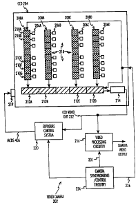
Figure 2 illustrates a video camera 202 according to the present ,
invention. The video camera 202 includes a charge coupled device (CCD)
204, video signal processing circuitry 216, camera synehronizing/control
circuitry 224, and an exposure control system 220. The CCD 204 includes
photosensitive areas 206, vertical shift register areas 208, horizontal shift
registers 212, a video output stage 214, a substrate region 218, and a
substrate pin 219.
'The photosensitive areas 206 and vertical transfer registers 208 are
formed in rows 210. At the conclusion of each field integration period, '"
the charge accumulated in the photosensitive areas 206 is transferred to
the vertical shift register area 208. During the neat field integration
period, the charge transferred to the vertical shift register 208 is
transferred sequentially domoward one row 210, at a time, with the
bottom row 2106 mewing to the horizontal shift register 212. This occurs
at the TV line rate, once appraaomately every 63.5 microseconds for the
FIA RS-170, 525 line example. During each 63.5 microsecond line
period, the horizontal shift register 212 is shifted rightward in similar
fashion at a clock rate sufficient to move all charge out before the next
vertical dump, 63.5 microseconds later. The charge is shifted into the
video output circuit 214, which converts the charge to a voltage. Due to
the clocking of the horizontal shift register 212, a serial stream of
voltages, representing each individual photosite charge, is serially output,
forming the video signal in a standardized format, EIA-RS-170, for
example.
The video camera 202 operates generally as follows.
During a field integration period 302, the photosensitive areas 206
receive photons which originate from outside the video camera 202. The
photons represent an image that is being recorded.
The photosensitive areas 206 convert the photons to electrical
charge. This charge is transferred once per TV field to the adjacent
WO 94117625 PCT/US93100362 ,
,~31~~~
2 -~-
vertical shift register areas 208. The photosensitive areas 206 store (or
accumulate or integrate) the charge during the field integration period.
In conventional video cameras, the photosensitive areas accumulate
charge during the entire field integration period 302. In other words, the
exposure time (that is, the percentage of the field integration period 302
during which the charge storage areas accumulate charge) is constant.
The conventional video cameras achieve light sensitivity by using light
control systems which regulate the amount of photons incident on the ,
CCDs. .
According to the present invention, however, the amount of
photons incident on the GCD is not regulated. Additionally, the
photosensitive areas 206 accumulate charge for only a portion of the field
integration period 302 (that is, the exposure time is not constant). The
video camera 202 of the present invention achieves eapasure sensitivity by
using the exposure control system 220 to vary the exposure time. In other
words, the exposure control system 220 determines the pordon of the
picture interval 304 during which the photosensit?ve areas 206 accumulate
charge.
Specifically, the exposure control system 220 generates a modified
charge dumping signal (MCDS) 406 which is applied to the substrate pin
219 of the ~CCD 204. According to a preferred embodiment of the
present invention, the charge accumulated in the photosensitive areas 206
is discarded (or dumped) to a drain-off region (represented by the
substrate region 2I8) when the modified charge dumping signal 406 has
a low voltage value. Then, the photosensitive areas 206 restart
acxumulating charge. Such charge accumulation continues until the
modified charge dumping signal 406 goes low again, or until the field
integration period 302 e~cpires. Thus, the duty cycle of me mocunea
charge dumping signal 406 (as controlled by the exposure control system
WO 94117525 PCTlUS93100352
_21318U~ ~.
. .. .",
220) determines the percentage of the field integration period 302 during
which the photosensitive areas 206 accumulate charge.
After the field integration period 302 expires, the charge stored in
the photosensitive areas 206 is transferred to the vertical shift
S registers 208. During the subsequent field integration period 302, the
charge just transferred into the vertical shift register is sequentially
shifted
downward, row by row, into the horizontal shift register 212. For
example, the charge in row 210A is moved into row 2108, 2018 into
210C, etc., and row 2106 into horizontal shift register 212.
The charge in the shift register 212 is sequentially shifted out,
column-by-column, to the video output circuit 214. For example, the
charge in column 212D is shifted out to the video output circuit 214.
Simultaneously, the charge in cohmnn 212C is shifted to column 212D.
This contimies until the charge in cohmnn 212A is shifted through the
register 212 and out to the video output circuit 214.
The video output circuit 214 generates a video out signal 222 by " .
converting the electrical charges from the shift register 212 into a
proportional voltage for each pixel. Thus, the video out signal 222 is a ~ ; ,
.
series of voltages corresponding to the electrical charges accumulated in
each pixel.
The video out signal 222 is sent to the video signal processing
circuitry 216 for further processing. The structure and operation of the
video signal processing circuitry 216 is well lmown.
This video out signal 222 is also sent to the exposure control
system 220. Based on the video out signal 222, the exposure control
system 220 generates the modified charge dumping signal 406 for the nwct
field integration period 302. 'Thus, the present invention includes a
feedback loop (which includes the exposure control system 220) for
controlling the light sensitivity of the CCD 204.
WO 94117625 PCTIUS93I00362
2,~3~g05
The camera synchronizing/control circuitry 224 orchestrates all of
the charge accumulation and transfers described above, synchronizing all
functions to yield the serial video stream in conformance to a video
standard, such as EIA-RS-170. It gene>:ates CCD transfer clocks 226, as
S well as the video synchronizing signal~'waveform 301.
By using the charge acxumulated during the current field
integration period to control the amount of charge allowed to be
accumulated during the next field integration period, the exposure control
system 220 of the present invention minimizes changes in picture quality
due to changes in environmental lighting conditions.
The manner in which the exposure control system 220 generates
the modified charge dumping signal 406 is described below.
3. ~ and plementation Considerations
'Ibis section describes considerations which affected the design and
implementation of the exposure control system 220 of the present
invention.
3.1. Discrete Mode
Dumping charge during the active video intervals 306 creates
increased signal pedestals, resulting in undesirable picture side-effects
such as dark areas on the picture. Such increased signal pedestals reduces
picture ~ quality. Thus, the exposure control system 220 does not cause
accumulated charge to be dumped during the active video intervals 306.
' ~ Rather, with regard to the picture interval 304, the exposure control
system 220 causes accumulated charge to be dumped only during the
horizontal blanking intervals 308.
PCTIUS93100362
WO 94/17625
21318~~
- Il -
The exposure control system 220 is said to be in a "discrete mode"
while in the picture interval 304 since the restriction to dump during only
the horizontal blanking intervals 308 results in discrete steps in exposure
time. These discrete steps are equal to the duration of each of the active
S video intervals 306 (that is, approximately 63.5 usec for the EIA-RS-170, '
525 line example).
If the exposure control system 220 operated in only the discrete
mode, then the exposure control system 220 would achieve an exposure
time range from 63.5 usec (that is, a single step or a single line) to 1/60t11
of a second (that is, the entire field integration period 302) in increments
of 63.5 usec.
However, there is a drawback to operating in only the discrete
mode. This drawback is illustrated by Equation 1, which quantifies the
percentage change in exposure time, In Equation 1, O equals an old
exposure time and N equals a new exposure time. Both O and N are
integral multiples of 63.5 uses.
9O Change in Exposure Time = 100 * ( (N - O)/O )
Equation 1
Suppose O equals three lines (that is, 190.5 usec) before the end
of its field integration period (that is, the charge is accumulated only
during the three discrete steps before the end of the field integration
period -- all other charge during the field integration period is dumped).
Also suppose that N equals four lines (that is,, 254 usec). According to
this scenario, the percxntage change in exposure time. is 3396. A large
percentage change in e~cposure time wUl result in noticxable video output
level (brightness) steps occurring on the resultant displayed image,
It has been experimentally determined that a percentage change in
exposure time by more than 3 to 496 is noticeable and sometimes
WO 94!17625 PCTIUS93/00362
2,~3~g~5
- 1? -
distracting to the observer. Thus, there are drawbacks with operating
exclusively in the discrete mode.
3.2. Continuous Mode
Dumping charge during the vertical blanking interval 310 does not
S create increased signal pedestals because the video is blanked during this
period. Thus, the exposure control system 220 i$ allowed to cause the
accumulated charge to be continuously dumped during the vertical
blanking interval 310 with much finer resolution than the 63.5 usec steps
of the discrete mode. Consequently, the exposure control system 220 is
said to be in a "continuous mode" while in the vertical blanking interval
310 since accumulated charge may be continuously dumped.
The ability to continuously dump charge during the continuous
..
mode onsets the drawbacks of the discrete mode. Specifically, without
the continuous mode, the last charge dump during the discrete mode
1S results in a percentage change in exposure time of SO~Yo. With the
continuous mode, however, the last charge dump during the discrete
mode results in a much smaller percentage change in exposure time.
According to the present invention, the exposure control system
220 may cause accumulated charge to be dumped for a period
encompassing either part of the discrete time interval, the entire discrete
time interval, all of the discrete and part of the continuous time interval,
or all of the discrete and all of the continuous time intervals. 'The
exposure control system 220 ' generates the modified charge dumping
signal 406 to control when and to what extent the accumulated charge is
2S duped.
Figures 4A, 4B, and 4C illustrate examples of the modified charge
dumping signal 406. Specifically, Figure 4A illustrates a time line which
shows a field integration period 402. Figures 4B and 4C illustrate
WO 94117625 PCTIUS93100362
~:~3~~0~
examples of the modified charge dumping signal 406 which may be
compared by reference to the time line in Figure 4A.
In Figure 4B, the exposure control system 220 has generated a
modified charge dumping signal 406 such that accumulated charge is
dumped only during a portion of the discrete mode. As shown a Figure
4B, the modified charge dumping signal 406 contains four low pulses
during the discrete mode. Thus, charge accumulated during four lines
(that is, 254 usec) is dumped. Consequently, the total exposure time is
approximately 16.4 cosec.
In Figure 4C, the exposure control system 220 has generated a
modified charge dumping signal 406 such that accumulated charge is
dumped during the entire discrete mode and the beginning of the
continuous mode. Although not explicitly shown in Figure 4C, the
modised charge dumping signal 406 in Figure 4C contains 249 low pulses
during the di9crete mode and 442 low increments during the continuous
mode (in other words, the modified charge dumping signal 406 is low for
approximately 486 usec during the continuous mode). Thus, the total
exposure time is 369 usec.
4. Fxoosure Control System
According to the preferred embodiment of the present invention,
the e~cposure control system 220 is implemented wing a digital approach.
The use of a digital implementation is advantageous for a number of
reasons.
First, the hybrid nature of the exposure control system 220 due to
its two modes of operation (that is, dixrete and continuous) imposed tight
restrictions upon response time and other loop stability criteria. A digital
implementation, unlike an analog implementation, is well suited to satisfy
such restrictions.
WO 94/17625 PCT/US93/00362
_ l :l _
Second, without hysteresis, the exposure control system 22U will
attempt to continuously hunt between light levels because the discrete
nature of exposure time results in the inability to achieve totally optimum
exposure time. This inability results in an instantaneous exposure error.
S White this small exposure error will not directly impact picture quality, it
will, as a secondary effect, cause the exposure loop to alternate exposure
.a
times to the discrete value on either side of the optimal value. This
"hunting" action manifests itself as a visible and sometimes distracting ~ .
flicker in the output video image.
According to the present invention, the exposure control system
220 includes a hysteresis for avoiding this problem. An analog
implementation of hysteresis for this control loop would require a
significant amount of circuitry and require careful adjustment A digital
implementation can easily incorporate this hystcresis. Also, a digital
implementation can implement this hysteresis without the use of select at-
test resistors or potentiometers (which might be required if an analog
approach were used). Thus, the digital implementation facilitates high
volume. production since tuning and select at-test requirements are not
required (conversely, an analog approach requiring the use of select-at-
test resistors or potentiometers would not be suited for high volume
production).
Figure 5 illustrates a structural block diagram of the exposure
control system 220. The exposure control system 220 includes an AC
couplel~'ET black level clamp 502, a RC filter 504, an amplifier (AMP)
506, an analog to digital (A to D) converter 508, a programmable read
only memory (PROM) 510, a latch 512, and an Erasable Programmable
Logic DGVICe (EPLD) 514. . '
Aooording to the preferred embodiment of the present invention,
the AMP 506 may be any general purpose op-amp with a gain-bandwidth
product compah'bie with video signals (15 MHz in this example). The A
WO 94/17625 PCTNS93100362
2.31805
_,;_
to D converter 508 should have a minimum resolution of 6 bits and a
conversion time of less than 90 microseconds.
The PROM 534 may be any type of 32K x 8 EPROM, PROM,
ROM, or OTP. The combined A to D conversion time and EPROM
S access time must be under 90 microseconds.
The EPLD 514 inner circuitry is a schematic based design using a
hierarchal approach consisting of blocks of circuit primitives. Thus, this
design can be easily translated between the various programmable devices
and gate arrays. The EPLD 514 is available from Alters and Cypress.
Figure 1 presents a flowchart which illustrates the operation of the
exposure control system 220. Figure 1 is described below with reference
to the digital circuit shown in Figure 5. Note, however, that the operation
of the eacposure control system 220 as illustrated in Figure 1 may be
implemented using different circuits.
, In step 104, the video out signal 222 is measured.
Specifically, the AC couple/FET clamp 502 AC couples and clamps
to ground the video out signal 222. The clamping function insures
consistency of video input levels due to voltage variations of pre-clamped
video versus temperature. This allows for calibrated comparisons after
digitization. An inverted horizontal drive pulse (/HD) is used for
providing the clamp pulse.
The RC filter 504, which is a low pass filter, produces a DC voltage
which represents the CCD's video output level averaged over 3 to 4
frames (that is, approotimately 150 msec). The cut off frequency of the
2S RC filter 504 determines the importance of higher frequency components
of the image. 1fie time constant of the RC filter 504 also determines the
response time of the exposure control system 220. In the preferred
embodiment of the present invention, the time constant of the RC filter
504 is 24 milliseconds: In an alternate embodiment, the video out signal
222 could have been peak detected, rather than averaged.
,. s.,. '~ . ~" . . ::° E c , ~"'a .. , ,~., ... . ~ .f.,. ,
WO 94/17b25 PCTlUS93100362
a
The amplification level of the AMP S06 is selected so that the
highest specified output of the CCD 204, as derived from CCD data
sheets, will not exceed the input range of the A to D converter 508.
Thus, the exposure control system 220 may be implemented without
S potentiometers or select-at-test resistors.
In step 106, the DC voltage at the output of the AMP S06 is
quantized by the A to D converter 508 into S bits. In other words, the
average scene illuminance is represented as a value from 0 to 31.
Maximum video output occurs when the CCD 204 is saturated.
This is represented by 31. The average video output is normally set to ,
half saturation levels. Thus, in the preferred embodiment of the present
invention, the level of 16 is selected as the desired digital light level.
This
selected level may be changed to suit the individual needs of each camera
design.
The remaining steps in Figure 1 are performed by the PROM 510
and EPLD 514. Generally, the PROM 510 and EPLD 514 utilize the
output from the A to D converter 508 to determine how much change in
exposure is required to produce an output of lt5 (from the A to D
converter S08). A new exposure setting (also called the new exposure
time) is selected at the end of each field. The new exposure setting is
calculated based upon the current S bit value from the A to D converter
and the previous field's exposure setting (also called the old exposure
time).
1'he exposure time, which is represented as a 10 bit control code,
ZS represents the number of dump pulses present in the Discrete mode and
the number of 1.1 usec increments in the continuous mode. Note that the
preferred digital implementation of the exposure control system 220, as
shown in Figure 5, implements the continuous mode using 1.1 usec . , ,,
increments during which accumulated charge is dumped. Smaller steps
PCTIUS93/00362
WO 94117625 _ 213 .~ 8 0 ~
could be implemented during the continuous mode to achieve better
exposure resolution at the expense of greater circuit complexity.
Returning now to Figure 1, in step 108 the PROM S10 receives the
output from the A to D converter 508. The PROM 510 also receives an
old exposure number, which is a 10 bit control code corresponding to the
old exposure time. The old exposure number is stored in the latch 512.
The PROM 510 calculates a correction factor (CF) acxording to
Equations 2 and 3 (below), where N represents the output from the A to
D converter 508 and K represents a damping factor.
According to the preferred embodiment, the mathematical and
logical operations shown in Examples 2 and 3 ate performed as part of
the programming routine for the PROM 510. Specifically, Equations 2
and 3 are precalculated and their results are stored in the PROM 510.
The PROM 510 is then used as a look up table. The input address to the
PROM 510 is formed by concatenating the 5 bits of A/D output with the
10 bits of previous exposure number 534.
For N > = 16, CF = 1-K * ( (N/16) - 1 ) Equation 2
For N c 16, CF = 1+K * ( 1 - (N/16) ) Equation 3
The damping factor is necessary to allow the loop to stabilize due
to the time constant of the RC filter 504. Note that the RC time constant
is the dominant timing factor in the exposure control system 220 in Figure
5. Without the damping factor, the exposure control system 220 may
overshoot the correct exposure time- According to the preferred
embodiment of the present invention, the damping factor is set to 0.4.
Equations 2 and 3 were determined based on initial calculations
and empirical 8ne tuning. The initial calculations were based on larenwm
values, such as the desired response rate of the exposure control system
220 and the time constant of the RC biter 504. Based on this
r. l:yl.v tr't 4 .
~rmrrs ..~ Y a. \
t. rt.. 1"I.S.vA,..v......... ........,.J...4
.. ' . . ~ .. . ,. ., ~'.~ 3P... .. .. ~ i t.tns',.. .,... , t"r;.V' - ..
..!...L.. . n..
WO 94117625 PCTJUS93100362
information, the maximum rate of change in the exposure control system
220 could be calculated. Figure 9 is a graphical representation of
Equations 2 and 3, illustrating the relationship between the A to D output
532 and the correction factor (CF).
S In step 110, the PROM 510 converts the old exposure number,
which it receives from the latch 512, to the corresponding old exp~ure ,
time. As noted above, the old exposure number represents the number
of dump pulses present~in the Discrete mode (63.5 usec increments), and
the number of 1.1 usec increments in the continuous mode such that the
old exposure time is achieved. The PROM stores the results of the
algorithm calculations for every possible value of old exposure number
534 and A to D output 532. In the preferred embodiment, the
calculations were performed on a personal computer.
The PROM 510 performs step 110 by aoc~ing a table which links
exposure times with exposure numbers. This table is stored in the PROM .
510. This table is presented below.
PCTIUS93I00362
WO 94117625 2 ~. 3 ~ 8 Q 5
_ ~ c~ _
248 248 0 0.860
249 249 1 0.796
~9 2 0.795
251 ?A9 3 0.794
15
w w w w
w
955 249 707 0.006
956 249 708 0.005
20 ~ 957 249 ~ 709 ~ 0.004
Table 1
For an exposure code of 251, for example, an exposure time of .794 '
cosec is achieved by having 249 dump pulses during the discrete mode
(each corresponding to 63.5 usec increments) and 3 increments during the
25 continuous mode (each corresponding to 1.1 usec). :. , ~ .;
Exposure # # of Dump Pulses1.1 us IncrementsExposure
(10 Bit Code) (Discrete made)(Continuous Time
mode)
(cosec)
1 1 0 16.558
2 0 16.494
3 3 0 16.431
4 4 0 16367
w
w w w w
w w w
247 247 0 0.984
WO 94!17625 PCTIUS93100362
- 2c> -
'~,~.
In step 112, the output of the PROM 510 represents a calculation
of a new exposure time by multiplying the old exposure time with the
correction factor.
In step 114, the PROM 510 refers to Table 1 to convert the new
exposure time to a new exposure number. As indicated above, the new
exposure number is a 10 bit control node which represents the number of
dump pulses present in the Discrete mode and the number of 1.1 usec
increments in the continuous mode necessary to achieve the new exposure
time.
In step 116, the PROM 510 applies hysteresis in order to prevent
the hunting of integration time between fields. In other words, since the
A to D converter 508 quantizes the continuous average video level (from . , ,
the AMP 506 in the form of a DC voltage) into a digital average video
level having 32 possible values, the optimal value will always lie
somewhere between two discrete values. Without hysteresis, the exposure
control system 220 may bounce back and forth between two sequential
quantized values (such as X sand X+1). This could cause field-to-field
flicker at the shorter integration times.
The hysteresis criteria of the present invention operates as follows.
If the new exposure number equals the old exposure number minus 1,
then the new exposure number is set to the old exposure number. If the , .
new exposure number equals the old exposure number minus 2, then the
new eacposure number is set to the old exposure number minus 1. This
hysteresis criteria alloiws the new exposure number to differ from the old
exposure number only ,if a significant change (more than one in the
negative direction) in light level has occurred.
Following step 116, the new exposure number is stored in the latch
512.
According to the present invention, the hysteresis is disabled during
the last portion of the continuous mode. This is necessary in order to
WO 94/17625 2 ~ 3 ~. 8 0 J pCT~S93100362
_ , ,
reduce image flicker during the shortest exposure intervals. In the
preferred embodiment of the present invention, the hysteresis is disabled
during the last 10 steps of the continuous mode.
In step 118, the EPLD S14 translates the new exposure number
S from the latch 512 into the appropriate modified charge dumping
signal 406. The modified charge dumping signal 406 must coincide with
the transition timing of the original static charge dumping signal (SCDS}
produced in the camera timing generator of the video camera 202 (not
shown in Figure 2). The EPLD S14 is further described below.
S. EPLD
Figure 6 illustrates a structural diagram of the EPLD 514. As
noted above, the EPLD S14 is available from a number of commercial
~tlets, such as Alters and Cypress. A,ovording to the present invention
the EPLD S14 includes a divider 602, a multiplexer 604, a counter 606,
1S comparators 608, 616, and latches 610, 618. These devices arc well , ,
- known. '
The EPLD S14 also includes logic blocks 612 and 614. The
following paragraphs discuss the operation of the EPLD S14 with regard
to the exposure control system 220, and particularly the programming of
the logic blocks b12 and 614.
As shown in both Figures S and 6, the EPLD S14 receives a ,
number of inputs and generates a number' of outputs. Specifically, the
EPLD~ S14 receives a system enable (SYSEI~ SlS,~a 14.3 MHx signal 516,
a horizontal ~rne (HD} signal 518, a field signal 520, a static charge
dumping signal (SCDS) 522, and an image charge transfer pulse (ICTP)
524. These signals are generated by circuitry inside the video camera 202
(not sha~wn in Figure 2). 1fie EPLD 514 also raxives the exposure
number S36 from the latch 512.
WO 94/17625 PCTlUS93/00362
x.80
The divider 602 divides the 14.3 MHz signal 516 by 16 and uses the
resulting signal to generate the continuous steps during the continuous
mode. This signal is also used to clock other functions in the EPLD 514.
The static charge dumping.signal 522 pulses during each horizontal
S blanking interval 308. Thus, the EPLD 514 uses the static charge
dumping signal 522 to determine when the horizontal blanking intervals
308 occur.
The image charge transfer pulse 524 marks the start of each new
field. The EPLD 514 uses the image charge transfer pulse 524 to
determine when the discrete and continuous modes begin.
The EPLD 514 uses the HD signal 518 to count down lines such
v:
...r
that the exposure times for two interleaved fields are the same.
The EPLD 514 generates the modified charge dumping signal
(MCDS -- also called the pulse output' enable 670) 406, a /HD signal 526,
a convert signal 528, a reset signal 662 and a PROM enable signal 530.
The /HD signal 526 (not shown in Figure 6) is the inverse of the '
HD signal 518. It provides the clamp pulse for the AC Couple/FET
Clamp 502.
The convert signal 528 and PROM enable signal 530 are control
signals to the A to D converter 508 and to the PROM 510/latch 512,
respectively. They cause these components to begin operation for the
next field integration period.
As noted above, the EPLD 514 translates the exposure number
from the latch 512 into the appropriate modified charge dumping
2S signal 406. 'The EPLD 514 performs this translation according to the
programming embedded within the logic blocks 612, 614. These logic
blocks 612, 614 will now be discussed.
Figure 7 illustrates a block diagram of the logic block 612. Logic
block 612 provides the output enable for the discrete and continuous
pulses. Charge dumping pulses, which are either discrete or continuous,
WO 94/17625 PCTlUS93/00362
2~3.~80~
are prevented when the counter enable 654 is negated. Counter enable
654 is negated when the 10 bit counter 606 reaches terminal count (that
is, it is equal to the exposure number 536 as determined by the
comparator 616).
Figure 8 illustrates a block diagram of the logic block 614. The
logic block 614 generates the PROM output enable pulse 530, the 10 bit
counter enable pulse 654, the reset pulse 662, and the A/D converter
"comrert" pulse 528. These pulses are derived from the photosite charge
transfer pulse by delaying the image charge transfer pulse S24 and
synchronizing it to HD 518.
6. System Performance =~
The digital exposure control system 220 provides a range of
exposores from 16.7 cosec to 3.5 nsec. This corresponds to appraodmately
4800:1 light range control. Near the high light level/low euposure time
1S range, some flicker may be exported due to the 1.1 us discrete steps
representing a large percentage of the total exposure time near the 3.S us
range. This is not an inherent limitation of the described invention, as '
.greater resolution than 1.1 us can readily be generated by increasing the
number of output bits beyond 10 and increasing the resolution of the A
to D converter S08 beyond S bits, at the expense of greater circuit
complexity of the PROM 510, EPLD 514, and A to D comrerter 508. In
consideration of circuit complexity and the image smear constraint
described in the next paragraph, the disclosed design is the preferred
.. ~b~ent for the present state-of the-an
Another artifact that ocxurs at high light level/short integration
times is increased image smear. E~cperiments at 10,000 ft L light sources
revealed S-1096 image smear. lfiis is unavoidable when using present
state-of the-art interline transfer type CCDs. Image smear has been
WO X4/17625 PCT/US93100362
~3'1,.~ ~ ~ _
reduced over the past several years as the state-of-the-art advances, and
further improvements are anticipated. At the present time, this is the
prime consideration in extending the dynamic range of the present
invention.
The exposure control system 220 allows a camera to be used over
..
a wide range of light levels without significant degradation of video quality
and also without the addition of expensive shutter mechanisms. The
response time is generally better than mechanical iris systems, it has
higher reliability due to the lack of moving parts, and is smaller in size .
and lower in cost.
7. Enhancements
The exp~ure control system 220 could be implemented using a
microcontroller. The use of a microcontroller would reduce siu and
power requirements by eliminating the A to D converter 598 (if included
within the microcontroUer), the PROM 534, and the latch 512. The
microcontroller approach could be used in systems where either a
microcontroller is already present, where additional control flexibility is
required, or where printed circuit board (PCB) area is limited.
The exposure control system 220 may be used in many applications,
such as those involved with space, commercial, or the military. When
used in military applications, the following components could be used.
The A to D converter 508 could be implemented using a military ~ .
A to D. converter such as the AD7576.
1'he PROM SIO could be implemented using military 27C256 .
PROMS which are available from Intel. Several other vendors offer
alternate 32K x 8 PROMs.
While various embodiments of the present invention have been
described above, it should be understood that they have been presented
...... . .., .. . ,t ~.t.,: .~:Y,. ~ .,.Sx -. G' : ~ .~"'~' -? ' .., ~ .T:~ ..
.
. . , , . . . . . ..., ,'. F;..r.....5,:.e , ,. r~i'~.:'.. .~.y... ~ ..,"
WO 94/17625 PCT/US93/00362
_ '7 S _ '
by way of example only, and not limitation. Thus, the breadth and scope
of the present invention should not be limited by any of the above-
described exemplary embodiments, but should be defined only in
accordance with the following claims and their equivalents. t .
:a