Note: Descriptions are shown in the official language in which they were submitted.
iyasts 4 iy/z5i5y
~l~~Ub~
This invention relates to circuits for electronic
strobe lights such as axe used to provide visual warning in
electronic fire alarm devices and other emergency warning
devices and, more particularly, to a control circuit for
causing plural strobes connected to the same fire alarm
control panel to flash in synchronism with one another.
Strobe lights are used to provide visual warning
of potential haaards or to draw attention to an event or
activity. An important field of use for strobe lights is in
electronic fire alarm systems, freqt;ently in association
with audible warning devices, such as horns, to provide an
additional means for alerting parsons who may be in danger.
Strobe alarm circuits include a flashtube and a trigger
-1-
29438-479/25259
circuit for initiating firing of the flashtube, with the
energy for the flash typically supplied from a capacitor
connected in shunt with the flashtube. In some known
systems, the flash occurs when the voltage across the flash
unit ~i.e., the flashtube and associated trigger circuit)
exceeds the threshold value required to actuate the trigger
circuit, and in others the flash is triggered by a timing
circuit. After the flashtube is triggered it becomes
conductive and rapidly discharges the stored energy from the
shunt capacitor until the voltage across the flashtube has
decreased to a value at which the flashtube is extinguished
and becomes non-conductive.
In a typical installation, a loop of several flash
units is connected to a fire alarm control panel which
includes a power supply for supplying power to all flash
units in the loop when an alarm condition is present. The
supply voltage may typically be 12 volts or 20-31 volts, and
may be either D.C. supplied by a battery or a full-wave
rectified voltage. Underwriters Laboratories specifications
require that operation of the device must continua when the
supply voltage drops to as much as 80~ of nominal value and
also when it rises to 110 of nominal value. The power
supply typically is provided from first and second terminals
which will normally have neqativa and positive polarity,
rssgectively, when no alarm condition is present, and which
reverse when an alarm condition is present, as is usual in
supervised systems. When an alarm condition is present,
power is supplied to ail of the strobe units connactad in
the loop " with each unit firing independently of the others
at a rate determined by its respective charging and
-2-
29438-479/25259
triggering~circuits and satisfying UL specifications that
the flash rate of such visual signalling devices must fall
between 20 and 120 flashes par minute.
~To counteract claims by epileptic groups that
viewing multiple visual signalling devices each flashing at
different points in time may trigger a seizure in
susceptible individuals, Underwriters Laboratories may
additionally require that such signalling systems be
controlled in a manner to insure that an individual viewing
multiple units could see effective flash rates no higher
than 5 flashes per second. Thus, there is a need for con-
trolling multiple self-timed visual signalling devices in a
way which will insure that individuals viewing multiple
units could see effective flash rates no higher than 5
flashes per second.
It is a primary object of the present invention to
provide a circuit having these properties and which also
will work with:
(a) both D.C. and full-w~!ve power rectified
2o supplies;
,~ (b) all fire alarm control panels;
(c) mixed strobes (i.A., 110 candela and 15
candela); and
(d) audio as well as visual signalling devicsa.
Another object of the invention is to provide a
circuit having theca properties which can be manufactured at
relatively low cost.
Another object is to provide a control circuit
which will not interfere with the supervision function of
-3-
~, 29438-479/25259
the alarm system, and which will be compatible with both
constant power and constant current strobe circuits.
Still another object is to provide a control
circuit for synchronizing flashing of multiple strobes
which, in the event of its failure, will allow each of the
individual strobes to flash at its own self-timed rate.
Another object of the invention is to provide such
control circuit far synchronizing flashing of multiple
strobes and having capability to limit the energy per flash
to of the associated strobe circuits to that required to meet
mandated requirements.
In accordance with the invention, a control
circuit is provided which causes multiple strobes connected
in a common circuit or loop to flash at the same time, in '
synchronism, at a rate no higher than a predetermined rata,
for example, 5 flashes per second. The control circuit,
which may either be incorporated in the fire alarm control
panel which controls the loop, or interposed between the
fire alarm control panel and the loop of strobes, derives
its power from the control panel in the same way as the
strobes.do: during supervision when the polarity of the
power supply is reversed, it uses no power, but when an
alarm condition is present it becomes powered and starts
operating in a sync mode. When in the sync mode, once every
flash cycle, typically at intervals of 2.9 seconds, the
control circuit interrupts power to all of the strobes for a
period of from l0 to 30 milliseconds, this being the signal
which causes all of the strobes in the loop to flash. At
the same time, this signal resets the internal timer of each
_4_
29438-479/25259
flash unit to ready it for arrival of the next sync signal.
in the event no sync signal arrives after an interval
exceeding 2.9 seconds, each strobe unit will flash when its
flash timer completes its cycle.
The synchronizing control circuit of the invention
may be used in conjunction with a variety of strobe circuit
designs, preferably having the Following desirable
properties: (a) an energy limiter operable over a
predetermined voltage range in the sync mode; (b) a trigger
1o circuit which is responsive to the sync signals; and (c) a
resettabla timer for recycling the strobe unit in a non-sync
mode in case of lack of the sync signal.
Other objects, features and advantages of the
invention will become apparent, and its construction and
operation better understood, from reading the following
detailed description with reference to the accompanying
drawings, in which:
Fig. 1 is block diagram of a synchronized strobe
system according to the invention;
Fig. 2 is a circuit diagram, partially schematic
and partially block, of a strobe circuit useful in
describing the Features of a strobe circuit essential to
being Fired synchronously with others;
Fig. 3 is a circuit diagram of a strobe
synchronizing controller according to the invention;
Fig. 4 is a flow chart of the functions of the
strobe synchronizing controller of Fig. 3;
Fig. 5 is a circuit diagram of a First embodiment
an optocoupler strobe useful in the system of Fig. 1;
_g_
29438-479/25259
~l~t~~n.~
Fig. 6 is a diagram which illustrates a
modification of the circuit of Fig. 5;
Fig. 7 is a circuit diagram of a third embodiment
of an optocoupler strobe circuit wherein flashing of the
strobe is controlled by a timer;
Fig. s is a circuit diagram of a microprocessor-
controlled strobe useful in the system of Fig. 1;
Figs. 9 and 1~, when placed together as shown in
Fig. 11, is a circuit diagram of a ~-channel strobe
synchronizing controller according to the invention;
Fig. 11 is a diagram showing the arrangemeniG of
Figs. 9 and 10;
Fig. 12 is a flow chart of the functions of the
strobe synchronizing controller of Figs. 9 and 10;
Fig. 13 is a simplified block diagram showing the
interconnection of a plurality of a 4-channel controllers of
the kind illustrated in Figs. S and 10; and
Fig. 14 is a simplified flow chart of alternative
functions of the strobe synchronizing controller of Figs. 9
and 10.
,s DESCRIPTION ~F T~i~R1 FRRFD ,~,~
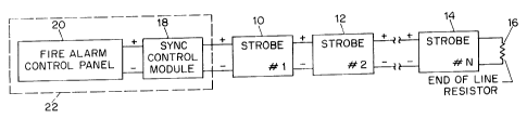
Referring to Fig. 1, multiple strobe circuits 10,
12 and 14 numbered from 1 to N, connected in a common loop
and, having the usual end of line resistor 16, are all caused
to flash at the same time, in synchronism, by a sync control
circuit 18. The sync control module 18 may either be
incorporated in a conventional fire alarm control panel 20,
as indicated by the dotted line enclosure 22, or may be a
free-standing unit interposed between the control panel and
the first strobe circuit 10 of the loop. Sync control
-6-
29438-479/25259
~~~~Ubi
module 18 is energized from a D.C. power source embodied in
control panel 20 in the same way that loop-connected strobes
are usually energized in a supervised alarm system. During
supervision, when'the polarity of the power supply is
reversed from that indicated in Fig. 1, module 18 uses no
power (nor does it supply power to the strobes), but when an
alarm condition is present th~ palarity of the voltage is as
shown, which causes the control module to commence operation
in a sync mode, which includes supplying D.C, power to the
multiple strobes via a two-wire loop. The sync contral
module causes all of the strobes in the loop to cyclically
flash in synchronism by periodically interrupting the supply
of power to the strobes. Typically, the power is
interrupted for a period of from 10 to 30 milliseconds, at
intervals of 2.9 seconds, so as to cause all strobes to
flash once about every 3 seconds. This flash rate satisfies
the UL requirement of a minimum of on~ flash every three
seconds and a maximum of three per second. This
synchronizing signal, namely, the brief interruption in the
supply voltage, in addition to triggering firing of the
multiple strobes also resets the internal timer of each
strobe unit to ready it far arrival of the next sync signal,
and to enable it to self-fire in the event no synchronizing
signal arrives after an interval exceeding 2.9 seconds
following~the last previous flash.
As will later be explained in detail, sync control
circuit 18 is designed to synchronize flashing of multiple
loop-connected strobes of various deaiqns including, for
example, modifications of the optocoupler strobe circuit
described in U.S. Pat. No. 5,121,033 granted on June 9, 1992
CA 02132061 2002-07-15
29438-479/25259
to applicant Kosich, and of the microprocessor-controlled
strobe disclosed in applicants' U.S. patent 5,341.,069 of
23 August 1994 and assigned to the same
assignee as the present application. In order for the
present sync circuit to work with a particular one of these
strobe circuits, the strobe must be modified to include as a
minimum the features and properties embodied in the basic
strobe circuit depicted in Fig. 2, several of which may be
connected in the loop of the system 'shown in Fiq. 1. The
1o flash unit l0 includes a flashtube DS1 shunted by a trigger
circuit which includes a resistor R1 connected in series
with the combination of a timer trigger 32 connected in
parallel with the series combination of a capacitor C1 and
the primary winding of an autotransfonaer T1. The secondary
winding of the autotransformer is connected~to the trigger
band of the flashtube arid when timer trigger 32 is fired
capacitor C1 discharges through the autotransformer and
produces a high voltaqs trigger pulse which,. if the voltage
across the flashtub~, as determined by a capacitor C2
connected in parallel with the flashtuba, exceeds its
threshold firing voltage, causes the flashtube to conduct
r
and quickly discharge capacitor C2.
Capacitor C2 is incrementally charged from a
suitable D.C.-to-D.C. oscillator 34~ through an inductor L1
which is connected to the positive terminal of capacitor C2
through a resistor R2 connected in series with a diode D2.
The node between inductor L1 and resistor R2 is connected to
ground through a switch Q1, which may be a MOSFET. The
D.C.-to-D. C. oscillator 34 is connected across a D.C.
voltage source, represented by Vii, and includes means for
_g_
29438-479/25259
closing and opening switch Q1 for connecting and
disconnecting inductor L1 across the D.C. source. Energy is
stored in the inductor during closed periods of the switch
and this stored energy is transferred from the inductor to
capacitor C2 during open periods of the switch. The
repetitive opening and closing of switch Q1, which may cycle
at a frequency in the range from about 3,000 Hz to about
30,000 Hz, will eventually charge capacitor C2 to the firing
threshold voltage of the flashtube.'
Faced with the reality that the supply voltage to
strobe alarms, even through typically D.C., may vary between
wide limits, in order to meet UL specifications that the
flash rate of the strobe must meet minimum requirements for
the range of voltages far which the strobe is to operate,
strobe circuits have heretofore been designed to expend the
required energy for the lowest reasonably expected voltage.
As a consequence, aupply voltages greater than the lowest
reasonably expected value would unnecessarily expend energy
in the flash above the minimum, more often than needed
and/or. in a non-useful manner. For example, the capacitor
C2 connected across the flashtube charges faster for higher
input voltages; thus, if the flash is actuated when the
potential across the capacitor attains the threshold firing
voltage of the flashtube, the flash rate will increase,
resulting not only in a waste of energy but also unnecessary
wear and tear on the capacitor. In the case of the
flashtube being triggered by a separate timing circuit, such
as the timer trigger 32, a higher input voltage will cause
overcharging of the storage capacitor, or at least make it
necessary to provide a larger capacitor than should be
_g_
~.
29438-479/25259
necessary. As a result, the potential across the capacitor
will cause a brighter than necessary flash, thereby wasting
energy.
In order to minimize unnecessary expenditure of
energy, yet provide sufficient energy per flash at a
constant frequency to mast minimum standards, the strobe
circuit of Fig. 2 includes an energy limiter circuit which
adjusts the amount of energy transferred to capacitor C2
responsively to changes in amplitude of the supply voltage.
The energy limiter may take the farm of a voltage regulator
36 connected in series with D.C.-to- D.C. oscillator 34
across the voltage source. Alternatively, it may be a
voltage regulator 36~ connected between oscillator 34 and
the positive terminal of capacitor C3, or a voltage
regulator 36~' connected from the junction of inductor L1 and
resistor R2 to the negative side of the voltage source.
In order that the strob~ circuit of Fig. 2 b~
triggered by sync control module 18, a positive potential is
normally supplied to a sync trigger circuit 38 via a
conductor 40 connected to the positive terminal of the
;t voltage source (which, it will be seen is a positive output
terminal of sync control module 18). This potential also
normally powers the internal timer trigger 32. Each time
sync control module 18 briefly interrupts this voltag~,
timer trigg~r 34 is disabled and sync trigger 38 is enabled
and triggers the firing of the flash unit.
The preferred embodiment of the sync control
cixcuit 18 shown in Fig. 3 is connected across a D.C.
voltage source which supplies a voltage Vin. The supply
voltage Vin may have a wide range of values, from 20 volts
-10-
29438-479/25259
~1~~~~i
to 31 volts, for example, in a nominally 24 volt system.
The voltage is normally applied through a double pole double
throw relay K1, shown in its normal position, to a pair of
output terminals which supply a voltage Vout to the input
terminals of strobe units 10, 12,... . ... N connected in
the loop. That is to say, except when it is operating in a
sync mode, the sync control circuit simply provides a direct
connection from a D.C. voltage source, typically housed in
the fire alarm control panel 20, to the loop connected
strobes, so as to enable each of them to operate
independently of the others at a flash rate determined by
its internal timer. '
The supply voltage Vin is also applied through a
diode D1, which typically has a voltage drop of 0.7 volt; to
a regulator circuit which includes resistors R4, R5, R6 and
R7, a transistor switch Ql and an integrated circuit U1
connected as Shawn and having component values so as to
provide a regulated 5.00 t 1% volt supply to the V~~ input
of a microcontroller U2. One terminal of resistor R4 is
connected to the cathode of diode D1 and at the other
,.r terminal is connected to both resistor R5 and the collector
of a switch Q1, which in this case is a transistor. The
other terminal of resistor R5 is connected to the base
electrode of switch Q1 and to an integrated circuit U1,
which acts as a controlled Zener for providing a precise
5.00 volts supply. Resistor R7 is connected between the
emitter of switch Q1 and the control pin of integrated
circuit U1. Resistor R6 is connected at one end to both
resistor R6 and the control pin of integrated circuit U1 and
at the other end to one end of U1, which is connected to the
-11-
29438-479/25259
~mz~b
negative side of the voltage source. Resistors R6 and R7
are of equal value for biasing integrated circuit U1. A
reset circuit for microcontroller U2 includes a diode D3, a
resistor~Ri and a capacitor C3. Diode D3 and resistor R1
are connected to each other in parallel, the cathode of
diode D3 being connected to the emitter of switch Q1 and its
anode being connected to both the positive terminal of a
capacitor C3 and the "CLEAR" input to microcontroller U2.
The other terminal of capacitor C3 is connected to the
negative side of the voltage source.
As noted earlier, a regulated potential of !5.00
volts is applied at vac of microcontroller U2; its V8s
terminal is connected to the negative, side of the voltage
source. A capacitor C4, connected across V~~ and Vo, acts as
a filter. A resonator circuit 9~~ consisting of an
oscillator Yi and capacitors Ci and C2 is connected across
the two oscillator inputs of, and supplies 4 l~iz
oscillations to, microcontroller U2. Capacitors C1 and C2
are respectively connected between the first and second
oscillator inputs of the microcontroller and the negative
',~ side of the voltage source.
Before describing the function of the
microcontroller U2, the components of the circuit affected
thereby will be described. Connected across vii is a branch
consisting of a diode D2, having a voltage drop of
approximately 0.7 volt, a switch Q3, in this embodiment a
Darlington transistor pair, the cail o! relay K1 and a
switch Q2, which in this embodiment is a MOSFET. The
voltage applied to the base electrode of one transistor of
the Darlington pair is regulated by a resistor R8 and a
-12-
29438-479/25259
2ener diode D~6 series-connected in that order between the
cathode of diode D2 and the end of the coil of relay K1 that
is connected to.switch Q2.
'Switch Q2 is cycled between a conducting state and
a nonconducting state by an output of microcontroller U2
which is applied to the gate of switch Q2 via a voltag~a
divider including a resistor R2 connected from the output
(Pin 9) of microcontroller U2 to the gate, and a resistor R3
connected from the gate electrode t~ the negative side of
the power source. When switch Q2 is closed, the pot~n~tial
at the output emitter of switch Q3 is pulled to that of the
negative side of the source, causing switch Q3 to conduct
and thereby cause current to flow through the coil of relay
K1 and switch the relay fram its normal position to the
other set of contacts. Actutaion of the relay reverses the
polarity of Vout, which amounts to interrupting the positive
D.C, voltage normally supplied to the controlled strobe
units. When switch Q2 is opened, switch Q3 stops
conducting, the relay is dean~rgized .and Vout is returned to
its original polarity. By controlling the opening and
closing of switch Q2, the rate at which the voltage supplied
to the strobes is interrupted, and for how long, is
regulated.
The real time clock and prascaler of
microcontroller U2, which in this embodiment is a PIC16C71
microcontroller having 8-bit resolution, are used to produce
signals for accurately controlling th~ ON time of switch Q2.
Typically, the real time clock and prescaler routine produce
pulses at Pin 9 which cause switch Q2 to be ON, and
therefore interrupt power to the strobes, for a period of
-13-
29438-479/25259
from 10 to 30 milliseconds, and to be OFF or open for 2.9
seconds. As illustrated by the simplified flow chart of
Fig. 4, upon initialization by the main microcontroller
program, switch Q2 is open and relay K1 is in the condition
shown in Fig. 3. Following a delay of 2.9 seconds, the
desired flash cycle of the controlled strobes, switch Q2 is
closed and switch Q3 conducts and energizes relay K1 for a
period of 10 to 30 milliseconds, following which the relay
is again turned off and the process~'is repeated. If for any
reason microcontroller v2 should fail to deliver a pulse to
switch Q2 2.9 seconds later, the relay will remain OFF and
D.C. power will be supplied to the individual controlled
strobes, allowing each to operate independently under
control of its internal timing trigger.
By way of example, the circuit shown in Fig. 3,
when energized from a 24 volt DC power source, may use the
following parameters to obtain the desired switching cycle:
E vALVE oR No.
..
.~
c1, ca cAP., 33pF, 20ov .
C3 CAP. , . 47~uF
,.c C4 CAP. , l5~tF, 16V
Dl, D2 DIODE, 1N4007
D3 DIODE, 1N914
D4 DIODE, 1N4742A
Q1 TRANSISTOR, 2N5550
Q2 TRANSISTOR, IRF710
Q3 TRANSISTOR TIP122
Rl RES., 39K, 1/4W, 5%
R2 ~ RES., 220, 1/4W, 5%
R3 RES., 100K, 1/4W, 5%
R4 RES., 330, 1/4W, 5%
R5 RES., 4.7K, 1/4W, 5%
-14-
29438--479/25259
~I~i~~bl
R6, R7 RES., 10K, 1/4W, 1%
R8 RES., 4.7, 1/ZW, 5% 4.7K
Ul I.C., TL431A
K1 RELAY, DPDT
U2 I.C., PIC16C54
Y1 CERAMIC RES., 4MHZ
As discussed earlier, sync control circuit 18
(Fig. 3) is designed to synchronize flashing of strobes of
various designs, including an optocoupler strobe circuit of
the type described in U.S. Pat. No. 5,121,033, provided it
has the features depicted in Fig. 2. A currently preferred
modification of the patented optocoupler strobe, shown in
Fig. 5, differs from the patented circuit in the respects
that it includes means for limiting the energy expended; a
sync trigger circuit; and, a rs-settabls internal trigger to
enable it to self-fire in the event the sync control circuit
fails to deliver a sync pulse at the appropriate time. A
storage capacitor C1 connected in parallel with the
flashtube is incrementally charged fxom an inductor L1 which
is connected to the positive terminal of the capacitor
through a resistor R3 connected in series with a diode D2.
The rate at which increments of energy are transferred from
inductor L1 to capacitor C1 is determined by an optocoupler
circuit which includes a resistor R2 connactsd in series
with inductor L1. When a switch Q1 is closed and connects
the inductor across the D.C, voltage source, Vin, the
voltage developed across resistor R2 is indicative of the
magnitude of the current flowing through inductor L1.
Opening of switch Q1 is controlled by an optocoupler U1
consisting of a light-emitting diode optically coupled to a
-15-
29438-479/25259
phototransistor detector. The voltage at the collector
electrode of the transistor portion of the optocoupler, arid
at the base electrode of switch Q1, is established by a
voltage divider consisting of a resistor R8 and a Zener
diode Z2 connected in series across the D.C. supply, a
capacitor C4 connected in parallel with diode Z2 and a
resistor R1 connected from the junction of resistor R8 and
diode Z2 to the aforesaid transistor collector electrode and
to the base electrode of switch Q1.~~ The diode Z2 protects
switch Q1 against over- voltage and provides the regulated
voltage required for the timing circuit. The capacitor C4
filters the regulated voltage, and is particularly needed
when the D.C. source is a full-wave rectified supply.
As pawer is initially supplied to the circuit
(that is, during the 2.9 seconds periods between sync
signals from the sync control circuit) the LED and
transistor of optocoupler U1 are both "off" and switch Q1
quickly turns "on" and connects inductor L1 across the D.C.
source. Closing of switch Q1 initiates charging of the
2o inductor L1 and a buildup of current through an isolating
diode D1 and resistor R2. When the current flowing through
inductor L1 attains a value sufficient to develop a voltage
across resistor R2 of approximately 1.2 volts, the
conduction threshold voltage of the LED portion of the
optocoupler, the diode is turned "on" and illuminates the
transistor portion to turn it "on" which, in turn, causes
switch Q1 to ba turned "off", thereby to diaconnsct inductor
L1 from across the D.C, source. During the open "off"
period of switch Q1, energy stored in inductor L1 is
transferred through resistor R3 and diode D2 to capacitor
-16-
29438-479/25259
~~~~~~1
C1. Upon cessation of current flow through resistor R2 due
to opening of switch Q1, the voltage drop across resistor R2
is no longer sufficient to keep the LED '°on", the transistor
stops conducting, switch Q1 is again turned "on" and the
cycle is repeated.
The "on" and "off" periods of switch Q1 are
determined by the switching characteristics of optocoupler
U1, the values of resistors R1, R2, R8 and Zener diode 22,
the values of inductor Ll and the vdltage of the D.C.
source, and may be designed to cycle at a frequency in the
range from about 3000 Hz to about 30,000 Hz. The repetitive
opening and closing of switch Q1 eventually charges
capacitor C1 to the point at which the voltage across it
attains a threshold value required to fire the flashtube.
Overcharging of capacitor C1 by a higher than designed
source voltage is prevented by a resistor R5 and a Zenar
diode Z1 connected in aeries between the base electrode of
the optocouplsr transistor and the positive electrode of
storage capacitor 12. The values of these components are
2o chosen so that when the voltage across capacitor C1 attains
the firing threshold voltage of the flashcube, a positive
potential is applied to the bass electrode of the
optocoupler transistor and turns "on" the transistor which,
in turn, turns switch Q1 "off" and disconnects inductor L1
from across the D.C. source.
The timer trigger circuit of the flash unit
includes a resistor R4 connected in series with the
combination of a switch Q3, which is this embodiment is an
SCR, connected in parallel with the series combination of a
3o capacitor C2 and the primary winding of an autotransformer
-17-
29438-479/25259
~;l~~~b ~
T1, the secondary winding of which is connected to the
trigger band of the flashtube. When the voltage across the
flashtubs exceeds its threshold firing voltage, switch Q3
conducts and the charge on capacitor C2 Plows through the
primary of transformer T1, inducing a high voltage pulse in
its secondary and causing the flashtube to conduct. As
previously mentioned, the flashtube quickly discharges the
energy stored in capacitor C1, readying it to be recharged
from the inductor L1 through diode D2.
The strobe circuit of Fig. 5 is triggered by the
sync control module 18, to the exclusion of the just-
described timer trigger, by a sync trigger circuit which
includes a resistor R~ and a capacitor C3 connected in
series in that order between the junction of resistor R8 and
diode Z2 and the negative side of the power source. A
switch Q2, which in this embodiment is a programmable
unijunction transistor, is connected in series with a
resistor R6 across capacitor C3, and a voltage divider
consisting of :arias-connected resistors R9 and R10 is
connected in parallel with the series combination of
resistor R7 and capacitor C3. The junction of resistors R9
and RlO,is connected to the gate electrode of the PUT, and
the positive terminal of resistor R6 is connected to the
gate electrode of the SCR Q3.
When tha regulated voltage supplied to the sync
trigger circuit is interrupted by~operation of sync control
module 18, the previously charged capacitor C3 discharges
through resistor R7, and when the voltage on capacitor C3
reaches a predetermined level as determined by the
characteristics of switch Q2 and the resistance values of
-18-
29438-479/25259
~1~~U~i
resistors R9 and R10, switch Q2 is turned "on" which, in
turn, turns SCR Q3 "on" to fire the flashcube. Shortly
after the flashcube fires, the short interruption period of
the applied potential terminates, and a positive potential
is again applied to diode D1 thereby to ready the circuit
for arrival of the next sync pulse. In this embodiment,
resistors R9 and R10 are external to switch Q2, enabling
better tolerance control over their values than when these
resistors are internal to switch Q2~as is the case in the
modified circuit shown in Fig. 6, which in all other
respects is identical to the circuit of Fig. 5. In the Fig.
6 switch Q2 is not a PUT but, instead, is a unijunction
transistor having two internal resistors corresponding to
resistors R9 and R10. Thus, the modification shown in Fig.
I5 6 has two fewer parts then the Fig. 5 circuit, at the
possible expense of less tolerance control.
Hy way of example, the circuit illustrated in Fig.
5, and the modification thereof shown in Fig. s, when
energized from a 24 volt D.C. power source, may use the
2o following parameters for the circuit elements:
~~.
ELEMENTS VALUE OR NO.
~r~
~o~~~~
C1 GAp., 47NF, 250V
C2 CAP., .047~tF, 400V
C3 CAP., 15~F, 5%
25 C4 CAP. , lS~tF, 5%
Dl DIODE, 1N4007
D2 DIODE, HER106
Ll INDUCTOR, 8.5mH
Zl DIODE, 240V.
30 Z2 DIODE, 9.1V., 5%
-19-
29438-479/25259
~l~i~~f~~
Ql TRANSISTOR, TRF710
Q2 PUT 2N6027 (Fig. 5); UJT
2N2646 (Fig. 6)
Tl TRIGGER TRANSFORMER
DSl FLASHTUBE
Q3 SCR, EC103D
R1 RES., 22K, 1/4W
R2 RES., 16.9
R3 RES, 180, 1/2W
R4 RES., 220K
R5 RES., 33K
R6 RES., 47
R' RES., 220K
R8 RES., 4.7X
R9, R10 RES. , lOIC, 1%
Ul OPTOCOUPLER, 4N3?
Fig. 7 is a circuit diagram of another strobe
circuit utilizing an optocouplar for D.G.-to-D. C. conversion
in which a combination of a CMOS timer and an SCR is used to
control firing and triggering of the flashtube in both the
synchronous and non-synchronous modes of operation..
Briefly, a capacitor C6 connected in parallel with the
flashtube is incrementally charged through a diode DS and a
resistor R11 from an inductor L1, which is cyclically
connected and disconnected across a D.C. supply by a switch
Q3 cantrolled by an optocoupler U2. A Zsner diode D2 and a
resistor R9 series-connected between the base electrode of
the transistor of the optocoupler and the po:itive terminal
of capacitor C6 shuts off the D.C./D.C, oscillator when the
capacitor is charged to maximum capacity, thereby limiting
the energy supplied to the flashtube~ to only what is
necessary. The trigger circuit for the flashtube includes a
-20-
29438-479/25259
~;3.~~U~~.
resistor Ri0 connected in series with the combination of a
switch Q2, which in this embodiment is an SCR, connected in
parallel with the series combination of a capacitor C1 and
the primary winding of an autotransformer T1, the secondary
of which is connected to the trigger band of the flashtube.
when switch Q2 is turned "on", in a manner to bs described
presently, capacitor C1 discharges through the primary of
transformer T1 and induces~a high voltage in the secondary
winding which, if the voltage on capacitor CG equals the
threshold firing voltage of the tube, causes the flashcube
to conduct and quickly discharge capacitor C6.
In this embodiment, switch Q2 is turned "on" in
both the synchronous and self-timed modes of operation by an
integrated circuit timer U1 which, in this embodiment is a
KS555 timer. The KS555 is a stable timer capable of
producing accurate time delays or frequencies, which for
stable operation as an oscillator, as here used, the free-
running frequency and the duty cycle are both accurately
controlled by two resistors R3 and R2 and a capacitor C3
connected in series in that order between the junction of a
resistor R6 connected in series with a Zensr diode D3 and
the negative side of the D.C. supply. The Zsnsr D3
regulates the voltage applied to the V~~ terminal of the
timer and to the junction between resistors R6 and R3. The
~~THRES" and "TRIG" terminals of the timer are connected to
the junctian between resistor R2 and capacitor C3 and the
DISCHARGE terminal is connected to the junction of resistors
R3 and R2. The RESET terminal is connected to the junction
between a resistor R7 and a capacitor C5 connected in series
across the D.C. supply, and the OUTPUT terminal is connected
-21-
~~J~i~b~
29438-479/25259
to the base electrode of a switch Q1, which in this
embodiment is a transistor. The junction between resistor
R7 and capacitor C5 is also connected via a diode D4 to the
terminal.
In this embodiment, resistors R2 and R3 have
resistance values of 100 ohms and 150K ohms, respectively,
and capacitor C3 has a value of 15~F. When operating in the
non-synchronous (i.e., self-timed) mode, capacitor C3 is
charged through resisters R3 and R2'until it has charged to
2/3V of the Zener voltage of diode D3. During charging, the
"OUT" Pin 3 of the timer is high, causing transistor Q1 to
conduct which, in turn, by reason of a connection from its
collector electrode to the gate electrode of SCR Q2, turns
the latter "Off". Once capacitor G3 has charged to 2/3V,
the voltage at Pin 7 causes Pin 3 to go low, which initiates
a discharge cycle. Capacitor C3 discharges through resistor
R2 only until its voltage reaches 1/3 of the voltage on D3,
which becsuse of the small resistance of R2 occurs in a very
brief time period. During this brief period, switch Ql is
turned "off" and applies a pulse to switch Q2 to turn it
,.~ "on", and the flashtube is fired. The timer provides
greater control over the flash rate in the non-synchronous
mode than does the circuit shown in Figs. 5, potentially at
less than 3 seconds intervals.
When operating in the synchronous mod~, the timer
U2 is in its charging or "on" state; when a sync pulse
arrives the D.C. power is interrupted by Pin 4 (RESET) of
the timer being pulled to ground through the action of the
series-connected resistor R7 and capacitor C5, the potential
at the junction of which is coupled to Pin 4 (RESET) and
-22-
29438-479/25259
also through diode D4 to the V~~ terminal of the timer.
Grounding of Pin 4 resets the timer, turning switch Q1 "off"
which, in turn, turns switch Q2 "on" to fire the flashtube.
Upon termination of the sync signal, which it will be
recalled has a period in the rmnge from 10 to 30
milliseconds, capacitor C3 is again charged through
resistors R6, R3 and R2 to ready the timer for arrival of
the next sync signal. ~In case a sync signal does not arrive
2.9 seconds later the timer will automatically go into the
described non-synchronous aelf-timed mode.
By way of example, the following parameters may be
used far the components of the Fig. 7 circuit, having a Vin
of 24V D.C., to obtain the indicated flash frequencies:
.
ELEMENT VALUE OR NO.
Gl CAP., 0.047~uF, 400V
C2, C3 CAP., 15~F, 16V
C4 CAP., O.Ol~F
C5 CAP. , 0. l~tF
C6 CAP. , 47~tF, 250v
D1 DIODE, 1N4007
D2 ZENER DIODE, 240V
D3 ZENER DIODE, 1N5239
D4 DIODE, 1N914
D5. DIODE, HER106
Ql TRANSISTOR, 2N4401
Q2 SCR, ?
Q3 TRANSISTOR, IRF910
Ll INDUCTOR, 8.?mH
R1 RES., 22k
R2 RES., 100
R3 RES., 150K
-23-
' 29438-479/25259
~~e~~~~.~
R4, R5 RES., lOK
R6 RES., 4.7K
R7 RES., lOK
R8 RES., 16.9
R9 RES., 33K
R10 RES., 220K, 1/2W
R11 RES., 180, 1/2W
U1 TIMER, KS555
U2 OPTOCOUPLER, 4I~135
Fig. 8 is a circuit diagram of a microcontroller
strobe circuit similar to that disclosed and claimed in
applicants copending application Serial No. 08/061,965
filed May 14, 1993, the flashing of which also may be
synchronized by the sync control circuit 18 of Fig. 3. The
circuit is connected across the D.C. voltage source,
supplied via the sync control circuit 18 as previously
described, having a voltage Vin. The voltaga is applied
through a diode Di, which typically has a voltage drop o!
0.7 volt, to a regulator which includes resistors R10, R11,
R12 and Ri3, a switch Q2 and an integrated circuit U1 for
providing a regulated 5.00 t i~ volts input to the Vac
terminal of a microcontroller U2. A precise V~~ input
voltage is vital for the analog-to-digital reference input
of mfcrocontrollar U2. Resistors R10 and Rii era connected
in series between the cathode of diode Di and the base
electrode of switch Qi, which in this case is a transistor,
and also to the cathode of integrated circuit Ui, which acts
as a controlled 2ener for providing 5.00 volts t 1~.
Resistors R12 and R13 are connected in aeries between the
emitter of transistor Q2 and the negative side of the
-24-
29438-479/25259
~ ~ i~ ~1.~
voltage source, and their junction is connected to the
control electrode of integrated circuit U1. Resistors R12
and R13 are of equal value for biasing integrated circuit
U1.
A reset circuit includes a diode D4, and a
capacitor C5 connected in series between the emitter
electrode of switch Q2 and the negative side of the D.C.
source, and a resistor R3 connected in parallel with diode
D4. The junction between diode D4 end capacitor C5 i:3
connected to the "CLRAR" terminal of microcontroller 1;J2. As
stated above, microcontroller U2 is supplied with a
regulated 5 volt supply at VAC; the Va, terminal is
connected to the negative side of the source. A capacitor
C8 connected across V~~ and V~~ acts as a filter. A
resistor R7 connected between one of the analog-to-digital
input terminals (PAO, Pin 17) of microcontroller U2 and the
negative side of the source acts as a shield for the
controller. oscillations at a frequency of 4MIiz are
applied to terminals OSC1 and OSC2 oig the microcontroller by
2o a resonator circuit consisting of an oscillator Yi.and a
pair of capacitors C1 and C2 connected between the negative
side of the source and the first and second oscilltor
inputs, respectively.
A voltage level proportional to the supply
voltage, Vin, is supplied to a different analog-to-digital
input terminal of the microcontroller, for example, the PA1
terminal (Pin 18). by a voltage divider network consisting of
a potentiometer R15, a resistor R9 and a resistor R4
connected in series between the junction of diode D1 and
resistor R10 and the negative side of the D.C. source, and a
_25-
- . ~I~~ilfi~
29438-479/25259
capacitor C6 connected in parallel with resistor R4. The
voltage developed at the junction between resistors R9 and
R4, which may be fine-tuned by the potentiometer R15, is
applied to the PA1 terminal.
The microcontroller U2 controls the opening and
closing of a switch Q1, which in this embodiment is a
MOSFET, by coupling a signal developed at an output terminal
P83 (Pin 9) via a voltage divider consisting of resistors R6
and R8 to the gate electrode of switch Q1. Switch Q1 is
connected in series with an inductor L1 and a diode D2, and
when closed connects the inductor across the voltage source,
Vin~ With switch Q1 closed, inductor L1 stores energy until
a steady state level is reached, or the switch is opened.
When switch Q1 is opened, the energy stored in inductor~Ll
is at least partially transferred through a diode D3 and a
resistor R14 to a storage capacitor G7 connected in parallel
with a flashtuba. 8y controlling the opening and closing of
switch Q1, the rats at which energy is stored in inductor L1
is regulated, thereby regulating the energy transferred to
2o storage capacitor C7. Diode D3 permits current flow into
the flash unit but prevents discharge of capacitor C7 when
the potential across it is higher than Vin or the potential
across inductor L1. The flashtubs is shunted by a trigger
circuit which includes a resistor R1 connected in series
with the combination of a switch Q3, which in this
embodiment is an SCR, connected in parallel with the series
combination of a capacitor C3 and the primary winding of an
autotransformer, the secondary winding of which is connected
to the trigger band of the flashtube. When, at the
appropriate time, a signal produced at the PA2 output of
-26-
~~ 29438-479/25259
microcontroller U2 is applied via a resistor R5 to the gate
of the SCR (Q3j, the SCR is fired and causes capacitor C3 to
discharge through the primary winding of the transformer,
inducing a high voltage pulse in the secondary winding which
ionizes the gas in the flashcube and causes it to flash,
provided the voltage thereacross equals or exceeds the
threshold firing voltage. A resistor R2 connected between
the gate electrode of the SCR and the negative side of the
~.C. supply isolates the SCR from nbise.
1n Microcontroller U2, which in this embodiment is a
PIC16C71 microcontroller having a built-in analog-to-digital
converter with 8-bit resolution, uses the A/D canverter to
arrive at a digital equivalent of the, supply voltage and
then uses this digitized information to control the opening
and closing of switch Q1, and thus the charging of inductor
L1 and the transfer of energy from the inductor to capacitor
C7, so that the output PA2 triggers switch Q3 to fire the
flashtube at the same time that the potential across the
capacitor C7 has attained the desired value. More
particularly, the A/O converter measures the supply voltage
in 256 steps of approximately 1/4 volt each. The
microcontroller program U2 equates each step with a location
in a look up table. One conversion or measurement is made
for each cycle of the switch Q1, a new value being read from
the lookug table each time. These values control the ON
time of switch Q2. The ON time for each value in the lookup
table is empirically derived; for low voltages, the ON time
is long, and for high voltages, the ON time is shorter,
whereby the energy stored throughout a flash cycle is kept
somewhat constant.
_27_
29438-479J25259
The switching frequency of switch Q1 is in the
range of approximately 3 kHz to 30 kHz and has a high duty
cycle (roughly 50% to 90%). Hach value in the lookup table
equates to a switching frequency for ensuring that switch Q2
will be ON for sufficient time to charge capacitor C7 to the
precise amount needed for the minimum required intensity of
once per three seconds flash, for example. The high duty
cycle results in storing of the energy in inductor L1 for
most of the three seconds interval between flashes. ~rhis
l0 means that peak currents are lower than if the routina~
utilized a low duty cycle in which inductor L1 was charged
for a relatively shorter period during each flash cycle.
If the supply voltage sensed is below a minimum
(e. g., less than 13 volts, below which it may be impossible
to obtain the precise 5.00 volts ~ i%) microcontroller U2
turns switch Q1 OFF and waits for the level to rise above
the preset start up voltage (e. g., 14 volts).
Microcontroller U2 has an interrupt, a real time
clock and a prescaler which are used to produce an accurate,
one per three seconds flash rate. The real time clock and
prescaler generate a one~fifteenth of a second interrupt.
The interrupt service routine then counts these pulses.
When fifteen pulses have occurred, a pulse is sent to the
~CR.Q3 and the flashtube is triggered. The interrupt
routine additionally controls the variabl~ OFF time
function. The OFF time of switch Q1 is programmed to be a
different pr~determinad value dependant on the number of
cycles completed in the fifteen hertz rate of the interrupt
(i.e., dependent on the time since the last flash). A high
value of OFF time is used after a trigger event, followed by
-28-
29438-479/25259
~1~~~~ii
several progressively lower values. This helps to minimize
current anamalies during and immediately after a flash.
By way of example, the following parameters may be
used for the elements of the Fig. 8 circuit to abtain a
flash frequency of oue flash per three seconds:
.~~..~~..
ELEMENT VALUE OR NO.
C1, C2 CAP., 33pF, 200V
C3 CAP. , . 047~tF, 400V
C5 CAP. , . 4'~~tF
CCa CAP. , . l~tF
CAP., 150~F, 250V.
CS CAP. , lS~tF, 16V
Dl, D2 DIODE, 1N4007
D3 DIODE NER106
D4 DIODE 1N914
L1 IN
DiJCTOR, 8.7 mH
Q1 _
TRANSISTOR, IRF740
Q2 TRANSISTOR, 2N5550
~3 SCR, EC103D
R1 RES., 220K
R2 RES., lOK
R3 RES., 39K
R4, R5 RES. 1K
Rs ~ RES., 220
R7 ~ RES., 100
RS RES., 100K
Ran RES., 11.3K
R10 RES., 330
R11 RES., 4.7K
R12, R13 RES., IOK
R14 RES., 120
R15 . POT., 1K
T1 TRANSFORMER, TRIGGER
U1 I.C., TL431A
-29-
29438-479/25259
U2 I.C., PIC16C71
Y1 CERAMIC RES., 4MHz
While up to this point the invention has been
described in association with a fire alarm system including
a fire alarm control panel which controls multiple strobes
connected in a single loop, conventional fire alarm control
panels may, and often do, control more than one loop of
multiple strobes. The several loopm may, for example, be
installed in different zones or sections of a building,' in
which case it would not be necessary to synchronize flashing
of the strobes in all of the loops, but in other situations
it may be desirable to synchronize flashing in one or more
of loops presenting an alarm condition. The control unit
illustrated in Fig. 3 could not by itself perform these
functions, yet in the interest of cost it is desirable to
avoid having to provide a separate controller for each of
the loops. The control circuit shown in Figs. 9 and 10
enables one microcontroller to control up to four separate
loops or zones, and may be expanded to control ona~or more
additional controllers each capable of controlling an
additional four loops of strobes. Referring to Figs. 9 and
10, in which components common to Fig. 3 are correspondingly
identified, a single microcontroller U2, which may be a
PIC16C54, is capable of controlling up to four loops of
strobes (not shown) which are connected to the positive and
negative OUTPUT terminals of four relay circuits labeled
ZONE 1, ZONE 2, ZONE 3 and ZONE 4, respectively. When and
only when an alarm condition is present in a zone, a D.C.
voltage, typically 24 volts, is applied across its positive
-30-
29438-479/25259
and negative INPUT terminals, and a relay K connected to the
positive terminal when in the condition shown in Fig. 9,
supplies this voltage to the strobes connected in a loop to
that zone. As will be described presently, the
microcontroller U2 produces signals at its output pins 6, 7,
8 and 9 which are applied to control circuitry in ZONES 1,
2, 3 and 4, respectively, which momentarily open a
corresponding relay K, for.a period of 10-30 milliseconds,
thereby interrupting power to and triggering flashing of the
strobes powered through that relay.
Referring in detail to Fig. 9 and the ZONE 1
circuitry, the positive side of the D.e, input voltage is
coupled through a diode D10 to a terminal labeled "V+" and a
negative side is coupled through a diode D12, the emitter-
collector path of a bipolar NPN transistor Q4 and a diode
D14 to a terminal labeled "V-"~ A potential exists between
these V+ and V- terminal only when a O.C. potential, Vin, is
applied to the ZONE 1 input terminals: The same is true of
th.e ZONE 2, ZONE 3 and ZONE 4 circuits, namely, that a
potential appears across their V+ and V- terminals when, and
,,~ only when, a D.C. potential indicating an alarm condition is
applied to their input terminals. The terminals labeled
"V+" in all four zones are actually internally connected
together and to a similarly labeled terminal of a power
regulator circuit (Fig. 10) and the terminals labeled "V-"
in all four zones are internally connected togother and to
the negative side of the power regulator circuit. Thus, a
potential is applied across the "V+" and "V-" terminals of
the power regulator only if one or more of the four zones is
energized.
-31-
29438-479/25259
~~~~~~x
To enable the microcontroller to determine which
of the four zones is energized, particularly when more than
one are energized at the same time, each is isolated from
the others by an isolation circuit including the
aforementioned diodes D10, D12, D14 and transistor Q4 and a
resistor R15 connected betwe~n the positive side of the D.C.
input voltage and the base electrode of transistor Q4.
Diode Dlo is a blocking diode which prevents current flow
from the commonly-connected °°V+" teirminals to other zones
and also prevents current from such common circuit fri'm
forward-biasing transistor Q~ when a.zone, say ZONE 1,, is
energized. Tha negative side of the input D.C. is coupled
via diode D12, transistor Q4 and another diode D16 onto a
respective ZONE INPUT line to a respective one of four
inputs to microcontroller U2 labeled PBO, PH1, PB2 and PH3,
respectively. Each of these ZONE INPUT lines is connected
via a respeativs resistor R to a regulated +x.00 volts
supply (to be described) and via a respective capacitor C to
the negative side of the supply.
Regulated voltages for operating the system era
supplied, by the POtdER REGULATORS shown in Fig. 10 when, and
only when, one or more of the zones are actuated so as to
provide a potential, typically 24 volts, between the
internally connected terminals labeled "V+" and "V-". A
valtaga of 5.0 volts t 1% is produced at an output terminal
labeled °°+SV" by a r~gulatar which includes a diode D1,
resistors R4 and R5 and an integrated circuit U1 which acts
as a controlled Zener, connected in series in that order
from the V+ terminal to the V- terminal of the supply, a
3o transistor Q1 having its base electrode connected to the
-32-
.' 29438-479/25259
r. ,
~I~~i~b~t
junction of resistor R5 and integrated circuit Ui, its
collector connected to the junction of resistors R4 and R5,
and its emitter connected through series-connected resistors
R7 and R6 to the V- terminal of the power supply. The
junction of resistors R6 and R7 is connected to the control
pin of integrated circuit U1. A regulated potential of 5.0
Volts produced at the emitter of transistor Q1 is filtered
by a capacitor C8, and~appliad via an internally connected
terminal, also labeled °°+5V", to the V~~ input of the
l0 microcontsoller. The V", input of the controller is
connected to the V- terminal of the power supply.
A regulator for producing a potential of 12 volts
required for operation of ZONE and EXPANSION relays includes
a resistor R8 and a Zener diode D4 connected in series
across the supply, and a Darlington transistor pair Q3
connected in parallel with resistor R8 and in series with a
filter capacitor C9. The regulated 12 volts produced at the
output emitter of the Darlington pair appears at a terminal
labeled °°+12V" which is internally connected to a similarly
labeled terminal in each of the ZONE circuits and also in
~ the EXPANSION circuit. It is again emphasized that the
controller is powered only when at least one ZONE is
energized.
The clock frequency of the microcontroller is
determined by a 4MHz resonator Y1 and a pair of capacitors
C1 and C2 connected to the OSC1 and OSCa terminals,
respectively, of the controller. When energized upon the
occurrence of an alarm condition in a ZONE, the
microcontroller is, programmed to monitor the ZONE INPUTS and
ascertain which of them is activated, and then toggles a
-33-
29438-479/25259
..
relay K in the circuitry for the corresponding ZONE for a
period in the range from 10 to 30 milliseconds, thereby
briefly interrupting the application flow of power to the
strobes associated with that ZONE.
More particularly, and assuming that the
microcontroller has sensed that ZONE 1 has been energized,
after a delay of 2.9 seconds following initial sensing of
the alarm condition, a +5.00 volts signal is produced at
output terminal PAO (Pin 17) and coupled via a respective
1o RELAY OUTPUT line to the gmte electrode of a MOSFET Q5 via a
voltage divider including resistors Ris nd R17 connected in
series and to the terminal "V-". The junction of resistors
R16 and R17 is connected to the gate electrode of Q5, the
source and drain electrodes of which are connected in series
with the coil of relay K across the power supply represented
by terminals "V+" and "V-". When switch Q5 is turned "ON"
by the signal from Pin 17, relay K is activated, thereby
interrupting power flow to the strobes For a short, hardly
noticeable, interval. An optional diode D18 connected
2o acrosa the relay coil suppresses the reverse EMF spike that
x is generated when switch Q5 is opened, but may be omitted in
the interest of increasing the switching speed of the relay.
If, for example, the controller also senses an
alarm condition in ZONE 4, a +5.00 volts signal is also
produced at output terminal PA3 (Pin 2) which turns "ON" the
MOSFET and actuates the relay K in the ZONE 4 circuit in
synchronism with actuation of the relay in the ZONE 1
circuit, Whereby the strobes in the loops associated with
both zones will be fired at the same time. Alternatively,
to preclude the creation of possible anomalies in current
-34-
m,..... , ....
-.,
29438-479/25259
flow that might result from all strobes in the four loops
flashing at the same time,.the microcontroller may be
programmed to interrupt the power in the four loops at
staggered times within the 2.9 seconds interval. That is to
say, the 2.9 seconds interval may be divided into four time
slots of approximately .75 second each in which triggering
of the four zones is initiated sequentially. The flashing
would be harmonious, if not synchronous, but would meat
underwriters Laboratories specifications for flash rates.
l0 In accordance with another aspect of the
invention, synchronized firing of the strobes in more than
four loops can be controlled by providing the controller
with an EXPANSION circuit having EXPANSION INPUT and
EXPANSION OUTPLtT terminals, as shown in the lower right-hand
portion of Fig. 10, which are connected in "daisy-chain"
fashion as depicted in Fig. 13, to the EXPANSION INPUT and
EXPANSION OUTPUT terminals of one or more similarly equipped
controller of the kind just described, each for controlling
four loops of flash units. More particularly, the expansion
output.terminals of a first controllsr, labeled "CONT. #1",
are connected to the expansion input terminals of a second
controller, CONT. f~2, the expansion output terminals of
which are connected to the expansion input terminals of a
thixd controller, and so on, with the expansion output
terminals of the last controller of the chain connected back
to the expansion input terminals of the first. Hv
connecting multiple controllers in this way, sync signals
generated by one controller in the chain as a consequence of
an alarm condition occurring in at least one of its
associated ZONES, may be transferred to the other
-35-
r' 1
29438-479/25259
~1~2~i~i.~
controllers in the chain. Because each of the
interconnected controllers is equally likely to experience
an alarm condition, and there is no way of knowing when, if
ever, a particular controller will be energized by
occurrence of an alarm condition, the EXPANSION circuit of
each controller must ba able to transfar sync signals from
the EXPANSION INPUT terminals to the EXPANSION OUTPUT
terminals whether the controller is powered or not.
To this end, the EXPANSION circuit includes a
relay K, the coil of which is connected between the "+5V"
and "V-" terminals of the microcontrollar and shunted by a
diode D20 for suppressing the back EMF spike created when
current through the coil is turned a~f. In the event of no
power on any of the four zones, with the consequence that
the microcontrollar U2 is not energized, the relay contacts
are in the illustrated non-energized position and
accordingly by-pass the controller. That is, contact 2 and
contactor 3 and contact 9 and contactor 8 respectively
directly connect positive and nagatiVa EXPANSION INPUT
terminals to positive and negative EXPANSION OUTPUT
terminals.
However, when an alarm condition occurs in at
least one ZONE to cause powering of the controller, currant
flows through the relay coil from the +5V bus to the
negative side of the supply and actuates the relay, whereby
a +12V potential is coupled through contact 4 and contractor
3 to the positive EXPANSION OUTPUT terminal and the drain
electrode of a MOSFET Q5 is coupled through contact 7 and
contactor 8 to the negative EXPANSION OUTPUT terminal, and
the positive and negative EXPANSION INPUT terminals are both
-36-
29438-479/25259
~l~Zt~b.~
disconnected. As a consequence the relay K no longer by-
passes the controller to transfer any sync signals generated
by another controller in the chain and appearing on the
EXPANSION INPUT line to the next successive controller. The
by-pass function is restored by a circuit including an
optocoupler U3, the light emitting diode of which is
connected in series with a resistor 22 across the EXPANSION
INPUT lines, and the transistor output portion of which is
connected in series with a rasistor~R23 between the ~~+5V"
and "V-" terminals of the POWER REGULATORS. The junction
between resistor R23 and the collector of the transistor is
connected to terminal P86 (Pin 12) of controller U2. If at
least one ZONE associated within another interconnected
controller is energized, there will be a 12 volt D.C.
potential across the EXPANSION INPUT lines, causing the
optocouplar diode to conduct and turn "on~~ the transistor
portion. Conduction of the transistor portion pulls the
potential on Pin 12 of the controller from +5V to zero,
which the controller is programmed to sense and cause
terminal Pe? (Pi~~ 13) to go "high". This voltage pulse is
applied to the gate electrode MOSFET Q6 via a voltage
divider.,including resistors R18 and R20, which turns Q6 ~~on"
and causes current flow in the diode portion of the opto-
coup.ler connected to the EXPANSION INPUT terminals of the
next controller in the chain. Thus, when the controller is
powered, the ~~axpanaion" sync signal is received through the
optocoupler and under control of the microcontroller is for-
warded via switch Q6 to the next controller.
Referring now to the flow chart of Fig. 12,
fallowing START the controller initially turns ~~off" all
-37-
29438-479/25259
~;~.~Z~l~i1
relays, that is, the relay in each of the ZONE circuits, and
also turns "OFF" the "expansion output pulse" to MOSFET Q6.
Following a short delay of about 1 second, a counter is
started which counts for about 2 seconds after which Pin 12
is read to determine whether it is at +5 volts, indicating
no expansion input, or zero in case there is an input. If
the answer is "No" the count of the counter is checked to
ascertain whether the ~ seconds has elapsed and, if not, pin
12 is again read. A °'Yes" decision'from either diamond
turns "ON" the expansion output pulse to MOSFET Q6 to pass a
signal on to the next controller. Than. the fear ~n~a
inputs (Pins 6, 7, 8 and 9) are scanned to determine which
is °°ON" or energized; it will be recalled that at least one
must be on, otherwise there will be no operating power for
the controller. When the "~N" 2ene nr ~n"oa beers bvwaw
identified, a relay output signal is applied to and turns on
the corresponding zone relays and thereby interrupt power to
the associated loop-cone~cted strobes for a short period, in
the range from 10 to 30 milliseconds, following which the
cycle is repeated.
As noted earlier, to preclude the creation of
possible anomalies in current flow that might result should
all of the strobes in all of the loops be flashing at the
same time, the microcontroller may be programmed to
interrupt the power supplied to the loops at staggered times
within the 2.9 seconds interval. R~f~rring to the
simplified flow chart of Fig. 14 which outlines the program,
following START the controller initializes parameters and
then turns "off" all relays, namely, the relay in each of
the ZONE circuits, and also turns "OFF" the "expansion
-38-
~. 29438-479/25259
~~~z~~~
output pulse" to switch Q6. Following a short delay of
about 60 milliseconds, a counter is started which counts for
about 3/4-second after which Pin 12 is read to determine
whether it is at 5 volts indicating no expansion pulse
input, or zero in case there is an input. If the answer is
''No" the count is checked to ascertain whether the 3/4-
second has elapsed and if not, Pin 12 is again read. A
"Yes" decision from either diamond turns on the expan~:ion
output pulse to switch q6 to pass a'sync signal to the: next
1~ controller. Then a first of the four zone inputs (e.g., Pin
6) is scanned to determine if it is "ON" and if energized, a
relay output signal is applied to and turns on that zone
relay and thereby interrupts power to the associated strobes
for a period in the range from la to 30 milliseconds. Next
the microcontroller repeats the process successively
scanning the remaining three zone inputs and applying relay
output signals to appropriate zone relays. The net result
is that the energized flash units in the four zones are
triggered sequentially at 3/4-second intervals within a
2~ period of about 3 seconds.
-39-