Note: Descriptions are shown in the official language in which they were submitted.
2 1 32 1 07
MULTIPLE RESONATOR OSCILLATOR CIRCUITS
Field of the Invention
This invention relates to multiple resonator
oscillator circuits.
Backaround of the Invention
A well known differential amplifier comprises a
matched pair of bipolar transistors, a matched pair of load
impedances and a current source. Each load impedance is
connected between a voltage supply and a collector of a
respective one of the transistors, and emitters of both
transistors are connected to the current source. A
differential input is applied to bases of the transistors,
and a differential output is taken from the collectors of
the transistors.
Two such differential amplifiers can be cross-
coupled to construct a quadrature phase Voltage Controlled
Oscillator (VCO) which oscillates with 90 degree phase shift
across each differential amplifier with 1~30 degree phase
shift in the cross-coupled feedback loop. Unfortunately,
the quality factors (Q) of such VCOs are smaller than
desired for many high frequency applications.
SummarY of the Invention
This invention provides multiple resonator
oscillator circuits having enhanced quality factors.
This invention provides a multiple resonator
oscillator circuit, comprising a plurality of two port
resonators. Each two port resonator comprises first and
second amplifiers and first and second ports. The first
amplifier has an input, an output, and a first gain and a 90
degree phase shift at a resonant frequency of the multiple
resonator oscillator circuit. The second amplifier has an
input coupled to said output of the first amplifier and an
,,~
2 2 1 32 1 07
Summarv of the Invention
This invention provides multiple resonator
oscillator circuits having enhanced quality factors. The
multiple resonator oscillator circuits, comprise a plurality
of two port resonators. Each two port resonator has a first
quality factor and comprises first and second amplifiers, and
first and second ports. The first amplifier has an input, an
output, and a first gain and a 90 degree phase shift at a
resonant frequency of the multiple resonator oscillator
circuit. The second amplifier has an input coupled to the
output of the first amplifier and an output cross-coupled to
the input of the first amplifier. The second amplifier has a
second gain and a 90 degree phase shift at the resonant
frequency of the multiple resonator oscillator circuit.
Consequently, each two port resonator has a loop gain defined
by a product of the first and second gains. The first port
is coupled to an input of one of the first and second
amplifiers and the second port is coupled to an output of
said one of the first and second amplifiers. Consequently,
the first and second amplifiers define a first port to second
port gain and a second port to first port gain for each two
port resonator. The first port to second port gain exceeds
the second to first port gain. The two port resonators are
connected in a ring to provide a ring gain defined by a
product of the first port to second port gains. The ring
gain dominates the loop gain and is greater than unity. The
connection of the two port resonators is such that the
multiple resonator oscillator circuit has a second quality
factor exceeding the first quality factor.
Brief Descri~tion of Accom~anYina Drawinqs
Embodiments of the invention are described below by
way of example only. Reference is made to accompanying
drawings, in which:
Figure lA is a circuit diagram of a novel
di~erential amplifier;
1~ 3 2132107
Figure lB illustrates a symbol used to denote the
differential amplifier of Figure lA;
Figure 2 is a schematic diagram of two differential
amplifiers as shown in Figures lA and lB, connected as a
~uadrature phase voltage controlled oscillator;
Figure 3A is a schematic diagram of two differential
amplifiers as shown in Figures lA and lB connected as a
differential two port bidirectional resonator;
Figure 3B illustrates a symbol used to denote the two
port resonator of Figure 3A;
Figure 4 is a schematic diagram of two resonators as
shown in Figures 3A and 3s connected as a band pass filter;
~J
WO93/19517 PCT/CA92/00~34
4 ~32107
Figure 5 is a schematic diagram of four resonators
as shown in Figures 3A and 3B connected in a ring as a four
resonator quadrature phase voltage controlled oscillator;
Figure 6A is a circuit diagram of a modified
differential amplifier used to construct embodiments of the
invention;
Figure 6B illustrates a symbol used to denote the
differential amplifier of Figure 6A;
Figure 7 is a schematic diagram of two
0 differential amplifiers as shown in Figures 6A and 6B
connected as a differential two port resonator having
unequal bidirectional gain, an embodiment of the invention;
and
Figure 8 is a circuit diagram of a peak detector
and bias control circuit for use in the two port resonator
of Figure 3A.
De~r;~t~ nn o f ~mho ~ ; m~n ts
Figure l is a circuit diagram of a differential
amplifier l00. The differential amplifier l00 has a
differential input in the form of input terminals Ip, In and
a differential output in the form of output terminals Op,
n . First and second matched load impedances l0, 12 (each
approximately l.5 kOhm) are connected between a 5 volt
2s positive supply 14 and the differential output terminals
p~ n respectively. A first pair of ma~ched bipolar
transistors 20, 22 has collectors connected to the
differential output terminals Op, n respectively, bases
connected to the differential input terminals In~ Ip
respectively and emitters connected to a common first node
24. Each of the first pair of transistors 20, 22 has an
emitter area approximately 0.8 microns by 4.0 microns. A
second pair of matched bipolar transistors 30, 32 has
collectors connected to the differential output terminals
35 p~ n respectively, bases connected to the differential
W093/19517 PCT/CA92tO0~34
1 3 2 1 0 7
input terminals In~ Ip respectively and emitters connected
to a common second node 34. Each of the second pair of
transistors 30, 32 has an emitter area approximately 0.8
microns by 20 microns. A current dividing circuit in the
form of a third pair of matched bipolar transistors 40, 42
has collectors connected to the first and second nodes 24,
34 respectively, bases connected to differential control
input terminals Cn, Cp respectively, and emitters connected
to a current source 50. The current source 50 is connected
to a 5 volt negative supply 52. A pair of matched
capacitors 60, 62 (each approximately O.l pF) is connected
between the positive differential input terminal Ip and the
negative differential output terminal n and between the
negative differential input terminal In and the positive
differential output terminal Op respectively.
In operation of the differential amplifier lOO,
the current source 50 supplies a substantially constant
bias current which is divided between first and seçond
20 current paths defined by the third pair of transistors 40,
42 respectively. A control voltage differential applied
between the control input terminals Cn, Cp controls the
division of the bias current between the first differential
pair 20, 22 and the second differential pair 30, 32. The
first differential pair 20, 22 and the second differential
pair 30, 32 each amplify a signal voltage differential
applied between the signal input terminals In~ Ip to provide
an amplified voltage differential between the signal output
terminals n~ Cp. Figure lB illustrates a symbol used to
30 denote the differential amplifier lOO.
Figure 2 is a schematic diagram of two
differential amplifiers lOO, lOO', connected as a resonant
circuit in the form of a quadrature phase Voltage
35 Controlled Oscillator (VCO) 200. The positive and negative
WO93/19517 PCT/CA92/00534
6 21 321 07 ~
output terminals Op, n of differential amplifier lO0 are
connected to the positive and negative input terminals Ip,
In respectively of differential amplifier lO0~, and the
positive and negative output terminals Op, n of
differential amplifier lO0' are connected to the negative
and positive input terminals In~ Ip respectively of
differential amplifier lO0. The control input terminals
Cn, Cp of the amplifiers lO0, lO0' are connected in parallel
to an adjustable control voltage source 210. The VCO
output is taken from the output terminals Op, n Of one of
the amplifiers lO0'.
The vCo 200 oscillates at a frequency where the
series gain of the amplifiers lO0, lO0' is greater than
unity and the total phase shift contributed by the
amplifiers lO0, lO0' is 180 degrees, a further 180 degree
phase shift resuLting from the cross-coupling of the
amplifiers lO0, lO0~. The amplifiers lO0, lO0~ are biased
identically, so each contributes a phase shift of 90
degrees at the oscillation frequency.
The oscillation frequency of the vCo 200 is tuned
by adjusting the differential voltage Vc applied between
the control inputs Cp, Cn of the differential amplifiers
lO0, lO0' so as to adjust the division of bias current
between the first differential pair 20, 22 and the second
differential pair 30, 32 of each amplifier lO0, lO0'. When
most of the bias current is steered to the smaller
differential pairs 20, 22, they have a larger differential
30 gain than the larger differential pairs 30, 32, and the
frequency response of the smaller transistors 20, 22
dominates the frequency response of the amplifiers lO0,
lO0~. Conversely, when most of the bias current is steered
to the larger differential pairs 30, 32, they have a larger
differential gain than the smaller differential pairs 20,
WO93/19517 PCT/CA92/00~34
7 2132107
22, and the frequency response of the larger transistors
30, 32 ~s~in~tes the fre~uency response of the amplifiers
100, 100'.
The frequency responses of the transistors 20, 22,
30, 32 are largely determined by their UMiller
capacitance~, i.e. the effective capacitive impedance of
the transistors between their base and collector terminals.
The Miller capacitance at a given frequency increases with
o the transistor gain at that frequency, and the transistor
gain increases with the emitter current density. When most
of the bias current is steered to the smaller transistors
20, 22, the emitter current density is relatively high, so
the transistor gain and Miller capacitance are relatively
high, and the 90 degree phase shift required for
oscillation occurs at a relatively low fre~uency.
Conversely, when most of the bias current is steered to the
larger transistors, the emitter current density is
relatively lower (because the same bias current is applied
to transistors having a larger cross-sectional area), so
the transistor gain and Miller capacitance are relatively
lower, and the 90 degree phase shift required for
oscillation occurs at a relatively higher frequency. The
base resistance of the smaller transistors 20, 22 is also
larger than the base resistance of the larger transistors
30, 32, and this further increases the difference in 90
degree phase shift frequencies for the two differential
pairs 20, 22, 30, 32. Consequently, the oscillation
frequency can be tuned between two extreme values by
controlling the division of bias current between the
smaller differential pair 20, 22 and the larger
differential pair 30, 32 in each of the amplifiers 100,
100~. The VCO 200 can be tuned from approximately 0.75 GHz
to approximately 1.4 GHz with a control bias voltage of
approximately 2 volts above ground and control voltage
differential from -0.075 volts to +0.075 volts. This
tuning range is more than adequate to compensate for
WO93/19517 PCT/CA92/00~34
8 2~2~
circuit parameter variations resulting from typical
manufacturing process variations.
In the VCO 200, the emitter areas of the smaller
5 differential pairs 20, 22 and the larger differential pairs
30, 32, the values of the load impedances lO, 12, and the
bias currents are selected so that the gain of each
differential amplifier lO0, lO0' is near unity over the
oscillation frequency range. The selected bias current may
vary somewhat according to the manufacturing process used,
but a total bias current of approximately 0.5 mA is typical
for the sicMos process in which the VCO 200 was
implemented. This restriction on the amplifier gains
ensures that the amplitude of oscillations does not force
the transistors 20, 22, 30, 32 to cut off so that each
amplifier lO0, lO0' operates in ~class A~ or linear mode.
Consequently, the filtering action of the Miller
capacitances and base resistances of the transistors 20,
22, 30, 32 is present throughout the oscillation cycle, and
the VCO 200 has a relatively high quality factor (Q). For
maximum Q, the loop gain (i.e. the product of the amplifier
gains) should be approximately l.05 (0.5 dB) at the 90
degree phase shift frequency, although a relatively high Q
can be achieved for loop gains up to approximately l.4 (3
dB).
The matched capacitors 60, 62 increase the Miller
capacitance of both differential pairs 20, 22, 30, 32 of
both amplifiers lO0, lO0'. The increased Miller
capacitance shifts the oscillation frequency range to a
lower frequency band. Moreover, by increasing the Miller
capacitance and lowering its dependence on nonlinear
operating parameters of the amplifier circuit, the matched
capacitors 60, 62 further increase the quality factor (Q)
of the VCO to between 15 and 50, significantly higher than
could be obtained without the capacitors 60, 62.
WO93/19S17 PCT/CA92/00534
-- 9 2 1 32 1 û7
Figure 3A is a schematic diagram of two
differential amplifiers 100, 100' connected as a resonant
circuit in the form of a differential two port
bidirectional resonator 300. The two port bidirectional
resonator 300 is essentially the same as the VC0 200 with
the addition of terminals Ap, An connected to the
differential outputs Op, n Of the amplifier 100 defining a
first port, and terminals Bp, Bn connected to the
differential outputs Op, 0~ of the amplifier 100' defining a
lo second port which is in quadrature phase with respecr. to
the first port at the resonant frequency. Figure 3B
illustrates a symbol used to denote the resonator 300.
The resonator 300 resonates at a frequency where
the phase shift across each amplifier 100, 100' is 90
degrees, so that tAe total phase shift around the loop is
360 degrees, a 180 degree phase shift resulting from the
cross-coupling of amplifier 100' to amplifier 100. If the
loop gain is greater than 1, the resonator 300 oscillates
20 at its resonant frequency. If the loop gain is less than
1, the resonator acts as a bandpass filter having a
passband centered on its resonant frequency.
Resonators 300 can be used to construct filters
and VCOs having higher quality factors (Q) than the VCO
200. Figure 4 is a block schematic diagram showing a
multiple resonator circuit in the form of two resonators
300, 300' connected in series via coupling capacitors 410
to construct a bandpass filter 400. The load impedances
10, 12 of each amplifier 100, 100' of each resonator 300,
300' are selected to ensure that each resonator 300, 300'
has a loop gain less than unity at the resonant frequency.
The coupling capacitance is selected in accordance with the
desired passband characteristics. According to known
characteristics of coupled resonators, the filter 400 will
have a passband which is flat at the resonant frequency of
WO93/19517 PCT/CA92/00~34
- lo 2 ~ 3~ 1 07
the individual resonators 300, 300~ if the resonators 300,
300' have equal loop gains and the coupling capacitance
equals (C1C2)l/2(QlQ2)~ , where Cl and C2 are the equivalent
capacitances at the ports of the resonators 300, 300', and
5 Q1 and Q2 are the quality factors of the resonators 300,
300'. If the coupling capacitance is less than (ClC2) 1/2
(QlQ2)-l~2, the filter 400 will have a quality factor (Q)
which is higher than either of Ql and Q2. Further series-
coupled resonators could be added to further enhance the
quality factor (Q) of the filter 400. (See F.E. Terman,Electronic and Radio Engineering, Fourth Edition, McGraw-
Hill, 1955, p. 67-73.)
Figure 5 is a block schematic diagram showing a
multiple resonator circuit in the form of four resonators
300 connected in a ring to construct a VCO 500. The load
impedances lO, 12 of each amplifier lO0, lO0~ of each
resonator 300 are selected to ensure that the ring gain of
the VCO is greater than unity at the resonant frequency.
The phase shift of each resonator 300 at the resonant
frequency is 90 degrees, so that the phase shift around the
ring is 360 degrees at resonance, satisfying the phase
conditions required for oscillation.
2s It can be shown that each resonator 300 of the VCO
500 acts as a transformer with a small step up ratio, so
the signal power of the individual resonators 300 adds
arithmetically around the ring. Conversely, the noise
power of the individual resonators 300 can be characterized
by independent Gaussian variables which add in RMS fashion
around the ring. Consequently, the quality factor (Q) of
the VCO 500, which is proportional to the signal power
divided by the noise power, should be higher than the
quality factor of the individual resonators 300 by a factor
of nl/~=2 (where n is the number of resonators 300 in the
ring) due to power considerations alone.
WO93/19517 PCT/CA92/00~34
2 1 3 2 1 0 7
There is a further increase in quality factor (Q)
due to the effect of the ring connection on the bandwidth
of the VCO 500. Each resonator 300 in the VCO 500 receives
feedback around the ring in addition to internal feedback
5 around its own loop. Because there are four phase shifting
amplifiers in the ring feedback path and only two phase
shifting amplifiers in the loop feedback path, the VCO 500
will have a narrower 3 dB bandwidth than the individual
resonators 300. The ring and loop feedback signals add
vectorially to determine the resonance characteristics of
the VCO 500. If the ring feedback dominates the loop
feedback, it can be shown that the ring connection further
enhances the quality factor (Q) of the VCO up to n2=l6
times (where n is the number of resonators in the ring), so
the total quality factor enhancement can be as high as
ns/2=32.
Unfortunately, in the VCO 500 the combined loop
gain of the resonators 300 making up the VCO 500 exceeds
the ring gain, so the loop feedback dominates the ring
feedback, and the resonance of each resonator 300 ~in~tes
the resonance of the ring. This limits the enhancement of
the quality factor (Q) that can be achieved by
concatenation of the resonators 300 to a factor of
approximately three. This limitation can be overcome by
modifying the design of the differential amplifiers lO0,
100 ' .
Such a modified differential amplifier 600 is
shown in Figure 6A. The modified differential amplifier
600 is similar to the differential amplifier lO0 except
that the load impedances lO, 12 are tapped resistors 60, 62
having positive and negative differential tap output
terminals Tp, Tn respectively. The tap output terminals Tp,
Tnprovide a differential output signal with a gain from 5%
to 25% lower than the gain for differential output signals
WO93/19517 PCT/CA92/00~34
12 2132~07
provided by the output terminals Op, r A symbol used to
denote the modified differential amplifier 600 is shown in
Figure 6B.
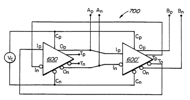
Modified differential amplifiers 600, 600' can be
connected as shown in Figure 7 to construct a resonant
circuit in the form of a modified resonator 700. In
particular, the input terminals Ip, In of the first
amplifier 600 are cross-coupled to the tap output terminals
Tn~ Tp of the second amplifier 600~, and the input terminals
Ip, In of the second amplifier 600~ are coupled to the
output terminals Op, O~ of the first amplifier 600.
Terminals Ap, An are connected to the input terminals Ip, In
of the second amplifier 600~ and terminals Bp, Bn are
connected to the output terminals Op, n Of the second
amplifier 600' as in the differential two port
bidirectional resonator 300.
The loop gain of the modified resonator 700 is the
20 product of the gain of the first amplifier 600 between its
input terminals Ip, In and its output terminals Op, n and
the somewhat lower gain of the second amplifier 600~
between its input terminals Ip, In and its tap output
terminals Tp, Tn. By suitable location of the tap output
25 terminals Tp, Tn~ the gain of the second amplifier 600'
between its input terminals Ip, In and its tap output
terminals Tp, Tn can be made less than unity to set the loop
gain very close to unity, thereby maximizing the ~uality
factor (Q) of the resonator 700.
The gain from terminals Ap, An to terminals Bp, sn
of the resonator 700 is the full gain of the amplifiers
600, 600~, whereas the gain from terminals Bp, Bn to
terminals Ap, ~ is the iower gain provided at the tap
WO93/19517 PCT/CA92/00534
13 21 321 07
output terminals Tp, T~ of the amplifiers 600, 600'.
Consequently the resonator 700 is a two port bidirectional
resonator having unequal gains in opposite directions.
Output signals taken from the tap output terminals
Tp, T~ are in phase with output signals taken from the
output terminals Op, n~ The modified resonator 700
resonates at the frequency for which there is a 90 degree
phase shift across each of the amplifiers 600, 600'.
Signals at the ports Ap, A.~ and Bp, Bn have a quadrature
phase relationship at resonance.
When the resonators 300 of the multiple resonator
VCO 500 of Figure 5 are replaced by modified resonators 700
as described above, the loop gain of each resonator 700 is
lower, but the ring gain of the multiple resonator circuit
is substantially unchanged. Consequently, the ring gain of
the multiple resonator circuit now exceeds the combined
loop gain of the resonators 700 and much higher quality
20 ~actors ~Q) closer to the theoretical values can be
obtained.
As noted above, the quality factor (Q) can be
maximized ky setting the combined loop gain of the
amplifiers 600, 600~ near unity by connecting to the tap
outputs Tn~ Tp of the second amplifier 600~ in each
resonator 700. In most conventional ring oscillator
designs, setting the loop gains near unity jeopardizes
reliable oscillation since greater than unity gain is
required for oscillator start up. However, because the
ring gain can be maintained significantly higher than unity
while setting the loop gains of each resonator 700 near
unity in this design, high quality factors (Q) can be
obtained without jeopardizing reliable oscillation.
~5
WO93/19517 PCT/CA92/00534
~ ~ 3 ~
14
The amplifier gains can arift due ~o temperature
variations, and this can jeopardize quality factor (Q)
enhancement. To compensate for such effects, the multiple
resonator VCO 500 using modified resonators 700 may further
5 comprise a current source controller in the form of a
circuit 800 as shown in Figure 8 for controlling the bias
current provided by each current source 50 of each
differential amplifier 600. The current source control
circuit 800 comprises two bipolar transistors 81, 82 and a
0 load resistor 83 which are coupled to the current sources
50 (implemented here as further bipolar transistors) in a
standard current mirror configuration so that the current
supplied by each current source 50 matches the collector
current of transistor 81. The current source control
circuit 800 further comprises a third bipolar transistor 85
which is connected to an input network comprising
resistors 86, 87 and a coupling capacitor 88, and an output
network comprising a decoupling capacitor 89. One of the
resistors 86 is larger than the other resistor 87 so that
DC base voltage of the third transistor 85 is less than
half the base voltage of the second transistor 82, and the
third transistor 85 is therefore DC-biased in its off-
state.
An amplified output of the multiple resonator VCO
500 is coupled to the base of the third transistor 85 via
the coupling capacitor 88. If the VCO output is
sufficiently large, the third transistor 85 begins to turn
on, stealing base current from the first and second
transistors 81, 82 and consequently reducing the current
supplied by each of current sources 50 to reduce the loop
gain of each resonator 700 of the multiple resonator VCO
500. The ratio of the resistances 86, 87 is selected so
that the third transistor 85 turns on when the VCO output
corresponds to a loop gain greater than unity in each
resonator 700. Consequently, the current source controller
circuit 800 sets the loop gain o. each resonator 700 near
WO93/19517 PCT/CA92/00534
21 321 07
unity for optimum quality factor enhancement. This
automatic gain control also stabilizes the output amplitude
of the multiple resonator VCO 500 at an amplitude defined
by the ratio of resistance 86 to resistance 87. A
decoupling capacitor 89 is connected across the third
transistor 85 to ensure that it responds to long term drift
of the VCO output amplitude and not to short term noise in
the control circuit 800. Because the temperature
coefficient at the collector of the third transistor 85 is
lo matched to the temperature coefficient at the base of the
second transistor 82, the temperatur~ coefficient of the
VCO output peak detection is very low, typically 0.2% per
degree Celsius.
The embodiments as described above may be modified
without departing from the inventive concept. For example,
the third transistor 85 together with its input and output
networks can be replicated for each quadrature output of
the multiresonator VCO 500 to increase the efficiency of
the current control circuit 800.
A resonator circuit having the benefits of the
resonator circuit 700 could be constructed with one
amplifier 100 having untapped load resistors and another
amplifier 600' having tapped load resistors. The amplifier
600 may be replaced with the amplifier 100 because the tap
outputs Tp, Tn of the amplifier 600 are left floating in the
resonator 700.
A resonator circuit having the benefits of the
resonator circuit 700 could also be built with two
amplifiers, each of which has only a single pair of output
terminals, provided that the two amplifiers each provide a
90 degree phase shift at substantially the same frequency
and have different gains at that frequency. For example,
the normal output terminals Op, O~ of the second amplifier
WO93/19517 PCT/CA92/00~3~
16 2~32107
600' in the resonator 700 could be eliminated, and the
second port Bp, sn could be connected to the tap output
terminals Tp, Tn of the second amplifier instead of the
normal output terminals Op, O~.
In the multiple resonator circuits 400, 500,
different numbers of resonators 300, 700 may be pro~ided to
provide different filter or vco characteristics. It can be
shown that the effective quality factor (Qn) of a multiple
resonator oscillator circuit 500 made up of n resonators
700 can be between n~ and nS/2 times the quality factor (Q)
of each resonator 700 so long as the tap ratio is suitably
selected and n is less than about Q/2. If the tap ratio is
made too large, the individual resonators 700 depart from
the ideal quadrature phase shift due to the unbalanced
bidirectional gains between the two ports. The ring
resonance then departs from the resonance of the individual
resonators 700, and the filtering effect of the resonators
700 is reduced at the ring oscillation frequency. In fact,
for n greater than 4, if the ring gain is large enough it
is possible for the ring to oscillate at a frequency
satisfying only the requirement that the total phase shift
around the ring is 360 degrees. In a practical 16
resonator ring VCO where each resonator 700 had a tap ratio
of 0.25, it was necessary to short circuit four adjacent
resonators to create a ring of four resonators 700 within a
ring o~ 16 resonators in order to make the ring oscillate
at the resonant frequency of the resonators 700. The ring
of four resonators provided additional filtering which
discriminated against lower, unwanted frequencies. Other
multiple ring arrangements are also possible.
For oscillation of multiple resonator circuits
comprising resonators connected in one or more rings, each
3s ring should comprise an integer multiple of four
resonators. Alternatively, each ring may comprise an odd
WO93/19517 PCT/CA92/00534
17 21 321 07
integer multiple of two resonators provided that one of the
resonators is cross-coupled to an adjacent resonator to
provide an additional 180 degree phase shift as required to
meet the phase shift requirements for oscillation.
5
These and other modifications are within the scope
of the invention as defined by the following claims.