Note: Descriptions are shown in the official language in which they were submitted.
2 ~ 3~4~ i
Instantaneous Phase Detecting Circuit and
Clock Recovery Signal Generating Circuit
Incorporated in Differential Demodulator
TECHNICAL FIELD
This invention relates to an instantaneous phase
detecting circuit and a clock recovery signal generating
circuit which are incorporated in a differential demodulator
for ~/4-shift QPSK signals.
BACKGROUND OF THE INVENTION
As means of digital modulation for the digital
mobile communication, the ~/4-shift QPSK method which carries
out the modulation while shifting the phase axis by ~/4 at a
time for each symbol period (two bits, for example) which
forms one data unit has been adopted on account of various
advantages attendant thereon, as discussed in "Proposal of
Linear Modulation Method for Digital Mobile Communication,"
No, 2348, written jointly by Yoshihiko Akaiwa and Yoshiki
Nagata and presented at the 1985 Consolidated National Meeting
of Electronic Communication Society (Literature 1). The
differential demodulator of the ~/4-shift QPSK method which
realizes miniaturization of the structure of modulation and
economization of the power consumption has been also proposed
in "Proposal of Linear Modulation Method for Digital Mobile
Communication~ No. 2348, written jointly by Yoshihiko Akaiwa
and Yoshiki Nagata and presented at the 1985 Consolidated
National Meeting of Electronic Communication Society "A/4-
Shift QPSK Differential Demodulator for Digital Cordless
Telephone," No. B-344, written jointly by Hiroshi Shida,
-- 1 --
27598-91
A~
2 ~1 3~442 ~1
Tsutomu Suda, and Kenzo Urabe and presented at the 1992 Spring
General Meeting of Electronic Data Communication Society
(Literature 2).
Fig. 16 represents a block diagram of the convention
differential demodulator which is disclosed in literature 2.
Now, the differential demodulator for the modulation
of a ~/4-shift QPSK signal will be described below with
reference to Fig. 16.
The differential demodulator comprises an input
terminal 1, an oscillator 2, an instantaneous phase detecting
circuit 3, a phase difference computing circuit 5, a clock
recovery circuit 7, a data regenerating circuit 8, a clock
recovery signal output terminal 9, and a regenerating data
output terminal 10.
The input terminal 1 admits a modulation wave
(carrier wave) signal (10 or 7 MHz, for example) which has
been modulated by the ~/4-shift QPSK method.
The oscillator 2 generates an electric oscillation
which is asynchronous with and substantially equal in
frequency to the modulated signal introduced to the input
terminal 1.
Fig. 17 represents a block diagram of the
conventional instantaneous phase detecting circuit 3. The
instantaneous phase detecting circuit 3 is composed of an
exclusive OR (hereinafter "EX-OR") circuit 171, a D type flip-
flop (hereinafter "DFF") circuit 172, an analog low-pass
filter (hereinafter "LPF") 173, an analog/digital converter
(hereinafter "A/D converter") 174, and a polarity switching
-- 2
27598-91
2 ~ 3 ~
circuit 175.
Now the operation of the instantaneous phase
detecting circuit 3 will be described below with reference to
Fig. 18.
Fig. 18a represents phase detection characteristics
which have been processed by the EX-OR circuit 171 and the LPF
173. In the diagram, the periods of 0 - ~, 2~ - 3~, and 4~ -
5~ have an upwardly slanting phase detection characteristic
and the periods of ~ - 2~, 3~ - 4~ and 5~ - 6~ have a
downwardly slanting phase detection characteristic
respectively to the right. Fig. 18b represents the phase
detection characteristics of the DFF circuit 172. In the
diagram, the period of 0 - ~, 2~ - 3~, and 4~ - 5~ have a
phase detection characteristic of 1 and the periods of ~ - 2~,
3~ - 4~ and 5~ - 6~ have a phase detection characteristic of
0.
The output of Fig. 18a is emitted as it is when the
output from the DFF circuit 172 is 1. The output shown in
Fig. 18a is emitted with the sign thereof inverted when the
output from the DFF circuit 172 is 0. As a result, a linear
phase detection is effected over the periods of from ~ to 3
and 3~ to 5~ as shown in Fig. 18c.
The clock recovery circuit 7 is composed of a clock
recovery signal generating circuit 71 and a digital phase
locked loop (hereinafter "DPLL") 72 as shown in Fig. 19. The
clock recovery signal generating circuit 71 is composed of
magnitude comparator 711 and a level setting circuit 712.
27598-91
A
3 ~
Fig. 20a represents the relation between the
conventional clock recovery signal and the eye pattern. The
term "eye pattern" refers to a figure derived from the loci of
a phase difference signal 6 which are described by all the
patterns possibly assumed by the phase difference signal 6.
The expression "the eye pattern is opened" as used herein
refers to the state in which figures enclosed with one phase
difference signal 6 and another phase difference signal 6
assume the shape of a human eye. The expression "the eye
pattern is closed" refers to the state in which figures
enclosed with such phase difference signals 6 assume a
decreased area.
The conventional instantaneous phase detecting
circuit 3, however, relies for phase discrimination on the DFF
circuit 172. The phase discrimination by the DFF circuit 172
lasts only during the instant of initiation of the signal
admitted into the clock terminal. When the input modulation
wave has a low frequency, namely when the frequency of the
oscillator 2 is low (as, for example, when a frequency of 1.2
MHz is used), therefore, the intervals of polarity
discrimination are too wide to coincide with the phase
discrimination of Fig. 18a. The phase discrimination in this
case, therefore, is at a disadvantage in breaking the
continuity of the phase detection in the neighbourhood of ~,
2~, ...,n~ (n for an integer).
27598-91
Further, the conventional clock recovery signal
generating circuit 71 entails jitters +~ as shown in Fig. 20b.
It has the problem of developing a deadlock and consequently
failing to effect recovery satisfactorily, when the recovered
clock signal by the DPLL 72 has a difference of 180~ from the
phase of the phase difference signal 6. The term "jitters" as
used herein refers to fluctuations of the phase difference
signal 6 relative to the clock signal.
With reference to the diagram of Fig. 20a, the
jitters are substantially effaced by the setting detection
level during the period of preamble at level 2 (phase
difference of ~/4) and returning the detection level to level
1 (phase difference of 0) after termination of the period of
preamble. This method, however, entails the necessity of
discerning whether the data currently received are those of
preamble, those of UW, or those of data proper. The
discrimination of sorts of data proves appreciably difficult
and requires use of such an external circuit as a
microprocessor and can never be realized by a simple circuit
configuration. The external microprocessor is so busy in
realizing other functions of processing that it cannot be
easily utilized for discriminating between sorts of data. As
a result, it is difficult to adopt the method which resorts to
switching the set levels depending on the sorts of data
mentioned above.
A' 27598-gl
It is an object of this invention to provide an
instantaneous phase detecting circuit which precludes
discontinuation of phase and gives rise to no inconvenience in
response to a decrease in the frequency of the input
modulation wave. It is another object of this invention to
provide an instantaneous phase detecting circuit which is
composed of invariably digital circuits and has no use for the
analog LPF 173 and the A/D converter 174 which have been
heretofore found as indispensable components.
It is a further object of this invention to provide
a clock recovery signal generating circuit which generates
such a clock recovery signal as is capable of ideally
effecting recovery at the time that the DPLL leads in a clock
signal or even after it has led in the clock signal.
SUMM~RY OF THE INVENTION
First, the instantaneous phase detecting circuit of
this invention is characterized by comprising a first logic
arithmetic circuit for admitting a modulation wave signal and
a carrier, performing a logical operation using the two input
signals, and emitting a first result of arithmetic operation,
a second logic arithmetic circuit for admitting the modulation
wave signal and a signal having the phase of the carrier
delayed by a fixed period, performing a logical operation
using the two input signals, and emitting a second result of
the arithmetic operation, a first phase detecting circuit for
admitting the first result of the arithmetic operation and the
carrier, detecting the phase of the first result of the
arithmetic operation, and emitting a first result of
-- 6
27598-91
A
detection, a second phase detecting circuit for admitting the
second result of the arithmetic operation and the carrier,
detecting the phase of the second result of the arithmetic
operation, and emitting a second result of detection, and a
third logic arithmetic circuit for admitting the first and the
second result of detection and comparing the two input signals
by the use of the deviation of period between the two input
signals thereby detecting the phase of the modulation wave
signal.
The clock recovery signal generating circuit of this
invention for the generation of a clock recovery signal is
characterized by comprising a plurality of detection axis
cross detecting means having detection axes varied in
magnitude and severally serving to admit a phase difference
signal and detect the time at which the phase difference
signal crosses the detection axis of a prescribed magnitude,
locus sorting means for discriminating and sorting the locus
of a change in the phase difference signal based on the data
of timing obtained by the detection axis cross detecting means
and emitting a timing adjusting signal in conformity with the
result of the sortation, and timing control means for
generating a clock regenerating signal by correcting the
detection timing obtained by one of the plurality of detection
axis cross detecting means designated by the timing adjusting
signal with the time designated by the timing adjusting
signal.
The clock recovery signal generating circuits
according to the present invention are constructed as follows.
-- 7
_ 27598-91
~ 3 ~
Specifically, they each comprise a plurality of
detection axis cross detecting means having detection axes
varied in magnitude and serving to detect the time at which
the phase difference signal crosses the detection axis of a
prescribed magnitude, a locus sorting means for discriminating
and sorting the locus of a change in the phase difference
signal based on the data on detection timing obtained by the
detection axis cross detecting means and emitting a timing
adjusting signal in conformity with the result of the sorting
operation, and a timing control means for correcting the
detection timing obtained by one of the plurality of detection
axis cross detecting means designated by the timing adjusting
signal with the time designated by the timing adjusting signal
and using the result of the correction as a phase signal for
clock recovery.
It is desirable that the construction described
above is further provided with phase difference discriminating
means capable of detecting the fact that the difference
between the phase of the recovered clock signal and the phase
of the clock recovery phase signal has fallen below a
prescribed magnitude and, at the same time, the locus sorting
means is so adapted as to effect the relevant processing
exclusively by the use of the detection timing obtained by one
of the plurality of detection axis cross detecting means when
the phase discriminating means has performed an action of
detection.
27598-91
A
In the clock recovery signal generating circuit of
this invention, the plurality of detection axis cross
detecting means severally detect the times at which the phase
difference signal admitted in the circuit crosses the
detection axes of magnitudes prescribed severally therefor and
inform the locus sorting means of the detected times. The
locus sorting means discriminates and sorts the locus of a
change in the phase difference signal based on the times
detected by the detection axis cross detecting means and
issues a timing adjusting signal in conformity with the result
of the sorting operation to the timing control means. The
timing control means corrects the detection timing obtained by
one of the detection axis cross detecting means designated by
the timing adjusting signal with the time designated by the
timing adjusting signal and delivers the result of the
correction as a phase signal for clock regeneration to the
DPPL.
In such a communication system as is adapted to
operate by the transmission of a fixed pattern for clock
recovery, for example, the timing control circuit is enabled
by the adjustment with the timing adjusting signal to emit a
phase signal for clock recovery during the period of the fixed
pattern when the locus sorting means is caused in advance to
learn how to discriminate the period of this fixed pattern
from any other period. Even during any other period than the
period of the fixed pattern, the phase signal for clock
recovery free from the jitter can be emitted with high
probability, depending on the setting of the locus sorting.
g
27598-91
A
2 ~
As a result, the phase of the clock signal to be emitted from
the DPLL gains in desirability and stability.
Here, phase difference discriminating means capable
of detecting the fact that the difference between the phase of
the recovered clock signal and the phase of the clock recovery
phase signal has fallen below a prescribed magnitude is
provided additionally and the locus sorting means is so
adapted as to effect the relevant processing by exclusively
using the detection timing obtained by one of the plurality of
detection axis cross detecting means when the phase difference
discriminating means has performed an action of detection. As
a result, the phase of the clock signal can be quickly
incorporated into the phase of the phase difference signal
and, at the same time, the stabilization of the clock signal
thus incorporated is realized with exalted infallibility.
BRIEF DESCRIPTION OF THE DRAWINGS
Fig. 1 is a block diagram illustrating an example of
the instantaneous phase detecting circuit of the present
lnvent lon .
Fig. 2 is a table showing an arithmetic operation
pattern of a comparison circuit of the present invention.
Figs. 3a, 3b and 3c are graphs showing a first and a
second phase detection characteristic obtained by a motion
averaging filter circuit and the result of a processing with
the instantaneous phase detecting circuit of the present
invention.
Fig. 4 is a block diagram illustrating a first
example of the clock recovery signal generating circuit of the
-- 10 --
27598-91
A
present invention.
Fig. 5 is a diagram showing the data to be used in
the present invention.
Fig. 6 is a diagram showing the conditions of
detection and the timing adjusting outputs.
Figs. 7a, 7b and 7c are diagrams showing the locus
pattern of a phase difference signal, the output timing
adjustment of a clock recovery pulse and the output timing
respectively.
Fig. 8a is a diagram showing the locus pattern of a
phase difference signal.
Fig. 8b is a diagram showing the locus pattern of a
phase difference signal.
Fig. 8c is a diagram showing the locus pattern of a
phase difference signal.
Fig. 8d is a diagram showing the locus pattern of a
phase difference signal.
Fig. 8e is a diagram showing the locus pattern of a
phase difference signal.
Fig. 9 is a block diagram illustrating a second
example of the clock recovery signal generating circuit of the
present invention.
Fig. 10 is a diagram showing the conditions of
detection and the timing adjusting output.
Fig. 11 is a block diagram illustrating a third
example of the clock recovery signal generating circuit of the
present invention.
27598-91
A
Fig. 12 is a block diagram illustrating a fourth
example of the clock recovery signal generating circuit of the
present invention.
Figs. 13a-13g are diagrams showing the locus pattern
of a phase difference signal and the timing of generation of a
pulse.
Figs. 14a-14m are diagrams showing the locus pattern
of a phase difference signal and the timing of generation of a
pulse.
Figs. 15a, 15b, 15c, and 15d are diagrams showing
the present clock signal and the clock signals delayed by ~/4
and advanced by ~/4 respectively from the present clock
signal.
Fig. 16 is a block diagram illustrating a
conventional differential demodulator.
Fig. 17 is a block diagram illustrating a
conventional instantaneous phase detecting circuit.
Figs. 18a, 18b and 18c are diagrams showing the
phase detection characteristic resulting from the processing
by an EX-OR circuit and an LPF, the phase detection
characteristic of a DFF circuit, and a linear phase detection
characteristic respectively.
Fig. 19 is a diagram showing a conventional clock
recovery circuit.
Figs. 2Oa and 2Ob are diagrams showing the locus
pattern of a phase difference signal and the output timing of
a conventional clock recovery signal respectively.
27598-91
BEST MODE OF EMBODYING THE INVENTION
First, an example of the instantaneous phase
detecting circuit of the present invention will be explained
in detail below with reference to the accompanying drawings.
Fig. 1 is a block diagram illustrating in detail the
construction of an instantaneous phase detecting
27598-91
2132442
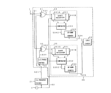
circuit 3A of the present invention. The instantaneous
phase detecting circuit 3A is composed of a 1/n
frequency divider 21, EX-OR circuits 31 and 32, a ~/2
phase-shifter 33, motion averaging filters 34 and 35,
and a logic circuit 36.
The motion averaging filter 34 is composed of an N-
stage shift register 341, a comparator 342, and an up-
down counter 343.
Similarly, the motion averaging filter 35 is
composed of an N-stage shift register 351, a comparator
352, and an up-down counter 353.
To the 1/n frequency divider 21 is applied a
carrier S2 generated from an oscillator 2. The l/n
frequency divider 21 serves to divide the carrier S2
into 1/n frequency. Here, the l/n frequency is
substantially equal to the frequency of a modulation
wave signal Sl applied through an input terminal 1.
Then, the 1/n frequency divider 21 issues a signal S21
divided into the 1/n frequency to the EX-OR circuit 31
and the ~/2 phase-shifter 33.
To the ~/2 phase-shifter 33 is applied the signal
S21 divided into the 1/n frequency. The ~/2 phase-
shifter 33 shifts the phase of the received signal S21
with a delay of ~/2. Then, the ~/2 phase-shifter 33
generates a signal S33 having a phase delayed by ~/2 to
the EX-OR circuit 32.
The EX-OR circuits 31 and 32 are severally composed
- 14 -
21324~2
of electric circuits, semiconductor elements, etc.
To the EX-OR circuit 31 are applied a modulation
wave signal Sl and the signal S21 divided into the l/n
frequency. Then, the EX-OR circuit 31 carries out an
exclusive logical sum operation on the input modulation
wave signal Sl and the signal S21 divided into the l/n
frequency. The EX-OR circuit 31 subsequently issues the
result of the exclusive logical sum operation as a
signal S31 to the motion averaging filter 34.
To the EX-OR circuit 32 are inJected the modulation
wave signal Sl and the signal S33 having a phase delayed
by ~/2. Then, the EX-OR circuit 32 carries out an
exclusive logical sum operation on the input modulation
wave signal Sl and the signal S33 having a phase delayed
by ~/2. The EX-OR circuit 32 subsequently issues the
result of the exclusive logical sum operation as a
signal S32 to the motion averaging filter 35.
The motion averaging filter 34 is composed of the
N-stage shift register 341, the comparator 342, and the
up-down counter 343. Here, N stands for a natural
number.
To the N-stage shift register 341 are applied the
result of arithmetic operation S31 and the carrier S2.
Here, the carrier S2 is used as a master clock for
driving the motion averaging filter 34. Then, the N-
stage shift register 341 issues the contents of a first
stage 341A and those of an N'th stage 341B to the
- 15 -
comparator 342. This issuance of the contents to the
comparator 342 is carried out in accordance with the
timing of the carrier S2 as the master clock.
To the comparator 342 are applied the carrier S2
and the contents of the first stage 341A of the N-stage
shift register 341 and those of the N'th stage 341B.
Here again, the carrier S2 is utilized as a master
clock. After the arithmetic operations mentioned above
have been completed, the comparator 342 issues the
result of the arithmetic operations as a signal S342 to
the up-down counter 343.
The arithmetical operation which is performed by
the comparator 342 will be explained below. The
arithmetical processing so fulfilled by the comparator
342 is broadly divided into the following three types.
(1) The comparator 342 causes a +1 up count in the
up-down counter 343 when the first stage 341A of the N-
stage shift register 341 has an input of 1 and the N'th
stage 341B thereof has a content of 0.
(2) The comparator 342 causes a -1 down count in
the up-down counter 343 when the first stage 341A of the
N-stage shift register 341 has an input of 0 and the
N'th stage 341B thereof has a content of 1.
(3) The comparator 342 causes no change in the up-
down counter 343 when the content of the first stage
341A of the N-stage shift register 341 and that of the
- 16 -
27598-91
,j, /
2132~42
N'th stage 341B thereof are equal (namely when the first
stage 341A has a content of 0 and the N'th stage 3418
has a content of 0 or when the first stage 341A has a
content of 1 and the N'th stage 341B has a content of
1).
When the comparator 342 has performed the
arithmetical processing described above for one timing
of the master clock, the number of "l's" existing in the
second through N'th stages of the N-stage shift register
341 is displayed in the up-down counter 343. The
content of the up-down counter 343, therefore, indicates
the outcome of the processing performed on the output
from the EX-OR circuit 31 by the motion averaging filter
which functions to average the time constant, T = (N -
1)/fc. In the formula, N stands for the number of
stages in the shift register 341 and fc for the
frequency of the oscillator 2.
The up-down counter 343 generates a phase detection
characteristic (numerical value counted as instructed by
the comparator 342) S34 as an output to the logic
circuit 36.
Incidentally, one example of the motion averaging
filter circuit 34 is disclosed in JP-B-01-38,244.
To the N-stage shift register 351 are applied the
result of arithmetic operation S32 and the carrier S2.
In this case, the carrier S2 is utilized as a master
lock for driving the motion averaging filter circuit 35.
2132442
Then, the N-stage shift register 351 issues the content
of the first stage 351A and the content of the N'th
stage 351B as outputs to the comparator 352. This
issuance of the outputs to the comparator 352 is carried
out in accordance with the timing of the carrier S2 as a
master clock.
To the comparator 352 are applied the carrier S2
and the content of the first stage 351A and that of the
N'th stage 351B of the N-stage shift register 351.
Again in this case, the carrier S2 is utilized as a
master clock. The comparator 352 issues the result of
arithmetic operation S352 as an output to the up-down
counter 353.
The operation of the comparator 352 is identical
with that of the comparator 342.
The up-down counter 353 issues a phase detection
characteristic (numerical value counted as instructed by
the comparator 352) S35 as an output to the logic
circuit 36.
To the logic circuit 36 are applied the phase
detection characteristic S34 and the phase detection
characteristic S35. In the logic circuit 36, the sign
of the input phase detection characteristic S34 is
reversed on the basis of the input phase detection
characteristic S35. When the input phase detection
characteristic S35 has a minus sign, for example, the
logic circuit 36 reverses the sign of the input phase
- 18 -
detection characteristic to minus and emits the outcome
of the sign reversion as an output. When the input
phase detection characteristic S35 has a plus sign, the
logic circuit 36 generates the input phase detection
characteristic S34 in its unaltered form as an output.
Now, the operation of the instantaneous phase
detecting circuit of the present invention will be
described below with reference to Figs. 3a - 3c.
Fig. 3a is a graph showing the phase detection
characteristic S34 which is obtained by the motion
averaging filter 34. In Fig. 3a, the periods of 0 - ~,
2~ - 3~, and 4~ - 5~ describe straight lines inclined
upward to the right and indicating an increase of the
content of the up-down counter 343 from 0 to N - 1. The
periods of ~ - 2~, 3~ - 4~, and 5~ - 6~ describe
straight lines inclined downward to the right and
indicating a decrease of the content of the up-down
counter 343 from N - 1 to 0. In the graph, the
horizontal axis is the scale of the phase difference
between the signal S21 divided into the 1/n frequency
and the modulation wave signal S1 and the vertical axis
is the scale of the content of the up-down counter 343.
Fig. 3b is a graph showing the phase detection
characteristic S35 which is obtained by the motion
averaging filter 35. The phase detection characteristic
S35 shown in Fig. 3b is delayed by a phase of ~/2 from
the phase detection characteristic S34 shown in Fig. 3a.
-- 19 --
27598-91
A
2132~42
This delay of phase is due to the ~/2 phase-shifter 33.
In Fig. 3b, the period of 0 - ~/2 describes a
straight line inclined upward to the right and
indicating an increase of the content of the up-down
counter 353 from N/2 to N - 1. The periods of (3~/2) -
(5n/2) and (7~/2) - (9~/2) describe straight lines
inclined upward to the right and indicating an increase
of the content of the up-down counter 353 from 0 to N -
1. The period of (11~/2) - 6~ describes a straight line
inclined upward to the right and indicating an increase
of the content of the up-down counter 353 from 0 to N/2.
Then, the periods of ~/2 - (3~/2), (5~/2) - (7~/2), and
(9~/2) - (11~/2) describe straight lines inclined
downward to the right and indicating a decrease of the
content of the up-down counter 353 from N - 1 to 0. In
the graph, the horizontal axis is the scale of the phase
difference between the signal S21 divided into the 1/n
frequency and the modulation wave signal S1 and the
vertical axis is the scale of the content of the up-down
counter 353.
The logic circuit 36 treats the periods of 0 - ~,
2n - 3~, and 4~ - 5~ as positive periods and the periods
of ~ - 2~, 3~ - 4~, and 5~ - 6~ as negative periods on
the basis of N/2 in the content of the up-down counter
353.
In the periods discriminated as positive periods in
Fig. 3b, the logic circuit 36 generates the phase
- 20 -
detection characteristic S34 shown in Fig. 3a in its
unaltered form as an output. Then, in the periods
discriminated as negative periods in Fig. 3b, the logic
circuit 36 emits the phase detection characteristic S34
shown in Fig. 3a with an inverted sign as an output.
The graph shown in Fig. 3c is consequently
obtained. In Fig. 3c, the period of O - ~ describes a
straight line inclined upward to the right and
indicating an increase of the phase from O to ~. The
periods of ~ - 3n and 3~ - 5~ describe straight lines
inclined upward to the right and indicating an increase
of the phase from -~ to n. Then, the period of 5~ - 6
describes a straight line inclined upward to the right
and indicating an increase of the phase from -~ to 0.
In consequence of the operation described above,
the instantaneous phase detecting circuit of the present
invention processes the digital phase modulation wave by
the use of the two EX-OR circuits, the motion averaging
filter circuit, and the logic circuit so as to have one
phase delayed by ~/2 from the other phase. Owing to
this processing, the instantaneous phase detecting
circuit of this invention does not easily encounter
discontinuation of phase detection even when the
modulation wave to be received as an input has such a
low frequency as 1 or 2 MHz. The in~tantaneous phase
detecting circuit of this invention, therefore, is
capable of effecting phase detection with accuracy.
27598-91
~'
This invention does not limit the delay of phase to
~/2. It can be likewise embodied even when the delay is 0,
~/4 etc., for example. When the delay is so changed, the
construction of the logic circuit 36 may be suitably altered
in conformity with the particular phase delay.
Since the instantaneous phase detecting circuit of
this invention uses a motion averaging filter for its
configuration as described above, it can be digitized, adapted
for integration of the circuit, and allowed to enjoy a cut in
cost. The devices which use the instantaneous phase detecting
circuit of this invention, therefore, are at an advantage in
attaining reduction in size and weight.
Now, the first example of the clock recovery signal
generating circuit of the present invention will be described
below with reference to the annexed drawings. Fig. 4 is a
block diagram illustrating in detail the construction of the
first example.
A clock recovery circuit 7A iS composed of a clock
recovery signal generating circuit 71A and the DPLL (digital
20 phase locked loop) circuit 72.
The clock recovery signal generating circuit 71A is
composed of magnitude comparators 701 and 703, level setting
circuits 702 and 704, a locus sorting circuit 710, and a
timing control circuit 707. The locus sorting circuit 710 is
composed of a timer circuit 705
- 22 -
27598 - 91
2132~42
and a discriminating circuit 706. Here, the magnitude
comparator 701 and the level setting circuit 702 are
disposed correspondingly. The magnitude comparator 703
and the level setting circuit 704 are also disposed
correspondingly.
Now, the construction of the clock recovery signal
generating circuit 71A will be described below.
The magnitude comparators 701 and 703 are
comparators of a sort for use with digital circuits.
The magnitude comparators 701 and 703 are circuits for
generating an instantaneous pulse when the phase
difference signal 6 received as an input equals the
magnitude of detection level (detection axis) set in
advance by the corresponding level setting circuits 702
and 704.
The level setting circuit 702 and 704 set the
magnitude of detection level (detection axis) and
generate the magnitude of detection level as an output
to the magnitude comparators 701 and 703.
To the magnitude comparator 701 are injected the
phase difference signal 6 and a magnitude of detection
level S702 issued from the level setting circuit 702.
The magnitude comparator 701 compares the input phase
difference signal 6 with an input magnitude of detection
level S701 and determines whether or not they are equal.
The magnitude comparator 701 generates the pulse S701
(hereinafter the pulse S701 issued from the magnitude
comparator 701 will be referred to briefly as "level 1
cross pulse S701") only when it has discriminated the
equality between the input phase difference signal 6 and
the input magnitude of detection level S702. When the
magnitude comparator 701 has issued the level 1 cross
pulse S701, the magnitude comparator 701 generates the
level 1 cross pulse S701 as an output to the timing
control circuit 707 and the locus sorting circuit 710.
. Here, the level setting circuit 702 has level 1
corresponding to a phase difference of 0 set as the
magnitude of detection level S702 trefer to Fig. 6a and
Fig~- 7a, 7b, and 7c which will be specifically described
hereinafter).
Similarly to the magnitude comparator 703 are
applied the phase difference signal 6 and a magnitude of
detection level S704 to be issued from the level setting
circuit 704. The magnitude comparator 703 determines
whether or not the input phase difference signal 6 and
the input magnitude of detection level S704 are equal.
The magnitude comparator 703 issues a pulse S703
(hereinafter the pulse S703 issued by the magnitude
comparator 703 will be referred to briefly as "level 0
cross pulse S703") only when it has discriminated the
equality between the input phase difference signal 6 and
the input magnitude of detection level S704. When the
magnitude comparator 703 has issued the level 0 cross
pulse S703, the magnitude comparator 703 issues the
- 24 -
27598-91
4 ~
level 0 cross pulse S703 as an output to the timing
control circuit 707 and the locus sorting circuit 710.
Here, the level setting circuit 704 has a level 0
corresponding to the phase difference of ~/2 set as the
magnitude of detection level S704 (refer to Fig. 6a and
Figs. 7a, 7b, and 7c which will be specifically described
hereinbelow).
The locus sorting circuit 710 is composed of the
timer circuit 705 and the discriminating circuit 706.
The locus sorting circuit 710 discriminates and sorts
the locus of a change in the phase difference signal 6
on the basis of the level 1 cross pulse S701 and the
level 0 cross pulse S703. Then, the locus sorting
circuit 710 generates a timing adjusting signal S706
corresponding to the discriminated sort as an output to
the timing control circuit 707.
To the timer circuit 705 are applied the level 1
cross pulse S701 and the level 0 cross pulse S703. The
timer circuit 705 starts the timer counting when it has
received either of the level 1 cross pulse S701 and the
level 0 cross pulse S703 as an input. Then, the timer
circuit 705 causes the timer to cease the counting when
either of the leveL 1 cross pulse S701 and the level 0
cross pulse S703 is introduced as an input within a
fixed interval after the start of the timer counting.
Here, one and the same pulse may be used for starting
and terminating the timer counting. For example, the
- 25 -
27598-91
~132~2
level 0 cross pulse S703 may be applied to start the
timer counting and the level 0 cross pulse S703 may be
also applied to terminate the timer counting. There are
times when the pulse for terminating the timer counting
is not applied within the fixed interval after the pulse
for starting the timer counting has been injected. The
timer circuit 705, therefore, is so constructed that the
timer counting may be automatically terminated and reset
after the elapse of the fixed interval. Then, the timer
circuit 705 issues a count data (time counted) S705 as
an output to the discriminating circuit 706 and resets
the timer.
Here, the timer circuit 705 resets the timer with
the level 0 cross pulse S701 and starts the clocking all
over again from the beginning when the first pulse to be
applied after the application of the level 0 cross pulse
S701 happens to be the level 0 cross pulse S701.
The timer circuit 705 resets the timer with the
level 1 cross pulse S703 and starts the clocking all
over again from the beginning when the first pulse to be
applied after the application of the level 1 cross pulse
S703 happens to be the level 1 cross pulse S703.
To the discriminating circuit 706 is applied the
count data S705. The discriminating circuit 706
determines whether or not the input count data S705
satisfies any of the conditions for detection stored in
advance in the discriminating circuit 706 (refer to Fig.
6a which will be specifically described hereinbelow).
Then, the discriminating circuit 706 generates as an
output to the timing control circuit 707 the timing
adjusting signal S706 which corresponds to the
condition of detection found to be satisfied by the
input count data S705.
To the timing control circuit 707 are applied the
level 1 cross pulse S701, the level 0 cross pulse S703,
and the timing adjusting signal S706. The timing
control circuit 707 generates a clock recovery signal
S707 as an output to the DPLL circuit 72 in accordance
with the input timing adjusting signal S706 (refer to
Fig. 6a which will be described specifically
hereinbelow).
Now, the operations of the circuits within the
clock recovery signal generating circuit 71A will be
described and, through the description of these
operations, the functions of the timer circuit 705, the
discriminating circuit 706, and the timing control
circuit 707 will be delineated.
In the first example, the two detection levels of
level 0 and level 1 are set in the level setting
circuits. The magnitude comparators severally issue a
pulse at the moment that the phase difference signal 6
becomes equal to the magnitude of detection level. The
locus sorting circuit 710 estimates what sort of a locus
has been described by the phase difference signal 6 on
- 27 -
27598-91
2132~2
the basis of the state of application of the pulse. In
accordance with the estimated locus, the timing control
circuit 707 selects the time preceding the generation of
the clock recovery signal S707. The timing control
circuit 707 effects the generation of the clock recovery
signal S707 in accordance with the result of the
selection. The first example operates by this method.
Here, the two magnitudes of detection level are the
level 1 detection level S702 corresponding to the phase
difference of 0 and the level 0 detection level S704
corresponding to the phase difference of ~/2. The
magnitude of detection level S702 is set in the level
setting circuit 702 and the magnitude of detection level
S704 in the level setting circuit 704.
To the magnitude comparator 701 are applied the
phase difference signal 6 and the magnitude of detection
level S702. The magnitude comparator 701 determines
whether or not the phase difference signal 6 equals the
detection level S702. When it has determined that the
phase difference signal 6 and the magnitude of detection
level S702 are equal, the magnitude comparator 701
generates the level 1 cross pulse S701. Then, the
magnitude comparator 701 emits the level 1 cross pulse
S701 so generated as an output to the timing control
circuit 707 and the locus sorting circuit 710. When the
magnitude comparator 701 has deteL ;ne~ that the phase
difference signal 6 and the magnitude of detection level
- 28 -
2132~42
S702 are not equal, it does not generate the level 1
cross pulse S701.
To the magnitude comparator 703 are applied the
phase difference signal 6 and the detection level S704.
The magnitude comparator 703 determines whether or not
the phase difference signal 6 and the magnitude of
detection level S704 are equal. When the magnitude
comparator 703 has determined that the phase difference
signal 6 and the magnitude of detection level S704 are
equal, it generates the level 0 cross pulse S703.
Then, the magnitude comparator 703 emits the level 0
cross pulse S703 so generated as an output to the timing
control circuit 707 and the locus sorting circuit 710.
When the magnitude comparator 703 has determined that
the phase difference signal 6 and the magnitude of
detection level S704 are not equal, it does not generate
the level 0 cross pulse S703.
Now, the data to be used in the present invention
will be described below with reference to Fig. 5.
The data is composed of a preamble part, a UW part,
and a data proper.
The preamble part has the input of a preamble
pattern. For example, it has the input of repetitions
of "1001" in such a manner as "10011001...1001."
The UW part has the input of a sign designating the
head of a data.
The data proper has the input of a data which is
- 29 -
2132442
desired to be transmitted.
Fig. 6a and Fig. 7 are diagrams showing the
operations of the locus sorting circuit 710 and the
timing control circuit 707 in the first example.
The time T denotes the duration of an operation
equivalent to one symbol of data (time equal to 360~).
The fixed time Td denotes the duration of an
operation for determining whether or not the phase
difference signal 6 is a pulse in the period of preamble
(time equal to 150~, for example).
The time tO denotes the duration of an operation
enabling the timing control circuit 707 to adjust the
timing of emitting the clock recovery signal S707 (time
equal to 60~, for example).
Now, the method for estimating the locus of the
phase difference signal 6 will be described below with
reference to Fig. 6a. Fig. 6a is a diagram showing the
operations of the timer circuit 705 and the
discriminating circuit 706 of the locus sorting circuit
710.
Detection No. 1 is obtained only when the
conditions shown in 1 to 5 below are wholly satisfied
sequentially in the order mentioned.
1. The timer circuit 705 admits the level 0 cross
pulse S703 as an input.
2. The timer circuit 705 starts counting (clocking
time).
- 30 -
2132442
3. The timer circuit 705 admits the level 1 cross
pulse S701 as an input.
4. The timer circuit 705 terminates the counting
(clocking of time).
5. The discriminating circuit 706 compares the
count data (clock reading) S705 with the fixed time Td
set in advance and finds that the count data is shorter
than the fixed time Td.
When Detection No. 1 is obtained, the
discriminating circuit 706 generates the timing
adjusting signal S706 as an output to the timing control
circuit 707. Then, after the elapse of the time ¦tO +
T/2¦ following the time of application of the level 0
cross pulse S703 into the locus sorting circuit 710, the
timing adjusting signal S706 causes the t;~;ng control
circuit 707 to issue the clock recovery signal S707 to
the DPLL circuit 72.
Detection No. 2 is obtained only when the
conditions shown in 1 to 5 below are wholly satisfied
sequentially in the order mentioned.
1. The timer circuit 705 admits the level 1 cross
pulse S701 as an input.
2. The timer circuit 705 starts counting (clocking
time).
3. The timer circuit 705 admits the level 0 cross
pulse S703 as an input.
4. The timer circuit 705 terminates the counting
- 31 -
2132~42
(clocking of time).
5. The discriminating circuit 706 compares the
count data (clock re~ing) S705 with the fixed time Td
set in advance and finds that the count data (clock
reading) S705 is shorter than the fixed time Td.
When Detection No. 2 is obtained, the
discriminating circuit 706 emits the timing adjusting
signal S706 as an output to the ti~;ng control circuit
707. Then, after the elapse of the time ¦tO + T/2¦
following the time of injection of the level 1 cross
pulse S703 into the locus sorting circuit 710, the
timing adjusting signal S706 causes the timing control
circuit 707 to issue the clock recovery signal S707 to
the DPLL circuit 72.
Detection No. 3 is obtained only when the
conditions shown in 1 to 3 below are wholly satisfied
sequentially in the order mentioned.
1. The timer circuit 705 admits the level 1 cross
pulse S701 as an input.
2. The timer circuit 705 starts counting (clocking
time).
3. The timer circuit 705 does not admit the level
0 cross pulse S703 within the fixed time Td.
When Detection No. 3 is obtained, the
discriminating circuit 706 generates the timing
adjusting signal S706 as an output to the timing control
circuit 707. Then, after the elapse of the time ¦T/2¦
- 32 -
following the time of injection of the level 1 cross pulse
S703 into the locus sorting circuit 710, the timing adjusting
signal S706 causes the timing control circuit 707 to issue the
clock recovery signal S707 to the DPLL circuit 72.
Figs, 7a, 7b and 7c are explanatory diagrams showing
sorting of the loci of the phase difference signal (detection
of locus) and an explanatory diagram of the adjustment of the
output timing of the clock regenerating pulse shown in Fig. 5.
The bold line in Fig. 7a represents the same locus
"10011001 .... 1001" of the phase difference signal 6 during
the period of preamble as shown in Fig. 2Oa. In the case of
the ~/4-shift QPSK signal, it is not the magnitude of phase
difference itself of the phase difference signal 6 but the
locus of the phase difference signal 6 that represents data
value.
Here, ~, ~/2, ~/4, O, -~/2, and -~ in the vertical
axis of the graph denote magnitudes of phase difference. In
Fig. 7a, the times a and e represent intersections of the
phase difference signal 6 and the phase difference ~/2 during
the period of preamble. The times b and d represent
intersections of the phase difference signal 6 and the phase
difference O during the period of preamble.
First, the case in which Detection No. 1 is obtained
will be described below with reference to Fig.
27598-91
2132492
7a.
The phase difference signal 6 crosses the detection
level magnitude at the time a during the period of
preamble. Then, the timer circuit 705 of the locus
sorting circuit 710 admits the level 0 cross pulse S703
as an input from the magnitude comparator 703 and starts
counting. Then, the phase difference signal 6 during
the period of preamble crosses the detection level
magnitude at the time b. The timer circuit 705
consequently admits the level 1 cross pulse S701 as an
input from the magnitude comparator 701 within the fixed
time Td from the time point a and terminates the
counting (at the time point b). Here, the
discriminating circuit 705 determines that the count
data S705 is shorter than the fixed time Td. Detection
No. 1 is obtained in consequence of the operation
described above.
At the time c which terminates the duration of ¦tO
~ T/2¦ starting from the time a, the discriminating
circuit 706 generates as an output to the timing control
circuit 707 the timing adjusting signal S706 instructing
the clock recovery signal S707 as an output to the DPLL
circuit 72 (refer to Fig. 7b).
Then, the case in which Detection No. 2 is obtained
will be described below with reference to Fig. 7a.
The phase difference signal 6 during the period of
preamble crosses the detection level magnitude at the
- 34 -
21329 12
time d. As a result, the timer circuit 705 of the locus
sorting circuit 710 admits the level 1 cross pulse S701
as an input from the magnitude comparator 701 and starts
counting. Then, the phase difference signal 6 during
the period of preamble crosses the detection level
magnitude at the time e. As a result, the timer circuit
705 admits the level 0 cross pulse S703 as an input from
the magnitude comparator 703 within the fixed time Td
from the time d and terminates the counting (at the time
e). Here, the discriminating circuit 705 determines
that the count data S705 is shorter than the fixed time
Td. Detection No. 2 is obtained in consequence of the
operation described above.
At the time point f which terminates the duration
of ¦tO + T/2¦ starting from the time d, the
discriminating circuit 706 generates as an output to the
timing control circuit 707 the timing adjusting signal
S706 instructing the clock recovery signal S707 as an
output to the DPLL circuit 72 (refer to Fig. 7b).
Similarly thence, the phase difference signal 6
during the period of preamble adapts the locus sorting
carrier 710 for the adjustment of timing of Detection
No. 1 and Detection No. 2. Then, from the timing
control circuit 707, the clock recovery signal S707 is
emitted at such a timing that the eye pattern may be
opened to the widest extent as illustrated in Fig. 7b
(at the time points of c and f). As a result, a clock
3 ~ G ~ 2
signal of a correct phase synchronized with this pulse
is generated from the DPLL 72 as shown in Fig. 7c.
Here, the jitter ~ is set at 0 as shown in Fig.
20b. Then, the clock recovery signal of Fig. 7b is
compared with the clock recovery signal of Fig. 20b. It
is consequently found that during the period of
preamble, the phase of the clock recovery signal S707
given to the DPLL 72 is varied with an increment of T/2.
The DPLL 72, however, is capable of easily coping with
this difference by advancing the phase discrimination
within the DPLL 72 with an increment of T/2.
When the period of preamble terminates and the
period of UW or that of data proper sets in, the bit
pattern is no longer fixed. As a result, the phase
difference signal 6 assuming any of a total of 16 foci
is applied as an input to the clock recovery signal
generating circuit 71A. Detection No. 1 and Detection
No. 2 mentioned above have due respect paid to the loci
particularly during the period of preamble. Even during
the period of UW or that of data proper, the assumption
of such loci as are related to Detection No. 1 and
Detection No. 2 possibly arises. The loci related to
Detection No. 3 correspond to the period of UW and that
of data proper. The number of loci along which the
adjustment of timing is effected by Detection No. 3 is 8
as described specifically hereinafter.
Fig. 8a, Fig. 8b, Fig. 8c, Fig. 8d, and Fig. 8e aid
27598-91
2132~42
in the description of the relation of the total of 16
loci and the adjustment of output timing of the clock
recovery pulse. Now, the relation between the loci of
the phase difference signal 6 and the adjustment of
timing will be described below with reference to Fig.
8a, Fig. 8b, Fib. 8c, Fig. 8d, and Fig. 8e. For the
sake of convenience of the explanation, the total of 16
loci are depicted as divided in five diagrams.
In Fig. 8a, the two locus patterns 8a-1 and 8a-2
are indicated each with a bold line.
First, the locus pattern 8a-1 will be explained.
The timer circuit 705 of the locus sorting circuit 710
admits the level 0 cross pulse S703 as an input from the
magnitude comparator 703 and starts counting (at the
time point g). Then, within the fixed time Td from the
time point g, the timer circuit 705 admits the level 1
cross pulse S701 as an input from the magnitude
comparator 701 and terminates the counting (at the time
point h). The discriminating circuit 705 determines
that the count data S705 is shorter than the fixed time
Td. Detection No. 1 (refer to Fig. 6a) is obtained in
consequence of the operation described above.
After the elapse of the time ¦tO + T/2¦ from the
time point g, the discriminating circuit 706 emits the
timing adjusting signal S706 as an output to the timing
control circuit 707.
In the same manner as described above with respect
2132~2
to the period of preamble, the timing control circuit
707 undergoes the adjustment of timing by the locus
sorting circuit 710 and, in consequence thereof, emits
the clock recovery signal S707 at such a timing that the
eye pattern may be opened to the widest extent.
Now, the locus pattern 8a-2 will be explained
below. The timer circuit 705 of the locus sorting
circuit 710 admits the level 1 cross pulse S701 as an
input from the magnitude comparator 701 and starts
counting (at the time i). Then, within the fixed time
Td from the time i, the timer circuit 705 admits the
level 0 cross pulse S703 as an input from the magnitude
comp~rator 703 and terminates the counting (at the time
j). The discriminating circuit 705 determines that the
count data S705 is shorter than the fixed time Td.
Detection No. 2 (see Fig. 6a) is obtained in consequence
of the operation described above.
Then, after the elapse of the time ¦tO + T/2¦ from
the time i, the discriminating circuit 706 generates the
timing adjusting signal S706 as an output to the timing
control circuit 707.
In the same manner as described above with respect
to the period of preamble, the timing control circuit
707 undergoes the adjustment of timing by the locus
sorting circuit 710 and, in consequence thereof,
generates the clock recovery signal S707 at such a
timing that the eye pattern may be opened to the widest
- 38 -
2132442
extent.
In Fig. 8b, the six locus patterns 8b-1, 8b-2, 8b-
3, 8b-4, 8b-S, and 8b-6 are indicated each with a bold
line.
None of these locus patterns crosses either the 0
or the 1 detection level. In this case, none of the
conditions for detection indicated for Detection No. 1
through No. 3 in Fig. 6a is applicable. Thus, the
adjustment of timing by the locus sorting circuit 710 is
not carried out on any of these locus patterns. Then,
the timing control circuit 707 does not generate the
clock recovery signal S707.
In Fig. 8c, the two locus patterns 8c-1 and 8c-2
are indicated each with a bold line.
Now, the two locus patterns 8c-1 and 8c-2 will be
explained below. The timer circuit 705 of the locus
sorting circuit 710 admits the level 0 cross pulse S703
as an input from the magnitude comparator 703 and starts
counting (at the time point k). Within the fixed time
Td from the time point k, however, neither of these two
locus patterns 8c-1 and 8c-2 crosses either the 0 or the
1 detection level S702 or S704. Thus, none of the
conditions for detection indicated for Detection No. 1
through No. 3 in Fig. 6a is applicable. Thus, the
adjustment of timing by the locus sorting circuit 710 is
not carried out on either of these two locus patterns
8c-1 and 8c-2. Then, the timing control circuit 707
- 39 -
2132442
does not generate the clock recovery signal S707.
In Fig. 8d, the four locus patterns 8d-1, 8d-2, 8d-
3, and 8d-4 are indicated each with a bold line.
Now, the four locus patterns 8d-1, 8d-2, 8d-3, and
8d-4 will be explained below. The timer circuit 705 of
the locus sorting circuit 710 admits the level 1 cross
pulse S701 as an input from the magnitude comparator 701
and starts counting (at the time points 1, m, and n).
Within the fixed time Td from the relevant time points
(1, m, and n), however, none of the four locus patterns
8d-1, 8d-2, 8d-3, and 8d-4 crosses either of the 0 and
the 1 detection level S702 or S704.
The present case falls under the condition of
detection of Detection No. 3 of Fig. 6a. The timing
control circuit 707, therefore, undergoes the adjustment
of timing effected by the locus sorting circuit 710.
Then, the timing control circuit 707 generates the clock
recovery signal S707 after the elapse of the fixed time
T/2 from the times (1, m, and n) of crossing.
Here, the timing control circuit 707 generates the
clock recovery signal S707 with respect to the two most
gradually inclined locus patterns 8d-1 and 8d-2 in all
the four locus patterns 8d-1, 8d-2, 8d-3, and 8d-4 as
shown in Fig. 8d at such a timing that the eye pattern
may be opened to the widest extent.
Then, the timing control circuit 707 generates the clock
recovery signal S707 deviated by a fixed amount (jitter
- 40 -
2132~2
+ ~1) from the time at which the eye pattern is opened
to the widest extent with respect to the other two most
sharply inclined locus patterns 8d-3 and 8d-4.
In Fig. 8e, the two locus patterns 8e-1 and 8e-2
are indicated each with a bold line. Neither of these
locus patterns represents a signal during the period of
preamble.
First, the locus pattern 8e-1 will be explained
below. The timer circuit 705 of the locus sorting
circuit 710 admits the level 0 cross pulse S703 as an
input from the magnitude comparator 703 and starts
counting (at the time o). Then, within the fixed time
Td from the time o, the timer circuit 705 admits the
level 1 cross pulse S701 as an input from the magnitude
comparator 701 and terminates the counting (at the time
p. The discriminating circuit 705 then determines that
the count data S705 is shorter than the fixed time Td.
Detection No. 1 (refer to Fig. 6a) is obt~inP~ in
consequence of the operation described above.
Then, after the elapse of the time ¦tO + T/2¦ from
the time o, the discriminating circuit 706 generates the
timing adjusting signal S706 as an output to the timing
control circuit 707.
Now, the locus pattern 8e-2 will be explained
below. The timer circuit of the locus sorting circuit
710 admits the level 1 cross pulse S701 as an input from
the magnitude comparator 710 and starts counting (at the
- 41 -
2132442
time p). Then, within the fixed time from the time
point p, the timer circuit 705 admits the level 0 cross
pulse S703 as an input from the magnitude comparator 703
and terminates the counting (at the time q). The
discriminating circuit 705 determines that the count
data S705 is shorter than the fixed time Td. Detection
No. 2 (refer to Fig. 6a) is obtained in consequence of
the operation described above.
Then, after the elapse of the time ¦tO + T/2¦ from
the time p, the discriminating circuit 706 emits the
timing adjusting signal S706 as an output to the timing
control circuit 707.
These locus patterns, however, invariably produce a
latter cross earlier or later than the locus patterns
which mainly occur during the period of preamble shown
in Fig. 7a. Thus, the time at which the clock recovery
pulse is generated is deviated by a fixed amount (jitter
+ ~2) from the most desirable time at which the eye
pattern is opened to the widest extent.
In the clock recovery signal generating circuit 71A
of the first example, the clock recovery signal S707
having no jitter can be extracted perfectly and applied
into the DPLL 72 during the reception of the pattern of
the period of preamble as described above. Further, the
clock signal generated from the DPLL 72 can be quickly
led in at a correct phase angle and this correct phase
angle can be stably maintained.
- 42 -
2132442
Even after the pattern of the period of preamble
has ceased to exist, the clock recovery signal
generating circuit 71A of the first example can extract
the clock recovery pulse with a probability of 1/2 (8
out of 16 chances) and inject it into the DPLL 72.
Then, the clock recovery signal generating circuit 71A
can be utilized for the control of the phase of the
clock signal generated from the DPLL 72. The clock
recovery pulses which are extracted as described above
include those having jitters with a probability of 1/2
(4 out of 8 ch~nces). Even when the DPLL 72 happens to
utilize such a clock recovery pulse as entails a jitter,
this clock recovery pulse amply functions in following
the input signal because the phase error between the
regenerated clock signal and the input signal has been
fully minimized during the period of preamble.
The clock recovery signal generating circuit 7lA
described above, therefore, attains detection of the
phase of the phase difference signal 6 by utilizing the
cross phase relative to the plurality of detection
levels (detection axes). Further, the clock recovery
signal generating circuit 71A mentioned above is so
adapted as to generate clock recovery pulses having no
jitter. The clock recovery signal generating circuit
71A, therefore, is capable of quickly and correctly
synchronizing the clock signal with the phase of the
input signal during the period of preamble. Further,
- 43 -
2132~2
the clock recovery signal generating circuit 71A is
generating clock recovery signals S707 which have no
jitter. As a result, the clock recovery signal
generating circuit 71A is capable of precluding the
otherwise possible occurrence of the so-called state of
deadlock. Further, the DPLL 72 is not always required
to be provided with a device capable of precluding the
occurrence of the state of deadlock.
Besides, the clock recovery signal generating
circuit 71A mentioned above is capable of generating a
clock recovery signal S707 with a high probability even
after the period of preamble has terminated. Further,
the clock recovery signal generating circuit 71A permits
continuous follow of the clock recovery signal S707.
The clock recovery signal generating circuit 71A,
therefore, can markedly decrease the possibility of
disrupting synchronism from the conventional standard.
As a result, the DPLL 72 is enabled to generate
clock signals of ideal quality.
Further, the clock recovery signal generating
circuit 71A does not need to discriminate the origin of
the input signal to the differential demodulator between
the preamble and the UW or data proper. In addition,
the clock recovery signal generating circuit 71A can
repress the inevitable increase in the size thereof to
the smallest possible extent and, at the same time, has
no possibility of imposing any burden on an external
2132442
microprocessor.
The clock recovery signal is generated in
consequence of the operation described above.
Now, the second example of the clock recovery
signal generating circuit of this invention will be
described in detail below with reference to the
drawings. Fig. 9 is a block diagram illustrating in
detail the construction of the second example.
A clock recovery circuit is composed of a clock
recovery signal generating circuit 71B and a DPLL
circuit 91.
The clock recovery signal generating circuit 71B is
composed of the magnitude comparators 701 and 703, the
level setting circuits 702 and 704, a locus sorting
circuit 710A, the ti ; ng control circuit 707, and a
phase difference discriminating circuit 93. The locus
sorting circuit 710A is composed of the timer circuit
705, the discriminating circuit 706, and a gate circuit
92. Here, the magnitude comparator 701 and the level
setting circuit 702 are disposed correspondingly and the
magnitude comparator 703 and the level setting circuit
704 are similarly disposed correspondingly in the same
manner as in the first example.
The DPLL circuit 91 is adapted to switch the low-
speed mode for effecting the follow of a phase at a lowspeed and the high-speed mode for effecting the follow
of a phase at a high speed, depending on the magnitude
- 45 -
2132992
of the phase difference between the clock recovery
signal S707 and the generated clock signal.
Incidentally, one example of the DPLL 91 of this
performance is disclosed in JP-A-61-265,922.
Now, the construction of the clock recovery signal
generating circuit 71B will be explained below.
The magnitude comparators 701 and 703 and the level
setting circuits 702 and 704 are identical in
construction with those used in the clock recovery
signal generating circuit 71A of the first example.
The locus sorting circuit 710A is composed of the
timer circuit 705, the discriminating circuit 706, and
the gate circuit 92.
To the gate circuit 92 are applied the level 0
cross pulse S703 generated from the magnitude comparator
703 and a mode signal S93 generated from the phase
difference discriminating circuit 93. Here, the mode
signal S93 in the gate circuit 92 is utilized as a
signal for controlling the output of the level 0 cross
pulse S703. Then, the gate circuit 92 issues the level
0 cross pulse S703 as an output to the timer circuit 705
when the mode signal S93 designates the high-speed
control mode. The gate circuit 92 does not pass the
level 0 cross pulse S703 to the timer circuit 705 when
the mode signal S93 designates the low-speed control
mode. Here, the high-speed control mode refers to the
state of Detection No. 1 to No. 3 described in the first
- 46 -
2l32992
example (refer to Fig. 6a and Fig. 10). The low-speed
control mode refers to the state of Detection No. 4.
Detection No. 4 denotes the state in which the timing
control circuit 707 emits the clock recovery signal S707
after the elapse of the time ¦T/2¦ from the time at
which the gate circuit 92 admits the level 1 cross pulse
S701 as an input from the magnitude comparator 701
(refer to Fig. 10).
To the timer circuit 705 are applied the level 1
cross pulse S701 and the level 0 cross pulse S703.
The discriminating circuit 706 is identical in
construction with the discriminating circuit described
in the first example and also identical in operation
therewith.
The timing control circuit 707 is identical in
construction with the timing control circuit described
in the first example and also identical in operation
therewith. The timing control circuit 707 emits the
clock recovery signal S707 as an output to the DPLL
circuit 91 and the phase difference discriminating
circuit 93.
To the phase difference discriminating circuit 93
are applied the clock recovery signal S707 and a clock
signal S91. These signals are used for the
determination of phase difference.
Also in the clock recovery signal generating
circuit 71B of the second example, the operation of
- 47 -
2132~42
Detection No. 1 or No. 2 in the high-speed control mode
is procee~ing during the reception of the period of
preamble. The clock recovery signal generating circuit
71B is capable of extracting a jitter-free clock
recovery pulse perfectly and inject it into the DPLL
circuit 91. As a result, the clock recovery signal
generating circuit 71B can quickly lead in the phase of
the clock signal S91 generated from the DPLL circuit 91
in a correct phase angle.
When the clock signal S91 is drawn in at a desired
phase angle (within ~/4, for example) during or after
the period of preamble as described above, the high-
speed control mode is switched to the low-speed control
mode by the phase difference discriminating circuit 93.
The locus sorting circuit 710A, therefore, executes
the operation of Detection No. 4 based exclusively on
the level 1 cross pulse. At the same time, the DPLL
circuit 91 also switches to the low-speed control mode
and carries out the control of the generated phase of
the clock signal S91 at a low speed so as to maintain
the stabilized state thereof.
The present second example likewise contemplates
detecting the phase in the phase difference signal 6 by
utilizing the cross phase relative to the plurality of
detection levels (detection axes) and consequently
generating the clock regenerating signal S707. The
clock recovery circuit, therefore, is capable of quickly
- 48 -
2132442
and correctly synchronizing the clock signal S91 with
the phase of the input signal during the period of
preamble. Further, the clock recovery circuit can
continuously generate and follow the clock recovery
signal S707 with a high degree of probability even after
the termination of the period of preamble and can
markedly reduce the possibility of disrupting
synchronism. Since the control of phase is effected at
a low speed after the clock signal S91 has been led into
the phase of the input signal, the clock signal S91
acquires a stable phase substantially regardless of the
possibility that the magnitude comparator 701 or 703
will generate a pulse in response to such an extraneous
signal as noise.
The secand example, therefore, can meet the
contradictory demands, i.e. quick entrance of clock and
stable recovery of clock, more satisfactorily than the
first example.
The examples cited thus far represent cases of
using two detection levels (detection axes) for the
estimation of loci of a phase difference signal. The
present invention does not need to be limited to these
cases. It allows use of three or more detection levels
when necessary. In this case, the number of sorts of
locus (kinds of control of the timing control circuit
707) may be selected so as to suit the number of
detection levels.
- 49 -
21324~2
The examples cited above also represent cases of
resorting to the precondition that the pattern of the
period of preamble should be repetitions of "1001."
This invention allows use of other preamble patterns.
In this case, the sortation of loci and the adjustment
of output timing of the clock recovery pulses may be
implemented in conformity with the particular preamble
pattern to be adopted.
Now, the third example of the clock recovery signal
generating circuit of this invention will be described
in detail below with reference to the drawings. Fig. 11
is a block diagram illustrating in detail the
construction of the third example.
The clock recovery circuit is composed of a clock
recovery signal generating circuit 71C and the DPLL
circuit 72.
The clock recovery signal generating circuit 71C is
composed of magnitude comparators 1101, 1103, 1105, and
1107, level setting circuits 1102, 1104, 1106, and 1108,
pulse synthesizing circuits 1109 and 1110, a locus
sorting circuit 710B, and the timing circuit 707. The
locus sorting circuit 710B is composed of a timer
circuit 1111 and a discriminating circuit 1112. Here,
the magnitude comparator 1101 and the level setting
circuit 1102, the magnitude comparator 1103 and the
level setting circuit 1104, the magnitude comparator
1105 and the level setting circuit 1106, and the
- 50 -
2132442
magnitude comparator 1107 and the level setting circuit
1108 are severally disposed correspondingly.
The DPLL circuit 72 is identical in construction
with the circuit described in the first example and also
identical in operation therewith.
Now, the construction and operation of the clock
recovery signal generating circuit 71C will be described
below.
To the magnitude comparator 1101 are injected the
phase difference signal 6 and a magnitude of detection
level S1102 issued from the level setting circuit 1102.
The magnitude comparator 1101 determines whether or not
the phase difference signal 6 admitted therein changes
in the direction of ~ and also determines whether
or not the input phase difference signal 6 is equal to
the magnitude of detection level S1102. The magnitude
comparator 1101 generates a pulse S1101 only when the
input phase difference signal 6 satisfies the conditions
mentioned above. The magnitude comparator 1101 emits
the generated pulse S1101 as an output to the pulse
synthesizing circuit 1109 and the discriminating circuit
1112 of the locus sorting circuit 710B. Here, the level
setting circuit 1102 has level 1 corresponding to the
phase difference 0 set as the magnitude of detection
level Sl102 (refer to Fig. 13a). The magnitude of
detection level S1102 in this case represents the case
in which the phase difference signal 6 has changed in
21324~2
the direction of from ~ to -~. The magnitude comparator
1101, therefore, generates the pulse S1101 when the
phase difference signal 6 has changed in the direction
of from ~ to -~ and has crossed the magnitude of
detection level S1102 (refer to Fig. 13b).
To the magnitude comparator 1103 are applied the
phase difference signal 6 and the magnitude of detection
level S1104 generated from the level setting circuit
1104. The magnitude comparator 1103 determines whether
or not the phase difference signal 6 admitted therein
changes in the direction of -~ ~ ~ and, at the same
time, determines whether or not the input phase
difference signal 6 is equal to the magnitude of
detection level S1104. The magnitude comparator 1103
generates a pulse S1103 only when the phase difference
signal 6 admitted therein satisfies the conditions
mentioned above. Then, the magnitude
comparator 1103 emits the generated pulse S1103 as an
output to the pulse synthesizing circuits 1109 and 1110.
Here, the level setting circuit 1104 has level 1
corresponding to the phase difference 0 set as the
magnitude of detection level S1104 (refer to Fig. 13a).
The magnitude of detection level S1104 of the level
setting circuit 1104 represents the case in which the
phase difference signal 6 has changed in the direction
of from -~ to ~. The magnitude of detection level S1104
in this case denotes the change of the phase difference
- 52 -
2132442
signal 6 in the direction of from -~ to ~. The
magnitude comparator 1103, therefore, generates the
pulse S1103 when the phase difference signal 6 has
changed in the direction of from -~ to ~ and has crossed
the magnitude of detection level S1104 (refer to Fig.
13c).
To the magnitude comparator 1105 are injected the
phase difference signal 6 and the magnitude of detection
level S1106 issued from the level setting circuit 1106.
The magnitude comparator 1105 determines whether or not
the phase difference signal 6 admitted therein changes
in the direction of ~ and, at the same time,
determines whether or not the input phase difference
signal 6 is equal to the magnitude of detection level
S1106. The magnitude comparator 1105 generates the
pulse S1105 only when the input phase difference signal
6 satisfies the conditions mentioned above. Then, the
magnitude comparator 1105 emits the generated pulse
S1105 as an output to the pulse synthesizing circuit
1110. Here, the level setting circuit 1106 has level 0
corresponding to the phase difference ~/2 set as the
magnitude of detection level S1106 (refer to Fig. 13a).
The magnitude of detection level S1106 of the level
setting circuit 1106 represents the case in which the
phase difference signal 6 has changed in the direction
of from ~ to -~. The magnitude comparator 1105,
therefore, generates the pulse S1105 when the phase
- 53 -
2132442
difference signal 6 has changed in the direction of from
~ to -~ and has crossed the magnitude of detection level
S1106 (refer to Fig. 13d).
To the magnitude comparator 1107 are injected the
phase difference signal 6 and the magnitude of detection
level S1108 emitted from the level setting circuit 1108.
The magnitude comparator 1107 determines whether or not
the phase difference signal 6 admitted therein changes
in the direction of -~ ~ ~ and, at the same time,
determines whether or not the input phase difference
signal 6 is equal to the magnitude of detection level
S1108. The magnitude comparator 1107 generates the
pulse S1107 only when the phase difference signal 6
admitted therein satisfies the conditions mentioned
above. Then, the magnitude comparator 1107 emits the
generated pulse S1107 as an output to the discriminating
circuit 1112 of the locus sorting circuit 710B. Herein,
the level setting circuit 1108 has level 0 corresponding
to the phase difference ~/2 set as the magnitude of
detection level S1108 (refer to Fig. 13a). The
magnitude of detection level S1108 of the level setting
circuit 1108 represents the case in which the phase
difference signal 6 has changed in the direction of from
-~ to ~. The magnitude comparator 1107, therefore,
generates the pulse S1107 when the phase difference
signal 6 has changed in the direction of from -~ to
and has crossed the magnitude of detection level S1108
2132442
(refer to Fig. 13e).
To the pulse synthesizing circuit 1109 are injected
the pulse SllOl and the pulse S1103. The pulse
synthesizing circuit 1109 obtains a magnitude of
synthesis SllO9 by computing the logical sum of the
pulses SllOl and S1103 admitted therein (refer to Fig.
13f). Then, the pulse synthesizing circuit 1109 emits
the magnitude of synthesis SllO9 as an output to the
timing control circuit 707.
To the pulse synthesizing circuit 1110 are injected
the pulse S1103 and the pulse S1105. The pulse
synthesizing circuit 1110 then obtains a magnitude of
synthesis SlllO by computing the logical sum of the
pulses S1103 and S1105 admitted therein (refer to Fig.
13g). Then, the pulse synthesizing circuit 1110 emits
the magnitude of synthesis SlllO as an output to the
timing circuit 707 and the timer circuit 1111 of the
locus sorting circuit 710B.
The locus sorting circuit 710B is composed of the
timer circuit 1111 and the discriminating circuit 1112.
The operation of the locus sorting circuit 710B will be
explained below with reference to Fig. 14. Fig. 14a
shows loci of a phase difference signal. In the
diagram, the phase difference signal during the period
of preamble is indicated as (1) and two typical phase
difference signals not during the period of preamble are
indicated as (2) and (3).
- 55 -
2132~42
To the timer circuit 1111 is applied the magnitude
of synthesis S1110. The timer circuit 1111, on
admitting the magnitude of synthesis S1110, resets the
timer and starts counting (clocking time). Here, the
timer circuit 1111 stops automatically after the elapse
of a fixed time (time of Td, in this case) after the
start of counting. Then, the timer circuit 1111 emits a
count data S1111 (numerical value obt~ine~ by counting)
as an output to the discriminating circuit 1112. The
count data S1111 denotes the information representing
the elapse of a fixed time allowed for the counting
(time Td in this case).
First, one example of the operation described above
will be cited below with reference to the phase
difference signal (1) during the period of preamble.
The timer circuit 1111 continues the counting for the
duration of the time Td from the time points of r and u
and the emission of an H level to the discriminating
circuit 1112 for the duration of the time Td (refer to
Fig. 14b and c). Similarly, in the case of the phase
difference signal (2) not during the period of preamble,
the counting is continued for the duration of the time
Td from the time po.int of w. Then, in the case of the
phase difference signal (3) not during the period of
preamble, the counting is continued for the duration of
the time Td from the time point of x. Then, the timer
continues the emission of the H level to the
- 56 -
2132~2
discriminating circuit 1112 for the duration of the time
Td (refer to Fig. 14f, g, j, and k).
The discriminating circuit 1112 is possessed of an
S-E reset discriminating part (not shown). Here, the
symbol S-E used in the R-E reset discriminating part
stands for START-END. The S-E reset discriminating
part, on receiving the magnitude of synthesis S1110,
retains the state of H level and, on receiving the pulse
S1101 or pulse S1107, retains the state of L level. To
the discriminating circuit 1112 are applied the count
data 1111, the pulse S1101, and the pulse S1107. The
discriminating circuit 1112 determines whether or not
the count data S1111 and the pulse S1101 and the pulse
S1107 so admitted therein satisfy the conditions of
detection de~cribed above in the first example of the
clock recovery signal generating circuit of this
invention (refer to Fig. 6b).
Now, the operation of the discriminating circuit
1112 will be explained below with reference to Fig. 14.
The counting of the time Td is started when the pulse
crossing the level 0 has a minus inclination and when
the pulse crossing the level 1 has a plus inclination.
First, the case in which the phase difference
signal (1) during the period of preamble is applied in
the discriminating circuit 1112 will be explained below
with reference to Fig. 14b, c, d, and e. The S-E reset
discriminating part omitted from illustration herein
- 57 -
2132442
starts ret~in;ng the H level (time points of r and u)
when the magnitude of synthesis SlllO is applied into
the timer circuit 1111 (time points of dl and d2) to set
the timer counting. Then, the S-E reset discriminating
part starts ret~ining the L level (time points of s and
v) when it admits the pulse SllOl or pulse S1107. Here,
the discriminating circuit 1112 examines the state which
the S-E reset discriminating part omitted from
illustration herein assumes when the count data Sllll
admitted therein has changed from the H level to the L
level (namely when the counting of the time Td is
completed). When the S-E reset discriminating part is
found to be retaining the L level, the discriminating
circuit 1112 selects the magnitude of synthesis SlllO in
the timing control circuit 707 (Detection No. 1 and No.
2 shown in Fig. 6b). Here, the S-E reset discriminating
part not shown herein receives the pulse SllOl (time
point of s), the discriminating circuit 1112 emits as an
output to the timing control circuit 707 a timing
adjusting signal S1112 which instructs emission of a
level 0 cross timing at the time point of el following
the elapse of the time ¦tO + T/2¦ from the time point of
dl (Detection No. 1 shown in Fig. 6b). Then, the timing
control circuit 707 retains the state of the level 0.
When the S-E reset discriminating part not shown herein
admits the pulse S1107 as an input (at the time point of
v), the discriminating circuit 1112 at the time point of
- 58 -
21324~2
e2 after the elapse of the time ,tO ~ T/2' from the time
point of d2 emits the timing adjusting signal S1112
instructing emission of the level 1 cross timing as an
output to the timing control circuit 707 (Detection No.
2 shown in Fig. 6b). Then, the t; ri ng control circuit
707 retains the state of level 1.
Now, the case in which the phase difference signal
(2) not during the period of preamble is applied as an
input into the discriminating circuit 1112 will be
explained below with reference to Fig. 14f, g, h, and i.
When the magnitude of synthesis S1110 is applied into
the timer circuit 1111 (at the time point of hl) and the
timer is set counting, the S-E reset discriminating part
not shown herein retains the H level (at the time point
of w). Since neither the pulse S1101 nor the pulse
S1107 is applied into the S-E reset discriminating part
not shown herein, however, the S-E reset discriminating
part continues retaining the H level. When the counting
of the time Td is completed, the discriminating circuit
1112 examines the state retained by the S-E reset
discriminating part not shown herein. Since the S-E
reset discriminating part not shown herein retains the H
level, the discriminating circuit 1112 selects the
magnitude of synthesis S1109 in the timing control
circuit (Detection No. 3 shown in Fig. 6b). Then, the
discriminating circuit 1112 at the time after the elapse
of the time ¦T/2¦ from the time hl generates the timing
- 59 -
2132442
adjusting signal S1112 instructing generation of the
level 1 cross t; ri ng as an output to the timing control
circuit 707 (Detection No. 3 shown in Fig. 6b). Here,
the pulse synthesizing circuit 1109 has not detected the
level 1. The timing control circuit 707 is not
retA;n;ng the level 0. The timing control circuit 707,
therefore, is incapable of generating the level 1 cross
timing (Fig. 14i). Here, the timing control circuit 707
retains the former state.
Now, the case in which the phase difference signal
(3) not during the period of preamble has been applied
into the discriminating circuit 1112 will be explained
below with reference to Fig. 14j, k, 1, and m. When the
magnitude of synthesis S1110 is applied into the timer
circuit llll (at the time 11) and the timer is set
counting, the S-E reset discriminating part not shown
herein retains the H level (at the time x). Here, the
S-E reset discriminating part not shown herein retains
the L level when the pulse S1101 is applied therein (at
the time y). When the counting of the time Td is
completed, the discriminating circuit 1112 eXAr;nes the
state retained by the S-E reset discriminating part not
shown herein. Then, since the S-E reset discriminating
part not shown herein is retA;n;ng the H level, the
discriminating circuit 1112 selects the magnitude of
synthesis S1109 in the timing control circuit 707
(Detection No. 3 shown in Fig. 6b). At the time ml
- 60 -
4 ~
after the elapse of the time ¦T/2¦ from the time 11, the
discriminating circuit 1112 generates the timing
adjusting signal S1112 instructing the level 1 cross
timing as an output to the timing control circuit 707
(Detection No. 3 shown in Fig. 6b). Then, the timing
control circuit 707 retains the state of the level 1.
It does not count the time Td at the time 12. Since the
timing control circuit 707 is retaining the state of the
level 1 and owing to the fact that the level 1 has been
crossed, however, the timing adjusting signal S1112
instructing the level 1 cross timing is generated as an
output to the timing control circuit 707 at the time
point of m2 after the elapse of the time ¦T/2¦ from the
time point of 12 (Detection No. 3 shown in Fig. 6b).
To the timing control circuit 707 are injected the
magnitude of synthesis SllO9 issued from the pulse
synthesizing circuit 1109, the magnitude of synthesis
SlllO issued from the pulse synthesizing circuit 1110,
and the timing adjusting signal S1112 issued from the
locus sorting circuit 710B. The timing control circuit
707 delays the magnitudes of synthesis SllO9 and SlllO
by a duration conforming to the instruction of the
timing adjusting signal S1112 and generates the clock
recovery signal S707. At this time, the timing control
circuit 707 retains the state which has been designated
by the timing adjusting signal S1112. Then, the timing
control circuit 707 generates the clock recovery signal
- 61 -
27598-91
2132~42
S707 as an output to the DPLL 72.
The clock recovery signal is generated in
consequence of the operation described above.
Now, the fourth example of the clock recovery
signal generating circuit of this invention will be
described in detail below with reference to the
drawings. Fig. 12 is a block diagram illustrating in
detail the construction of the fourth example.
The clock recovery circuit is composed of a clock
recovery signal generating circuit 71D and the DPLL
circuit 91.
The clock recovery signal generating circuit 71D is
composed of the magnitude comparators 1101, 1103, 1105,
and 1107, the level setting circuits 1102, 1104, 1106,
and 1108, the pulse synthesizing circuits 1109 and 1110,
the locus sorting circuit 710B, the timing control
circuit 707, a gate circuit 1201, and the phase
difference discriminating circuit 93. The locus sorting
circuit 710B is composed of the timer circuit 1111 and
the discriminating circuit 1112. Here, the magnitude
comparator 1101 and the level setting circuit 1102, the
magnitude comparator 1103 and the level setting circuit
1104, the magnitude comparator 1105 and the level
setting circuit 1106, and the magnitude comparator 1107
and the level setting circuit 1108 are severally
disposed correspondingly.
The DPLL circuit 91 is identical in construction
- 62 -
2132~
with the circuit described above in the second example
of the clock recovery signal generating circuit of this
invention and is also identical in operation therewith.
Now, the construction and operation of the clock
recovery signal generating circuit 71D will be explained
below.
In Fig. 12, the magnitude comparators 1101, 1103,
1105, and 1107, the pulse synthesizing circuits 1109 and
1110, the tir;ng control circuit 707, the locus sorting
circuit 710B, and the phase difference discriminating
circuit 93 are identical in both construction and
operation with the circuits of like designations and
like reference numerals described in the examples of the
clock recovery signal generating circuit of this
invention cited above. Here, the discriminating circuit
1112 of the locus sorting circuit 710B emits the timing
adjusting signal S1112 generated in the discriminating
circuit 1112 as an output to the gate circuit 1201. The
timing control circuit 707 emits the clock recovery
signal S707 generated in the timing control circuit 707
as an output to the DPLL 91 and the phase difference
discriminating circuit 93.
The phase dif~erence discriminating circuit 93, as
described above, is identical in operation with the
phase difference discriminating circuit 93 described
above in the second example of the clock recovery signal
generating circuit of the present invention. Now, the
- 63 -
!
operation of the phase difference discriminating circuit
93 will be explained below with reference to Fig. 15.
To the phase difference discriminating circuit 93 are
applied the clock recovery pulse S707 issued from the
timing control circuit 707 and the clock signal S91
issued from the DPLL circuit 91. To the phase
difference discriminating circuit 93 are applied the
present clock signal (shown in Fig. 15a), the clock
signal delayed by ~/4 from the present clock signal
(shown in Fig. 15b), the clock signal advanced by ~/4
from the present clock (shown in Fig. 15c), and the
clock recovery pulse S707 issued from the timing control
circuit 707 (shown in Fig. 15d). Here, the phase
difference discriminating circuit 93 discriminates the
state of the clock recovery pulse S707 admitted therein
and the state of the present clock signal based on the
combination of the three clock signals admitted therein
(shown in Fig. 15a, Fig. 15b, and Fig. 15c) (the states
(1), (2), (3), (4), (5), (6), (7), and (8) shown in the
diagrams). The state (1) represents the case in which
the present clock signal assumes the state of L, the
clock signal delayed by ~/4 the state H, and the clock
signal advanced by ~/4 the state of L. In terms of the
combination of the present clock signal, the clock
signal delayed by ~/4~ and the clock signal advanced by
~/4 as arranged in the order mentioned, the state (2)
represents H H L, the state (3) H H H, the state (4)
- 64 -
27598-91
, ~ ,
H L- H, the state (5) L- L- H, the state (6) L- L- L, the
state (7) L- H- L, and the state (8) H-H-L. In this case,
the phase difference discriminating circuit 93
recognizes the clock recovery pulse S707 in the state
(2). Based on the result of this recognition, the phase
difference discriminating circuit 93 concludes that the
clock signal S91 has been applied in a desirable phase
angle (within ~/4, for example). Then, the phase
difference discriminating circuit 93 emits the phase
difference discriminating signal S93 designating the
low-speed control mode as an output to the gate circuit
1201 and the DPLL circuit 91. Here, the phase
difference discrimination is effected by the use of the
signal delayed by ~/4and the signal advanced by n/4 from
the present clock signal. The difference does not need
to be limited to ~!4 The same effect is obtained by
using a difference of ~/2, for example.
To the gate circuit 1201 are applied the timing
adjusting signal S1112 generated from the discriminating
circuit 1112 and the phase difference discriminating
signal S93 generated from the phase difference
discriminating circuit 93. The phase difference
discriminating signal S93 to be injected is used in two
kinds, the one designating the high-speed control mode
and the other the low-speed control mode. When the
phase difference discriminating signal S93 to be applied
designates the high-speed control mode, the gate circuit
27598-91
? ~
1201 generates the timing adjusting signal S1102 as an
output to the timing control circuit 707. When the
phase difference discriminating signal S93 designates
the low-speed control mode, the gate circuit 1201 does
not generate the timing adjusting signal S1102 to the
timing control circuit 707.
The clock recovery signal is generated in
consequence of the operation described above.
The clock recovery signal generating circuit 71D of
this invention generates the clock recovery pulse S707
by detecting the phase in the phase difference signal 6
by utilizing the cross phase relative to the plurality
of detection levels (detection axes). The clock
recovery signal generating circuit 71D of this
invention, therefore, can quickly and correctly
synchronize the clock signal S91 with the phase of the
input signal during the period of preamble and, at the
same time, can generate the clock recovery pulse S707
with a high probability even after the termination of
the period of preamble. Then, the clock recovery signal
generating circuit 71D of this invention can continue to
follow the clock recovery pulse S707 and can markedly
reduce the possibility of disrupting synchronism as
compared with the conventional clock recovery signal
generating circuit. Further, the clock recovery signal
generating circuit 71D of this invention, after having
the clock signal S91 led into the phase of the input
27598-91
'.'1' ~'
~7
signal, controls the phase at a low speed. Even when
the pulse happens to entrain such an extraneous signal
as noise, therefore, the phase of the clock signal S91
is obtained stably irrespectively of the noise.
The fourth example can meet the contradictory
demands, i.e. quick entrance of clock and stable
regeneration of clock, more satisfactorily than the
third example.
The examples cited above represent cases of using
two or four detection levels (detection axes) for the
estimation of loci of a phase difference signal. The
present invention does not limit the number of detection
levels to two or four. Three or five or more detection
levels may be used when necessary. In this case, the
number of sorts of locus (kinds of control of the timing
control circuit) may be suitably selected in conformity
with the number of detection levels to be adopted.
The examples cited above also represent cases of
resorting to the precondition that the pattern of the
period of preamble should be repetitions of "1001."
This invention allows use of other preamble patterns.
In this case, the sorting of loci and the adjustment
of output timing of the clock recovery pulses may be
implemented in conformity with the particular preamble
pattern to be adopted.
The clock recovery signal regenerating circuit of
this invention finds extensive utility in differential
27598-91
2132~2
demodulators for the ~/4-shift QPSK signal. The digital
mobile communication is not the only use to be found
therefor.
This invention, as described above, constructs the
clock recovery signal generating circuit with a
plurality of detection axis cross detecting means varied
in magnitude of detection axis and adapted to detect the
time at which a phase difference signal crosses a
detection axis of a fixed magnitude, locus sorting means
for discriminating and sorting the locus of a change in
the phase difference signal based on the detection
timing obtained by the relevant detection axis cross
detecting means and generating a timing adjusting signal
in conformity with the result of the sorting as an
output, and timing control means for obtaining a clock
recovery phase signal by correcting the time detected by
any of the detection axis cross detecting means
designated by the timing adjusting signal with the time
designated by the timing adjusting signal. This clock
recovery signal generating circuit, therefore, is
capable of ideally effecting the clock recovery during
and after the admission of the clock signal.
INDUSTRIAL APPLICABILITY
The differential demodulators which incorporate
therein the instantaneous phase detecting circuit or
clock recovery signal generating circuit of the present
invention are suitable for use in mobile communication
- 68 -
2132442
systems which support such public services as police,
flood control, road management, fire prevention,
disaster prevention, radio communication among
administrative agencies, electricity, gas, and water
supply and mobile communication systems which promote
such independent enterprises as taxicabs, railroads,
newspapers, broadcasting systems, MCA land mobile radio
communication system, automatic vehicle position
indicating systems, home radio stations, specific small-
power radio stations, personal radio stations, andamateur radio stations. They are also suitable for use
in mobile communications systems for such land
communication facilities as car telephones, cordless
telephones, public train telephones, land mobile radio
data communication systems, and airport mobile radio
systems, such marine mobile communication facilities as
ship telephones, marine satellite communication systems,
and harbor wireless telephone and telegraph systems, and
such aircraft mobile communication systems as public
airplane telephones.
- 69 -