Note: Descriptions are shown in the official language in which they were submitted.
~ ~ 3 ~
-- 1 --
HIGH-DENSITY OPTICAL WAVE~ENGTH DIVISION MULTIpT.T~.~Tr~,
Field of the Invention
The present invention relates generally to
improvements in optical systems. More particularly, the
present invention relates to improvements in wavelength
division multiplexing (WDM) of optical signals.
Descri~tion of Prior Art
The transmission capacity of optical communication
systems is presently limited by the optical source
modulation bandwidth. Although optical fiber has a very
broad transmission bandwidth, on the order of 10 to 20
THz, the system data rates transmitted over the fiber are
presently limited to about 2.5 Gbits/sec for single-
channel communication using typical optical sources such
as wavelength-tuned distributed feedback (DFB) lasers.
Wavelength division multiplexing (WDM) generally increases
optical system capacity by simultaneously transmitting
data on several optical carrier signals at different
wavelengths. With simultaneous data transmission on each
channel, the total system capacity is increased by a
factor equivalent to the number of different wavelength
channels.
As used herein, the term "WDM system" will generally
refer to a system capable of simultaneously transmitting
data on several wavelength channels. Other optical
systems may utilize a single optical source to transmit
data over several different wavelength channels at
different times. Since usually only a single channel
signal is transmitted at a given time in these other
systems, the overall system capacity is not increased
relative to that of a single-channel system. Thus,
although certain optical sources may be tuned over a broad
bandwidth, such that a single source could be used to
transmit on several wavelength channels, the modulation
~ J
bandwidth of the source still limits the total transmitted
data rate.
Prior art WDM systems, which simultaneously transmit
data signals on several channels, therefore generally
include a separate optical signal source for each channel.
For example, an array of laser diode signal sources may be
used in a WDM system, with each laser diode source
individually modulated by a different data stream. The
modulated optical carrier signal wavelengths provided by
the laser diode array are typically spaced evenly apart
within the bandwidth of the optical fiber. The
individually-modulated channel signals may be combined in
an optical coupler or combiner and then supplied to one
end of an optical fiber transmission path. At the other
end of the fiber, a separate optical receiver is generally
used for each of the wavelength channels. Each receiver
typically includes an input filter tuned to a particular
channel signal carrier wavelength, and a photodetector for
demodulating the carrier signal to recover the original
data stream.
Despite the substantially higher fiber bandwidth
utilization provided by WDM systems, a number of serious
problems must be overcome if these systems are to become
commercially viable. For example, each optical source
typically requires active stabilization in order to
prevent cross-talk or overlap between adjacent channel
signals. Currently available systems are usually actively
stabilized at both the transmitter and the receiver.
Additional system hardware and processing may be required
to independently stabilize each channel source.
Another problem with existing WDM systems is the
effect of chromatic dispersion. In optical fiber, for
example, dispersion causes optical channel signals at
different wavelengths to propagate through the fiber at
different speeds. As a result, the data streams modulated
-- 3
on the different carrier wavelengths undergo relative time
shifts, and system synchronization is therefore difficult
to maintain. Known dispersion compensation techniques
include placing sections of fiber with an offsetting
dispersion characteristic in the fiber transmission path.
This static compensation may alleviate dispersion in
systems in which each channel signal travels the same
distance. However, presently available techniques cannot
provide adequate dispersion compensation in, for example,
a practical optical network where each of the channel
signals may have travelled through a different length of
fiber.
The number of possible channels in prior art WDM
systems may be limited in certain practical
implementations. For example, the complexity of
individually-stabilized laser diode sources limits
practical laser diode arrays to about 10 to 20 diodes. In
addition, the most efficient currently available photonic
integrated circuits can be formed with only about four
laser sources on a single chip. Packaging and source
complexity constraints therefore represent a significant
problem in present multi-source WDM systems. The
complexity of each source also substantially increases the
overall optical system cost. Although a large number of
sources may permit large numbers of channels in principle,
these practical considerations presently limit the channel
density of WDM systems to about 20 channels or less.
The above problems limit use of bandwidth efficient
WDM techniques in many applications. For example, optical
interconnections between electronic circuits can provide a
number of advantages, including lower cost, better
flexibility, elimination of ground loops, reduced cross-
talk, lower dissipation and improved signal-to-noise
performance. However, optical interconnections typically
involve a large number of different data signals, each of
which may need to be modulated on a different channel
signal. The different channel signals may then be passed
through an optical transmission medium to another
electronic circuit, where they are individually detected
and converted to electrical signals for further
processing. A separate optical source is generally
required for each high-speed data signal to be
interconnected. Very large scale integrated (VLSI)
circuits, which may have a hundred or more high-speed
signal lines requiring interconnection, would therefore
need a prohibitively large number of sources to make use
of WDM interconnects.
Although time domain multiplexing (TDM) of several
lower data rate signal lines into a single high-speed data
line might reduce the total number of sources required for
WDM interconnects, high-speed electronic multiplexers are
usually needed to perform this function. In modern high
data rate VLSI circuits, optical source bandwidth
limitations will generally permit TDM of only a few data
signal lines for each source. In addition, clock skew
problems may result because dispersion causes each optical
channel wavelength to travel at a different speed through
an optical fiber. It is therefore difficult to obtain the
considerable advantages of optical interconnects using
presently available WDM techniques.
As is apparent from the above, a need exists for
efficient WDM of a large number of simultaneously-
transmitted optical signals using only a single optical
source, thereby avoiding the substantial cost, complexity,
stabilization and dispersion compensation problems of the
prior art, and permitting use of high-density WDM in
applications such as optical interconnects and optical
communication networks.
_ 5 _ ~ 5~
SummarY of the Invention
The present invention provides an apparatus and method
for generating a wavelength division multiplexed (WDM)
optical signal, with several simultaneously-transmitted
channel signals, using a single optical source. The optical
wavelength division multiplexer of the present invention
includes an optical source providing an optical pulse signal
with a broad frequency spectrum. A wavelength splitter
separates the pulse signal spectrum into several channel
signals, each of which may be separately and simultaneously
modulated by a different time-varying data stream or
information signal. The separately modulated channel
signals are recombined in a wavelength combiner to provide a
wavelength division multiplexed optical signal. A single
optical source can thus be used to generate a high density
of multiplexed, simultaneously-transmitted optical channel
signals.
In accordance with one aspect of the present invention
there is provided an optical wavelength division multiplexer
comprising: an optical source providing an optical pulse
signal having a spectrum comprising a plurality of
longitudinal modes of said optical source; a wavelength
splitter for separating said spectrum of said optical pulse
signal into a plurality of channel signals, each of said
channel signals including a plurality of said modes of said
optical source; at least one modulator for modulating a data
signal onto at least one of said channel signals; and a
wavelength combiner for recombining said channel signals of
said optical pulse signal, at least one of said channel
signals having said data signal modulated thereon, to
provide a wavelength division multiplexed optical signal.
In accordance with another aspect of the present
invention there is provided a method of wavelength division
multiplexing optical signals, comprising the steps of:
providing an optical pulse signal having a spectrum
2 ~ 3 ~ 5 5 ~
-
- 5a -
comprising a plurality of longitudinal modes of an optical
source used to generate said optical pulse signal; splitting
said spectrum of said optical pulse signal into a plurality
of channel signal; each of said channel signals including a
plurality of said modes of said optical source; separately
modulating a data signal onto at least one of said plurality
of channel signals; and recombining said channel signals of
said optical pulse signal to provide a wavelength division
multiplexed optical signal.
In accordance with one aspect of the present invention,
an optical source with a femtosecond output pulse duration
may be used, such that a hundred or more channel signals can
be generated from the pulse spectrum, with each channel
signal typically including many different longitudinal modes
of the optical source. Other types of optical pulse signals
may also be used to generate appropriate channel signals in
a given WDM application.
In accordance with another aspect of the present
invention, a single-source optical WDM may be used for
optical interconnection of high-speed electronic circuits.
For example, a first circuit could include a number of
optical modulators which receive the individual channel
signals from a wavelength splitter and separately modulate
each channel signal with a first circuit data signal.
Again, a wavelength combiner is used to recombine the
separately modulated channel signals. The recombined
_ - 6
channel signals travel through an optical transmission
medium, such as fiber or free space, to a second
electronic circuit. The second circuit includes optical
detectors for demodulating the incoming channel signals to
recover the first circuit data signals, which are then
supplied to appropriate points on the second circuit. The
present invention thus provides simultaneous optical
interconnection of several high-speed electronic circuit
data signals using only a single optical source.
In accordance with another aspect of the present
invention, a method of high-density optical wavelength
division multiplexing is provided which facilitates
alignment of channel signal wavelengths and compensation
for chromatic dispersion in the transmission medium. The
method includes the steps of providing an optical pulse
signal; splitting a spectrum of the optical pulse signal
into several channel signals; separately modulating at
least one of the channel signals; recombining the channel
signals in a wavelength combiner to provide a wavelength
division multiplexed optical signal; and adjusting a
position of one or more of the wavelength splitter, the
wavelength combiner, or the modulator until a desired
level of power in a harmonic of the recombined signal is
detected in an optical harmonic detector. In order to
align channel signal wavelengths, the position of the
splitter, combiner or modulator is adjusted in a direction
substantially perpendicular to the optical channel signal
propagation direction while a different bit of a pseudo-
random code is modulated onto each of the channel signals.
To compensate for chromatic dispersion in the transmission
medium, the position of the splitter, combiner or
modulator is adjusted in a direction substantially
parallel to the optical channel signal propagation
direction while a constant level signal is modulated on
each of the channel signals.
_ - 7 -
As a feature of the present invention, a large number
of simultaneously-transmitted optical channel signals may
be wavelength division multiplexed using only a single
optical source. A substantially larger portion of the
transmission bandwidth of an optical medium, such as
optical fiber, can now be efficiently utilized. The
considerable cost and complexity associated with existing
WDM systems is avoided. It is no longer necessary to tune
and stabilize a large number of different optical sources
in order to take advantage of the broad transmission
bandwidth WDM provides.
As another feature of the present invention, high-
density single-source WDM maintains a fixed phase
relationship between the different wavelength channel
signals of the WDM signal. As a result, it is possible to
perform efficient channel stabilization and dispersion
compensation on the WDM signal. The present invention
thus provides techniques for avoiding major problems with
existing WDM systems.
As an additional feature of the present invention,
high-density single-source WDM is no longer impractical in
particular applications or implementations. For example,
since only a single optical source is used, the present
invention may be readily implemented as a photonic
integrated circuit. Furthermore, the invention is
suitable for use in a wide variety of applications,
including, for example, optical interconnects and optical
communication networks.
The above-discussed features, as well as additional
features and advantages of the present invention, will
become more readily apparent by reference to the following
dètailed description and the accompanying drawings.
~ ~ 3 ~
'_
-- 8
Brief Deacri~tion Of The Drawina~
FIG. l(a) is an exemplary frequency spectrum of an
optical pulse signal.
FIG. l(b) is a more detailed view of an exemplary
portion of the spectrum in FIG. l(a), illustrating a
plurality of optical channel signals in accordance with
the present invention.
FIG. 2 is a block diagram of an exemplary single-
source optical wavelength division multiplexer in
accordance with the present invention.
FIG. 3 is a block diagram illustrating the use of a
single-source optical wavelength division multiplexer in
an optical interconnection application.
FIG. 4(a) is a block diagram of an exemplary optical
communication network in which a single-source optical WDM
of the present invention may be used.
FIG. 4(b) is a block diagram of another exemplary
optical communication network in which a single-source
optical WDM of the present invention may be used.
FIG. 5(a) is a block diagram of an exemplary user
node in a single-source optical WDM communication network
in accordance with the present invention.
FIG. 5(b) is a block diagram of another exemplary
user node in a single-source optical WDM communication
2 5 network in accordance with the present invention.
FIG. 6 is a block diagram of a user node of an
optical WDM network with dispersion compensation and
channel alignment capability in accordance with the
present invention.
Detailed Descri~tion
The present invention provides a single-source
optical wavelength division multiplexer (WDM) suitable for
use in a wide variety of optical applications. The
present invention substantially reduces the need for
- 9 -
multiple optical sources in broadband WDM systems and
addresses the channel alignment and dispersion
compensation problems of the prior art. Although the
following description is primarily directed to two
particular optical applications, optical interconnects and
optical networks, it should be recognized that the present
invention is applicable to other optical applications as
well.
FIG. l(a) shows an exemplary frequency spectrum 7 of
an optical pulse signal. It should be noted that the
terms frequency and wavelength will be used
interchangeably herein to refer to optical signal spectra.
The optical spectrum of FIG. l(a) is shown in terms of
frequency in part because future CCITT standards for WDM
systems may specify a channel signal frequency spacing,
such as, for example, a 50 GHz or 100 GHz spacing between
the center frequencies of adjacent channels. As mentioned
above, the bandwidth of an optical fiber transmission path
is about 10 to 20 THz. A single optical source, however,
generally has a modulation bandwidth of only about 2.5
GHz. By multiplexing several continuously-modulated
optical signals, each having a modulation bandwidth of
about 2.5 GHZ, onto a single optical fiber, a
substantially larger portion of the available fiber
bandwidth may be utilized. Conventional WDM utilizes
several different optical channel signals, each typically
having a different carrier wavelength. The modulated
channel signals together occupy a larger bandwidth and
therefore better utilize the available fiber bandwidth.
The spectral bandwidth of a WDM system may be
represented by, for example, the frequency range fl to f2
in FIG. l(a). As discussed above, however, increased
bandwidth utilization using known WDM techniques typically
requires several individually tuned and stabilized optical
sources. Practical constraints limit the number of
-- 10 --
optical signal sources to about twenty, each with a
modulation bandwidth of about 2.5 GHz, and therefore limit
total achievable WDM bandwidth to about 60 GHz. The
present invention, however, uses a single broad bandwidth
optical signal source to provide multiple WDM channel
signals. The bandwidth of an optical pulse signal is
generally inversely proportional to the pulse duration.
For example, an optical signal source which supplies a
train of short optical pulses will have a broad bandwidth
frequency spectrum. If the pulse duration is about 100
femtoseconds (100 x 10-15 seconds), the width of a usable
portion of the frequency spectrum 7 in FIG. l(a), measured
from frequencies f1 to f2, is about 3 THz. Although the
exemplary frequency spectrum 7 of FIG. l(a) is shown as a
continuous spectrum, the spectrum is actually composed of
many different wavelength components, or discrete
longitudinal modes of the optical source. For a typical
optical pulse signal, these longitudinal modes will be
reduced in amplitude for frequencies below f1 or above f2.
Because it is usually desirable to have significant
optical signal power in the portions of the pulse signal
spectrum used for channel signals, only part of the total
spectrum 7, such as the range f1 to f2, may be useful in a
given application. It should be understood that the shape
of frequency spectrum 7 is simplified for illustration
purposes, and that the actual shape of an optical pulse
signal spectrum may vary considerably depending upon
various signal characteristics.
FIG. l(b) is a more detailed illustration of an
exemplary portion 8 of the pulse signal spectrum 7 in FIG.
l(a), separated into several channel signals. The portion
8 of the pulse signal spectrum 7 lies within the frequency
range f1 to f2 and includes a number of different channel
signals 9. The channel signals 9 are separated as shown
by, for example, passing the optical pulse signal with the
spectrum of FIG. l(a) through a wavelength splitter, in a
manner to be described in greater detail below. As noted
above, the spectrum 7 includes a large number of discrete
longitudinal modes. By passing the pulse signal through a
wavelength splitter, such as a diffraction grating, the
longitudinal modes in spectral portion 8 may be separated
into several channel signals 9. Each channel signal 9
typically includes many different longitudinal modes of
the source. However, a channel signal could include fewer
longitudinal modes when, for example, a high repetition
rate source is used, since the modes will then be spaced
further apart in frequency. A channel signal in
accordance with the present invention, therefore, is not
made up of a predetermined set of source longitudinal
modes, but is instead a portion of the spectrum which is
separated by a wavelength splitter and is incident on, for
example, a particular channel modulator.
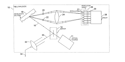
FIG. 2 is block diagram of an exemplary single-source
optical wavelength division multiplexer 10 in accordance
with the present invention, suitable for use in a variety
of optical applications. The multiplexer 10 includes an
optical source 11 which provides an optical pulse signal
12 on its output. The optical source 11 may be, for
example, a pulsed or a mode-locked laser. The optical
pulse signal may include a train of optical pulses, with
the optical pulses having a certain pulse shape. A
variety of different pulse shapes may be used, including,
for example, a Gaussian pulse shape or a secant-hyperbolic
pulse shape. The optical pulses in the exemplary optical
pulse signal are typically repeated at a particular pulse
repetition rate. The pulse repetition rate required for a
given application may vary widely, and may be, for
example, between about 100 MHz and 2.5 GHz. Other pulse
repetition rates, up to 350 GHz or more, could also be
used. The pulse duration may be varied to obtain a
- 12 -
frequency spectrum capable of providing a desired number
of channel signals. As explained further below, the
number of channels which the pulse frequency spectrum may
be separated into depends upon the width of the spectrum.
Although pulse durations in the sub-picosecond range are
preferred for many applications requiring a large number,
or a high density, of channel signals, pulse durations
longer than 1.0 picosecond may also be used.
The optical pulse signal passes over a beam pick-off
mirror 14. The beam pick-off mirror is arranged such that
an optical signal from source 11 passes unreflected over
an edge of the mirror, but an optical signal returning
toward the source 11 may be picked off by the mirror and
reflected in a direction away from the source. Use of the
pick-off mirror 14 minimizes optical signal loss. In
applications in which additional optical signal loss is
acceptable, a beam splitter could be used in place of
pick-off mirror 14. A portion 16 of the pulse signal 12
out of beam splitter 14 is incident on a wavelength
splitter 18 which divides the pulse signal spectrum into a
plurality of channel signals. The wavelength splitter may
be a diffraction grating or other suitable wavelength
splitter, such as a Dragone wavelength router. The
Dragone router is described in, for example, C. Dragone,
"An NxN Optical Multiplexer Using a Planar Arrangement of
Two Star Couplers," IEEE Photonics Technology Letters,
Vol. 3, No. 9, pp. 812-815, September 1991. The
individual channel signals, or portions of the pulse
signal spectrum, are reflected from the diffraction
grating 18. The paths traveled by two exemplary channel
signals 20, 22 are shown in FIG. 2. The channel signals
may then be separately processed in any manner required by
a particular application.
In the exemplary embodiment shown, the channel
signals are focused on a modulator array 26 by a lens 24,
- 13 -
and are separately processed by modulating each channel
signal incident on the modulator array 26 with, for
example, a data signal from an electronic circuit 28. The
modulator array 26 includes a plurality of individual
channel signal modulators 27, which may be reflection-mode
quantum well modulators. Other types of modulators,
including, for example, electro-optic or acousto-optic
modulators, could also be used. Each of the channel
signals is incident on one modulator 27 in the array 26.
One or more data signals are supplied from the circuit 28
along lines 29 to the modulators 27. The data signals on
the lines 29 may be high-speed electrical signals at data
rates of up to 2.5 Gbits/sec or higher, or other types of
digital or analog signals from circuit 28. The data
signals are generally time-varying signals, although
various constant signal levels may also be used as data
signals in a given application. However, maximum WDM
system data capacity is obtained by using data signals
which vary at the highest data rate supported by each
channel signal.
The data signals on the lines 29 are modulated onto
the various channel signals within modulator array 26.
The exemplary modulators 27 of array 26 operate in the
reflection mode. In a reflection-mode modulator, the
channel signal incident on each modulator 27 is modulated
by a data signal and then reflected out of the modulator
back toward the lens 24. The lens 24 focuses the various
channel signals onto diffraction grating 18, which
recombines the channel signals into a single WDM optical
signal. The WDM signal includes a number of separately
modulated channel signals, with each channel signal
typically including many longitudinal modes of the optical
pulse signal source. The WDM signal travels from the
diffraction grating 18 back toward the pick-off mirror 14,
where it is reflected and travels along path 30 toward
' -
- 14 -
lens 32. In order for the pick-off mirror 14 to reflect
the optical WDM signal returning from grating 18, while
the unmodulated optical pulse signal from source 11 passes
unreflected over the mirror, it may be necessary to tilt
the grating 18 or the array 26 such that the WDM signal
returns toward source 11 on path below that travelled by
the unmodulated pulse. Lens 32 focuses the reflected WDM
signal onto an optical transmission medium 34, which may
be free space, optical fiber, or different types of
waveguides, such as, for example, a polymer waveguide.
The multiplexer 10 of FIG. 2 therefore provides a multi-
channel optical WDM signal using only a single optical
source 11. The WDM signal out of lens 32 may be used in a
variety of optical applications, including optical
interconnections and optical communication networks.
In the exemplary embodiment of FIG. 2, a reflection-
mode modulator is used, and thus a single diffraction
grating 18 may serve as both a wavelength splitter and a
wavelength combiner. The modulated channel signals are
reflected back toward the grating 18 by the reflection-
mode modulator array 27, and the grating 18 then
recombines the modulated channel signals into a single
optical signal which may be propagated down an optical
fiber. As previously noted, other types of modulators,
including non-reflective modulators, may also be used.
With a non-reflective modulator, a separate wavelength
combiner may be used after the modulator array in order to
recombine the modulated channel signals of the optical WDM
signal.
In an optical interconnect application, it may be
desirable to connect the data signals from a first
circuit, such as circuit 28 in FIG. 2, to another circuit.
For example, the first circuit may contain a signal
generator which supplies timing signals to another
circuit. The circuits may be, for example, silicon or
2 ~
gallium arsenide electronic circuits operating at high
signal speeds. Prior art interconnection of high-speed
electronic circuits would typically rely upon direct
electrical interconnection using, for example, high-speed
coaxial cable. As previously mentioned, however, direct
electrical interconnection may also create a number of
problems, including high cost, inflexibility, ground
loops, cross-talk between the cables, reduced signal-to-
noise ratio and excessive power dissipation.
An exemplary embodiment of an optical interconnection
system using a single-source WDM 10 in accordance with the
present invention is shown in FIG. 3. As discussed in
connection with FIG. 2, the multiplexer 10 provides an
optical WDM signal to an optical transmission medium 34.
The optical source 11 may be synchronized to a signal,
such as a clock, from one of the circuits to be
interconnected, such as first circuit 28. The optical
transmission medium may be optical fiber or free space,
and is used to interconnect data signals from two or more
circuits. Optical fiber will be used as the transmission
medium 34 in this example. In FIG. 3, a lens 36 receives
the optical WDM signal from the optical fiber 34 and
focuses the WDM signal onto a second wavelength splitter
40. The second wavelength splitter may be, for example, a
diffraction grating or a Dragone wavelength router. In
the exemplary embodiment shown, a diffraction grating 40
is used as a wavelength splitter.
The diffraction grating 40 splits the WDM signal into
several channel signals with different longitudinal modes.
Two exemplary channel signals travel along the paths 41,
42. The channel signals on paths 41, 42 are focused via
lens 43 onto a detector array 44 which includes a
plurality of optical detectors 45. One of the modulated
channel signals of the optical WDM signal is incident upon
each optical detector. The detectors may be positive-
~<~,f~
- 16 -
intrinsic-negative (PIN) photodiodes, or other suitable
optical detectors. The detectors 45 demodulate each of
the incoming channel signals to, for example, recover the
data signals from first circuit 28. The demodulated data
signals may then be supplied to, for example, data signal
inputs on second circuit 46. A single optical source may
thus be used, in accordance with the present invention, to
interconnect two or more high-speed electronic circuits.
When interconnecting more than two circuits, optical
amplifiers may be needed to overcome signal loss due to
splitting or coupling the WDM signal to supply it to the
additional circuits.
Although the exemplary embodiment of FIG. 3
illustrates optical interconnection of data signals from a
first circuit to data signal inputs on a second circuit,
many other alternative arrangements will be apparent to
those skilled in the art. For example, data signals may
also be sent from the second circuit, and received in the
first circuit, by switching the modulators and detectors
of the circuits corresponding to particular WDM channels.
Since the modulators operate in reflection mode, an
unmodulated channel signal incident on a modulator placed
at a particular channel position in the detector array 44
could be modulated by a data signal from second circuit
46. The modulated channel signal could then travel back
through the lens 42, diffraction grating 40, lenses 36,
32, beam pick-off mirror 14, diffraction grating 18, and
lens 24, and be incident upon an element of array 26 in a
particular channel position. The modulator element in
array 26 could then be replaced with an optical detector,
such that the incident modulated channel signal may be
demodulated to supply the data signal from the second
circuit 46 to a desired point on the first circuit 28.
Alternatively, both modulators and detectors for each
channel signal could be included on each circuit, with an
- 17 -
optical switch for directing a particular channel signal
to either a modulator or a detector. As noted above, the
data signals from one circuit may be connected to several
different circuits by using a beam splitter or an optical
coupler at the output of multiplexer 10. The beam
splitter or coupler may be used to supply the optical WDM
signal to additional circuits or systems as required in a
given application. An amplifier could be included at the
beam splitter or coupler output, to offset optical signal
loss.
FIG. 4(a) is a block diagram of an exemplary optical
communication network 50 in which the single-source
optical WDM of the present invention may be used. The
optical communication network 50 includes a central office
52 which contains an optical wavelength division
multiplexer such as that described in conjunction with
FIG. 2 above. The network also includes a number of user
nodes 54 arranged in a ring configuration. The central
office 52 and the various user nodes 54 are interconnected
via optical fiber 56. Alternative network configurations
could also be used, including the star configuration shown
in FIG. 4(b). The optical WDM within the central office
52 includes an optical source, and may include an array of
reflection-mode modulators and a single diffraction
grating serving as both a wavelength splitter and a
wavelength combiner. The multiplexer within central
office 52 may therefore be, for example, the multiplexer
10 shown in FIG. 2. Other alternative multiplexer
embodiments may also be used within central office 52.
The central office 52 also includes other network
processing hardware, such as data signal switching
equipment.
The optical multiplexer within central office 52 may
output an optical pulse signal with a pulse duration of
about 1.0 picosecond to 100 femtoseconds or less. As
- 18 -
noted above, the pulse duration is related to the
bandwidth of the source output spectrum, and typically a
larger number of channel signals may be accommodated using
a pulse signal with a shorter pulse duration. The pulses
are repeated at a pulse repetition rate, which may be
equivalent to a fundamental data rate of the network.
Within the central office 52, the optical pulse signal
spectrum is divided into separate channel signals using a
diffraction grating or another suitable type of wavelength
splitter. Each channel signal may then be individually
modulated. The channel signals may be recombined within
the same diffraction grating if, for example, reflection-
mode modulators are used. A WDM optical signal is
therefore supplied from the single-source multiplexer
within the central office 52 to the individual user nodes
54 on the communication network. Within each user node
54, the individual channel signals of the WDM signal may
be selectively modulated or detected.
FIG. 5(a) is a block diagram of an exemplary user
node suitable for use as one of the nodes 54 in the
single-source optical WDM communication networks of FIGS.
4(a) and 4(b). The user node 54 receives a WDM signal
from the central office 52 on user node input 58. The WDM
signal on input 58 represents the recombined channel
signals of an optical pulse signal spectrum generated
within the multiplexer in central office 52. The
recombined channel signals of the WDM signal are again
separated in a wavelength splitter 60 in the user node 54.
The wavelength splitter 60 separates the incoming WDM
signal into a plurality of channel signals which are
spatially separated along paths 62. The channel signal of
each path 62 may then be individually detected or
modulated within an array 63. After modulation or
detection in the array 63, the channel signals travel
along paths 64 to a wavelength combiner 65 which
-- 19 --
recombines the channel signals into a single optical WDM
signal at its output 66. This signal then propagates
along the fiber 56 to another user node 54 or the central
office 52. In this manner, each of the user nodes may
transmit or receive information to or from the other user
nodes or the central office using the various channel
signals of the WDM signal. All of the channel signals
need not be modulated within the central office or
modulated and/or detected within any particular user node.
The number of channel signals used, and the arrangement of
modulator and detector elements within each array 63 of
the user nodes 54, may vary considerably from network to
network. It should be noted that the modulator and/or
detectors of array 63 do not operate in a reflection mode
in this embodiment. If reflection mode is used,
wavelength splitter 60 and wavelength combiner 65 could
be, for example, a single diffraction grating.
FIG. 5(b) is a block diagram of another exemplary
user node 67 suitable for use as one of the nodes 54 in
FIGS. 4(a) and 4(b). In this exemplary user node, only
certain channel signals are processed within the node.
Other channel signals are simply separated and recombined,
passing through the node without further processing. A
WDM signal is supplied to an input 68 of the user node 67
from the central office 52 or another user node. The WDM
signal is split into its channel signals in a wavelength
splitter 70. Several of the individual channel signals,
spatially separated and represented as travelling along
paths 72, are not modulated or detected within user node
67, but instead pass directly to a wavelength combiner 75.
One exemplary channel signal corresponding to one of the
signal paths 72 is modulated in a modulator 73. The
modulation or data signal used to modulate the particular
channel signal in modulator 73 may be any data or
information source associated with the particular user
-- 20 --
node 67. Wavelength combiner 75 recombines the various
channel signals into a WDM signal, and places the
recombined signal onto the optical fiber 56 via node
output 76. In this manner, data or other information
5 signals within each user node may be placed upon the
communication network, and transmitted to other nodes or
the central office, via one of the channel signals of the
WDM s ignal.
A different channel signal corresponding to another
10 signal path 72 within exemplary user node 67 is detected
in an optical detector 74. The modulated channel signal
is also recombined with the other channel signals and
placed back on the network for transmission to other nodes
or the central office via output 76 of the node 67. The
15 user node 67 can thus be supplied with data or other
information signals from the other nodes or the central
office, via one of the channel signals of the WDM signal.
It should be emphasized that the arrangement of modulators
and detectors in FIG. 5(b) is exemplary only, and
20 different numbers and arrangements of channel signals may
be modulated, detected, processed or simply passed through
the node unprocessed, as required in a given network
application.
In the above single-source WDM communication network,
25 the optical pulse signal source is located at the
network's central office. Because each channel signal
represents an available network channel, a large number of
channels are available within the network. In addition,
since each channel may independently handle a high-speed
30 electronic data signal, the electronic switching speed
requirements of the central office are significantly
reduced. The network switching may be accomplished
electronically in the central office at the lower data
signal switching rates, while the multiplexing of channel
35 signals multiplies overall network capacity by the number
7 ~ 5 ~
-
- 21 -
of channel signals used. For example, if an optical pulse
signal with a duration of about 100 femtoseconds is used,
up to 250 or more different channel signals may be
generated from the pulse spectrum. By using 250 WDM
channel signals, each carrying data at a 100 Mbits/sec
data rate, the total data transmission capacity of the
network is 25 Gbits/sec. The central office, however,
need only operate at the data signal switching speed of
100 Mbits/sec. A total capacity of 25 Gbits/sec is high
for a network with a central office operating at such a
moderate switching speed.
In existing WDM systems, channel misalignment and
fiber dispersion are serious problems. As mentioned
above, present techniques for addressing these problems
include active stabilization of the many individual
optical sources at both the transmitter and the receiver,
and using sections of fiber with an offsetting dispersion
characteristic in the fiber transmission path. The
techniques are generally inflexible and expensive to
implement. The single-source optical WDM of the present
invention maintains a fixed phase relationship between
channel signals, which permits the use of inexpensive,
accurate and flexible alignment and compensation
techniques. The phase relationship between channel
signals in the present invention is fixed because each
channel signal is composed of longitudinal modes of the
same optical signal source.
FIG. 6 is a block diagram of an exemplary user node
80 in a high-density single-source optical WDM network,
with dispersion compensation and channel alignment
capability in accordance with the present invention. An
optical WDM signal arriving on user node input 81 is
reflected off a beam pick-off mirror 82 toward a
diffraction grating 83. A beam splitter could be used in
place of mirror 82, but would generally result in greater
- 22 -
optical signal loss. The diffraction grating 83 in user
node 80 serves, in this embodiment, as both a wavelength
splitter and a wavelength combiner. The beam pick-off
mirror 82 is used to reflect optical WDM signals both into
and out of the user node 80. The diffraction grating 83
separates the incoming optical WDM signal into its channel
signals. The individual channel signals are spatially
separated by the grating 83 and are incident on a lens 84,
which focuses the spatially separated channel signals onto
the appropriate modulator or detector in an array 85. The
array 85 in the embodiment of FIG. 6 is an array of
reflection-mode modulators 86. The diffraction grating 83
and the modulator array 85 are spaced apart by a distance
Dl + D2 in a direction X, the importance of which will be
discussed below. The diffraction grating 83 may serve to
separate the incoming optical signal pulse spectrum into
various channel signals, as well as to recombine these
channel signals after they are individually modulated
within the modulator array 85. It should be noted that
although the embodiment shown includes an array of
modulators, the array could include modulators, detectors,
other processing elements, or simply a reflector, at any
or all of the array element positions. The beam pick-off
mirror 82 reflects the recombined WDM optical signal to
the user node output, also designated by reference numeral
81. In this particular embodiment, reflection-mode
modulators are used and the user node input and output may
therefore be the same.
By tilting grating 83 or array 85 slightly, the
recombined WDM signal may be made to pass unreflected over
the pick-off mirror 82 to a lens 88. The lens 88 focuses
the optical WDM signal onto a nonlinear crystal 90, which
generates optical signal harmonics in response to an
incident optical signal. Other nonlinear devices,
including optical four-photon mixers, semiconductor
-
- 23 -
amplifiers, and lengths of dispersion-shifted fiber, may
also be used to generate optical signal harmonics. A
harmonic detector 92 provides a measure of the power level
of a particular harmonic of the incident optical signal.
In the exemplary embodiment shown, the harmonic detector
92 is preferably a second harmonic detector.
The power level of certain harmonics generated by the
nonlinear crystal 90 indicate various characteristics of
the incident optical signal. For example, if a short
optical pulse signal is used to generate a single-source
optical WDM signal, the characteristics of the recombined
pulse signal are indicated by the amount of power at the
pulse signal second harmonic. In general, a pulse signal
which has sharp edges and is concentrated within a short
duration of time will have g-eater power in its even
harmonics than a signal whic:l is spread in time by, for
example, fiber dispersion. Of the even harmonics, the
second harmonic will generally have higher power levels
than the other even harmonics of the signal, such as the
fourth and sixth harmonics. Although any of the harmonics
of the incident optical signal could be used to indicate
the quality of the arriving optical signal, the even
harmonics, and in particular the second harmonic, provide
a convenient and accurate signal quality measurement in a
wide variety of applications.
In accordance with the present invention, an optical
pulse signal spectrum is split into N different
components, each of which may represent a distinct channel
signal. The optical source delivers the pulses of the
pulse signal at a particular repetition rate, on the order
of the system or network data rate. For each of the
pulses, the data modulated onto the N individual channel
signals may be represented as a data word of length N
associated with a particular pulse in the optical pulse
signal. As mentioned above, once the pulse is modulated
- 24 -
by a word of length N, the individual pulses of the
optical pulse signals are spread out in time such that the
pulse intensity at any one point in time is considerably
reduced. This effect has been noted in the context of
code-division multiple access (CDMA) communication with
optical pulse signals. See J. Salehi, et al., "Coherent
Ultrashort Light Pulse Code-Division Multiple Access
Communication Systems", Journal of Lightwave Technology,
Vol. 8, No. 3, March 1990. When the channel signals of
the WDM optical signal are modulated, the amount of second
harmonic power generated by the nonlinear crystal will be
relatively small. When each of the channel signals are
unmodulated, or modulated with a constant high level, the
optical pulse signal energy is concentrated within the
pulse duration, and the second harmonic power will be
relatively high.
Dispersion compensation of the single-source WDM
optical signal may be performed as follows. During the
normal operation of, for example, an optical network, the
optical pulse signals are spread in time as a result of
the time-varying data signals modulated onto the channel
signals of the pulse. Fiber dispersion introduces
additional time spreading as the signal propagates down
the fiber. The amount of time spreading is a function of
a variety of factors, including the length of fiber, its
dispersion characteristic, and the channel signal
wavelengths. At certain intervals in normal network
operation, the dispersion efi~ects may be isolated by
modulating a constant high l-~vel on each channel signal,
such that any time spreading effects due to channel signal
modulation are removed. In ~ffect, modulating a constant
high level on each channel signal leaves the channel
signals unmodulated, such that the original pulse shape is
maintained. As the pulse propagates down the fiber,
however, dispersion will continue to introduce time
' -
- 25 -
spreading of the pulse. Most or all of the pulse time
spreading will therefore be due to dispersion, rather than
a combination of dispersion and channel signal modulation
effects.
S During the intervals in which dispersion effects on
the optical pulse are isolated as described above, an
adjustment may be made to the positions of the modulator
array 85 or the grating 83 relative to the lens 84. This
position adjustment compensates for the dispersion-induced
time spreading of the optical pulse. The positions are
adjusted in a direction X which is substantially parallel
to the direction of propagation along the channel signal
path 93 at a point where the channel signals are incident
on array 85. The effect of relative grating position on
dispersion compensation is discussed in 0. Martinez, "3000
Times Grating Compressor with Positive Group Velocity
Dispersion: Application to Fiber Compensation in 1.3-1.6
~m Region", IEEE Journal of Quantum Electronics, Vol. 23,
No. 1, January 1987.
In the present invention, the distance Dl between the
modulator array 85 and the lens 84, or the distance D2
between the diffraction grating 83 and the lens 84, may be
adjusted to provide dispersion compensation.
Alternatively, the distance Dl + D2 between the modulator
array 85 and the diffraction grating 83 may be adjusted,
with the position of the lens 84 remaining the same. As
another alternative, the position of the lens 84 could be
adjusted while the positions of the array 85 and the
grating 83 remain unchanged. As mentioned above, the
position adjustment should be made while the optical pulse
signal is unmodulated, or modulated by a constant logic
high level, such that the ti~e spreading effects of
dispersion are isolated from the time spreading effects of
modulation. In general, several pulses of the optical
pulse signal may have to be modulated with a constant high
- 26 ~
logic level in order to provide sufficient time to make
position adjustments while observing second harmonic
signal power in harmonic detector 92. The significance of
the logic high level is that, in amplitude-shift keyed
modulation techniques, it generally corresponds to a
maximum carrier signal power level, such that a carrier
signal with a constant logic high level modulation is
substantially equivalent to an unmodulated carrier signal.
When other modulation schemes are used, the modulation
signal levels could be similarly adjusted to provide the
substantial equivalent of an unmodulated carrier signal.
The position of the grating 83, array 85 or lens 84
is adjusted in direction X, as described above, until a
maximum second harmonic signal power level is detected in
second harmonic detector 92. As previously noted, a
maximum second harmonic signal power typically corresponds
to a minimum amount of pulse time-spreading. When maximum
second harmonic power is observed, therefore, the
dispersion has been optimally compensated, and a narrower,
sharper-edged pulse is produced within the user node 80.
After the appropriate adjustment is made and maximum
second harmonic signal power is obtained, the various
channel signals may then again be modulated by time-
varying data signals, as in normal network operation. The
dispersion compensation position adjustments could be
repeated at regular intervals, such as after transmission
of a predetermined number of data packets, to properly
compensate for time-varying dispersion effects.
The exemplary user node 80 in FIG. 6 also includes
channel alignment capability in accordance with the
present invention. As in the dispersion compensation
technique described above, a certain time interval is
allocated for adjustment of relative positions of the
grating 83, lens 84, or array 85 while the channel signals
are modulated in a predetermined manner. For channel
- 27 -
alignment, the N channel signals are modulated with a
predetermined pseudo-random code of length N, with one bit
of the code modulated onto each of the N channel signals.
The same predetermined pseudo-random code is supplied to
the corresponding modulators 86 within the array 85.
During the interval in which the optical pulse signal and
the modulator array are modulated by the same pseudo-
random code, the second harmonic power level detected in
harmonic detector 90 is observed. In general, an optical
WDM signal with its channel signals modulated by the bits
of a pseudo-random code will be spread in time, just as a
WDM signal with its channel signals modulated by randomly-
varying data signals is spread in time. There will
therefore be very little second harmonic power when the
optical signal is spread by the pseudo-random code.
However, when the pseudo-random code modulated on the
channel signals of the incoming WDM signal matches the
modulation placed on the channel signals within the
modulator array, the original unmodulated optical pulse
signal is reproduced, since the modulation of each channel
signal is in effect cancelled out. The reproduced
unmodulated optical pulse signal has significant power in
its second harmonic, which may be detected by the second
harmonic detector 92. The second harmonic power level can
thus be used to indicate a match, or an alignment, between
channel signal wavelengths at the optical source and
channel signal wavelengths at the user node 80.
The alignment technique of the present invention
ensures that a channel signal corresponding to one channel
position at the transmitter does not drift to another
channel position at the receiver. During the time
interval in which the pseudo-random code is modulated onto
the channel signals, the position of modulator array 85 is
adjusted in a direction Y substantially perpendicular to
the propagation direction of the channel signal path 93 at
~
- 28 -
a point where the channel signals are incident on array
85. In this manner, the individual modulators 86 within
array 85 may be made to modulate different channel signals
with a particular bit of the pseudo-random sequence. When
the bits modulated on the channel signals by modulators 87
in the user node 80 match the bits already modulated on
those signals in the transmitter, the original pulse is
reconstructed and the second harmonic power measured in
the detector 92 will be maximized. If the channel signal
wavelengths had drifted such that the channels were each
offset by, for example, one channel position at the
receiver from their channel positions at the transmitter,
the position of array 85 could be adjusted in direction Y
by a distance corresponding to one modulator element, or
channel position, in which case the original optical pulse
again may be properly recombined and detected. Without
the adjustment, the channel signals would have been
misaligned and the modulated data signals would have been
received on the wrong receiver channels. As an
alternative, the alignment adjustment could be provided by
adjusting the position of grating 83 in direction Y.
The dispersion compensation and channel alignment
techniques described above may be implemented using a
closed-loop automatic control system, with feed~ack from
the second harmonic detector 92 driving a motor or other
adjustment mechanism which varies the position of one or
more of the grating 83, lens 84 or array 85 in direction X
or direction Y until second harmonic power is maximized.
The control system could also control the modulation
applied to the channel signals at the central office and
within the node, such that an effectively unmodulated
optical pulse is incident on the nonlinear crystal 90
during the compensation adjustment, and a pseudo-random
code-modulated pulse is used during channel alignment
adjustment. After a particular position adjustment is
- 29 -
complete, the control system would again permit data
signals to modulate the channel signals as in normal
operation.
The dispersion compensation and channel alignment
techniques are described above in the context of a
particular embodiment of a single-source high-density
wavelength division multiplexer in an optical network user
node, which uses a pulsed optical signal, an array of
modulators, and a second harmonic detector. The
compensation and alignment techniques may also be used in
other optical applications, such as interconnects, and
with other types of optical pulse signals. The array 85
may include detectors, reflectors, and other processing
elements in addition to or instead of the modulators 87,
and may be operated in a non-reflection mode, in
alternative embodiments. Furthermore, other harmonics or
signal characteristics of the optical signal may be
detected to indicate proper compensation or alignment.
Although the foregoing detailed description has
described the present invention primarily in terms of
particular applications of single-source high-density
WDMs, it should be understood that the embodiments
discussed are exemplary only. Many variations may be made
in the arrangements shown, including the type of optical
pulse signal and signal source used, the number of channel
signals, the type of wavelength splitters and combiners,
and the modulating, demodulating or other signal
processing operations performed on the individual channel
signals. These and other alternatives and variations will
be readily apparent to those skilled in the art, and the
present invention is therefore limited only by the
appended claims.