Note: Descriptions are shown in the official language in which they were submitted.
CA 02132629 1998-06-17
Image Cell in Particular for an Image-Recorder Chip
D e s c r i p t i o n
Technical Field
The present invention relates to an image cell, in
particular, for an image-recorder chip having a
multiplicity of image cells disposed in the form of a
two-dimensional array and having a readout logic, for the
projection of high input signal dynamics onto reduced
output signal dynamics.
Natural scenes have irradiation intensity dynamics of, in
some instances, more than 1,000,000:1. In order to be
able to image scenes of this type simultaneously with an
image-recording system, each element of the signal
processing chain, i.e. the sensor element, the readout
logic, as well as, if need be, A/D converters connected
thereafter for reading the image into an image-processing
system, would have to have a dynamic range of 120 dB. A
dynamic range of this type can be achieved with
individual components, such as special semiconductor
diodes or discrete A/D converters, however, elements
which have a dynamic range of 120 dB are not suited for
integration into a digital CMOS process. On the other
hand, almost any dynamics can be achieved on the digital
"side", i.e. in a subsequently connected image-processing
unit with the respective hardware complexity.
CA 02132629 1998-06-17
State of the Art
An image-recorder chip whose light-sensitive elements are
photo diodes or MOS transistors whose generated signals
are all converted logarithmically has been proposed in US
Patent No. 4,973,833. A charge coupled device (CCD) is
utilized for storage and transfer of the signals from the
light-sensitive elements.
The image-recorder chip known from US Patent No.
4,973,833, however, has the drawback that the
input signal dynamics cannot be controlled, but
rather in the case of the image recorder described in US
Patent No. 4,973,833, the input signal dynamics are defined
"logarithmically". Furthermore, direct and nondestructive
readout of the image data is not possible.
EP 0 390 205 A2 describes an electrical circuit that is
distinguished by high amplification during the conversion of
the electrical charge into voltage. This circuit is
predominantly employed for charge coupled devices (CCDs). In
this circuit described in EP 0 390 205 A2, there is also no
possibility of controlling the compression of the input
signal. The amplifier circuit according to EP 0 390 205 A2
permits high amplification for small charges, however, cannot
control the amplification factor and quickly reaches its
limits with high charges.
US Patent No. 4,473,836 proposes an image-recorder chip in
which a MOS field-effect transistor is the light-sensitive
element. The gate electrode of the MOS field-effect
transistor is electrically connected to a floating
photosensitive diffusion area, yielding an image cell that
projects high input signal dynamics onto reduced output
signal dynamics. This cell permits further signal processing
with conventional circuits produced in the same MOS process,
CA 02132629 1998-06-17
processing with conventional circuits produced in the
same MOS process, because greatly reduced dynamic demands
are made on these components.
The image-recorder chip known from US Patent No.
4,473,836 has, however, a number of drawbacks:
For one thing, the projection of the input signal
dynamics onto the output signal dynamics occurs only
approximately logarithmically, with the exact course of
the characteristic line being greatly dependent on the
fabrication parameters. The initially logarithmic
characteristic line changes into a "root characteristic
line". Moreover, supply voltages are needed that are
incompatible with the supply voltages of digital CMOS-
VLSI circuits.
Furthermore, the known image recorders with initially
logarithmic signal compression are not manufactured for
array arrangement or have to be made using special
processes due to the intolerance to fluctuations of the
process parameters.
Description of the Invention
The object of the present invention is to provide an
image cell, in particular, for an image sensor, which
projects high input signal dynamics with a characteristic
line which can be selected within a specific range and,
in particular, logarithmically onto output signal
dynamics.
It should be possible to fabricate this image cell and
therefore a respective image sensor with conventional
CMOS technology, to integrate it with digital circuit
CA 02132629 1998-06-17
components as well as to operate it with a single supply
voltage, which is compatible with conventional digital
CMOS circuits.
Furthermore, the invented image sensor should permit
realization of low-noise signal amplification as well as
suppression of cyclical crosstalk during readout. In
addition, it should be possible to read out the picture
elements with a high pixel repeat rate (>>50Hz as is
usual in HDTV applications) and to the greatest extent
with random access.
A solution according to the present invention to this
object is set forth in the claims.
An element of the present invention is that for
projection of high input signal dynamics onto reduced
output signal dynamics the light-sensitive element of
each image cell is connected to the one electrode of a
first MOS transistor and to the gate of a second MOS
transistor. The other electrode of the first MOS
transistor is connected to a pole of a supply voltage
source.
It is preferable if an electrode of the first MOS
transistor is the source electrode and the other
electrode the drain electrode (claim 2).
The invented image cell has a characteristic line
"illumination intensity, respectively irradiation
intensity/output signal" which can be set within a
specific range, in particular, by means of the
application of a suitable control voltage to the gate
electrode of the first MOS transistor. This control
CA 02132629 1998-06-17
voltage permits controlling the compression of the input
signal dynamics.
In particular, if according to claim 4 the drain
electrode and the gate of the first MOS transistor are
short-circuited and applied to a fixed potential, an
exact logarithmic characteristic output line permitting
a radiometrically unequivocal evaluation of the image
data, is yielded over a range of more than seven decades.
The invented image cell has, in addition, a number of
other advantages:
For instance, the image cell and thus the invented image
sensor can be produced with almost any process, such as
growing cell cultures as sensor elements on a passivated
chip which serves as a "junction" for the derivation of
potentials only via an electrode that can be contacted at
the top.
Coupling Schottky diodes as sensor elements is also
possible, in particular, for the infrared range.
Moreover, diodes that are sensitive to electro-magnetic
radiation (in particular light-sensitive diodes) may be
considered as sensor elements.
In another preferred embodiment preferred for image
sensors for the visible spectral range, the light-
sensitive element is the one electrode of the first MOS
transistor (claim 3).
Especially in this case, the invented image sensor may be
realized in a standard CMOS process for digital circuits,
such as a process with two metal layers and a polysilicon
CA 02132629 1998-06-17
-- 6
layer, as well as in a 2~m n- or p-trough process or a
1.2~m p- or n-trough process (and even smaller channel
widths). The invented image sensor may then also be
operated with standard CMOS supply levels.
Due to the invented arrangement, the image data can be
read out without destruction of the image data.
Therefore the readout logic may be designed in such a
manner that it permits random access to the individual
image cells (claim 9). This is especially advantageous
if the recorded image is to be processed further in an
image-processing device, because it often suffices to
just read out a part of the image cells in order to check
a scene. In this case, it is preferred if according to
claim 10 a subsequently connected image-processing device
controls the readout of randomly accessible cells via a
bus and the readout logic.
Furthermore, it is preferred if each individual image
cell, respectively each sensor element has suitable
drivers which permit triggering a parasitic capacitative
load, e.g. a reading line. These drivers may, however,
only be activated for access in order to save energy and
not heat up the surroundings of the sensors, respectively
to reduce thermal noise.
In the further improvement described in claim 5, the
second MOS-transistor is provided as a source follower
and being part of the readout amplifier for this purposeO
In this case, it is preferred if the driver is designed
two-stage (claim 7).
This yields a quick answering time on the (random)
addressing without the sensor element being charged with
CA 02132629 1998-06-17
a high input impedance. A suitable zero signal current
during the first stage is forced by means of the circuit
in such a manner that the level control of the second
power stage ensues with adequate velocity. Compared to
the conventional sensor structures, in this way arrays
with considerably less current consumption can be built.
Usual values are 100 mW for a 4096 pixel size array
including decoder.
Moreover, even in the "worst case", i.e., an irradiation
intensity of <l~W/cm2 a pixel repeat rate of lkHz is
possible.
The further improvement described in claim 8, in which
the metal layer covering the areas that are not supposed
to be light sensitive is utilized as a supply line for
the circuit, not only simplifies the fabrication process
but also improves the voltage supply.
Brief Description of the Drawing
The present invention is described in the following using
preferred embodiments with reference to the drawing, to
which expressly is referred with regard to the disclosure
of any invented details not explained more closely
herein, by way of example without the intention of
limiting the scope or spirit of the overall inventive
idea. Shown are in:
Fig~ 1 a section of an invented image-recorder array,
FigO 2 a cross-section of an image cell,
Fig. 3 measurement results obtained using this preferred
embodiment,
CA 02132629 1998-06-17
.
Figs. 4a and 4b a comparison of an invented sensor with
a conventional sensor with "linear sensitivity".
Description of Preferred Embodiments
Fig. 1 depicts a section of 2*3 image cells, respectively
sensor elements 11...13, 21..23 of an image-recorder
array. Shown in the lower part of Fig. 1 are analogous
multiplexers 31, 32 and 33 with a digital input.
In the depicted preferred embodiment, each image cell,
respectively each sensor element 11..23 is composed of
six MOS transistors M1, M2, M2a, M3, M3a and M4, which by
way of illustration may be p-channel enhancement
transistors. The light-sensitive element of each image
cell 11.. 23 is the source electrode of the first MOS
transistor M1, which is connected to the gate of the
second MOS transistor M2, which is connected as a source
follower. The drain electrode of the first MOS
transistor M1 is connected to the one pole Vss of the
voltage supply source.
The source follower M2 is utilized for impedance
conversion and is integrated, with consideration to good
high-frequency behaviour, immediately adjacent to the
sensor element, in the depicted preferred embodiment thus
transistor M1.
The MOS transistor M3 serves as a "load" element, i.e.
the load for the source follower M2.
Another MOS transistor M3a, also connected as a source
follower, composes the second amplifier stage. MOS
transistor M2a is utilized as the load for this amplifier
stage, whereas output transistor M4 is connected as a
CA 02132629 1998-06-17
power transistor. The MOS transistors M2a and M4 are
switched through only during a readout procedure, in
which the control line designated "row_sel" for the
selection of the row to be read out is actively applied
to a low potential, so that they only draw power during
the readout procedure.
The selection of the column to be read out (col_sel)
occurs via the analogous multiplexers 31..33, which are
triggered via a digital input signal (col_sel). For the
exact design of this circuit component, Fig. 1 is
explicitly referred to.
The depicted circuit permits low noise amplification
directly at the sensor element and adaption of the
desired array area, respectively the desired read-out
periods.
In the depicted circuit in Fig. 1, it is preferred if all
the circuit components except for the photo-active source
electrode of the MOS transistor are covered by an
aluminium screen which simultaneously is utilized to
supply the chip electrically (Vss) and to stabilize the
voltage supply (utilization as filter capacitor!),
therefore permitting greater integration density.
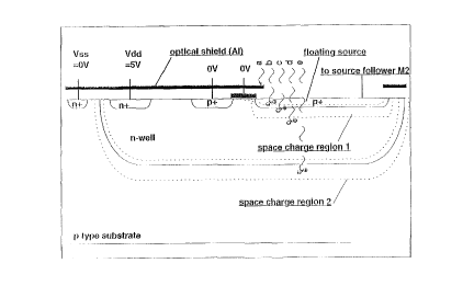
Fig. 2 depicts a possible realization of an image cell
11 .23. The transistors M1 to M6 are p-channel
enhancement transistors in an n-trough, which is applied
to a positive supply potential Vdd (5V), whereas the
substrate beneath it is contacted to a negative supply
potential Vss (OV).
CA 02132629 1998-06-17
- 10
Accordingly, an image cell exclusively of n-channel
enhancement transistors in a p-trough or CMOS transistors
in several troughs is, of course, also realizable but at
the expense of the space factor.
As already mentioned, the actual photo-active element is
the "floating source" of the MOS transistor M1, because
the remaining circuit is covered by the aluminum screen
A1 which prevents radiation particles impinging on it
(case a in Fig. 2) from generating charge carriers in the
semiconducting material.
The "floating source" collects "holes" which are
generated by the action of the light in the n-trough and
reach the space charge region 1 by means of diffusion or
drift current (the latter only to a negligible extent) or
are generated directly in the space charge region 1
(cases c and d in Fig. 2). Charges generated in the
layers close to the surface of the source electrode (case
b) are for the most part caught in "surface traps" and
therefore hardly contribute to the generated photo
current. Charges generated in the space charge region 2
can be eliminated via the trough, respectively the
substrate. Only the charge carriers that are collected
in the space charge region of the source electrode and
are directly proportional to the absorbed light energy
contribute to increasing the potential but do not lead to
forming an inversion layer in the channel, because the
source potential always stays under the threshold voltage
as 5V is applied to the n-trough.
Contrary to conventional, integrated photodetectors, in
the image cells designed according to the present
invention, the charges are eliminated by the channel in
CA 02l32629 l998-06-l7
the form of "subthreshold" currents; i.e. if the
eliminating transistor is correctly dimensioned,
saturation cannot set in even if irradiation with visible
light occurs in the <lOW/cm2 range.
The "subthreshold" current, which ultimately influences
the source potential, may be calculated from the
following equations:
IST = (KlcB)*(kT/q)2*e[q(~ss-2~F)/kT]*(l-e[(-qvDs)/kT]) (1)
CB = (K2/[2(~Ss-VBs)])l/2 (2)
~SS = VGS-vFB-vo[1+2(vGs-vvB-vBs)]
with Kl = ~neffW/L
~n_eff = effective electron
mobility
K2 = qKs~oNB with
KS = dielectric constant of Si
NB = net concentration of dopant
CB = capacity of the depletion region
( F/cm2 )
k = Boltzmann's constant
T = Kelvin temperature
q = elementary charge
~F2 = Fermi potential
~sS = surface potential of the source
VO = qKS~oNB/(co)2 with
CO = area normed oxide capacity
(F/cm )
VFB = flat band voltage
VDs = drain source voltage
VBs = bulk source voltage
VGs = gate source voltage
CA 02l32629 l998-06-l7
- 12 -
The second exponential factor in equation (1) may be
ignored for VDs > kT/q.
Due to the circuit of the sensor element depicted in Fig.
1, VGS-VBs is independent of Vs; i.e., a constant.
Therefore ~sS in equation (3) depends directly on VGs and
results in another constant if utilized in equation (2) .
Renewed use in equation (1) shows that there is a purely
exponential dependency of Vs for IST; i.e., that the
photocurrent is proportional to the logarithm of the
source voltage and therefore proportional to the
irradiated light power. In the hitherto known similar
structures (1), the connection of the source to the gate
results in additional square-root dependency in equations
(2) and (3).
Fig. 3 depicts the dependency of the output voltage in mV
as the function of the irradiation intensity, with it
being plotted on the abscissa in arbitrary units of loX.
Fig. 3 shows that an exact lin-log conversion occurs over
a range of seven decades.
Fig. 4a shows in the top part the output signal of an
invented image cell as the function of the illumination
intensity plotted on the abscissa. The intensity of the
light incident on the image cell doubles with each step
in x-direction. The corresponding output signal o~ the
image cell having the logarithmic characteristic line is
plotted on the y-axis in arbitrary units.
Fig. 4b shows the corresponding illustrations for a
conventional image cell having a "linear sensitivity".
CA 02l32629 l998-06-l7
- 13 -
Plotted in the bottom part of Figs. 4a and 4b is the
resolvable contrast for the respective image cells if an
A/D conversion occurs using an 8-bit A/D converter. With
the invented image cell, the resolvable contrast is
independent of the illumination intensity constant,
whereas with conventional image cells it sinks with
increasing intensity and recedes to lower values.
The invented image cells, respectively sensor elements
permit exact logarithmic compression of light signals and
are suitable, therefore in particular, for the projection
of highly dynamic light signals. The integration of
sensor elements and readout amplifiers in an image cell
that can be processed in standard CMOS processes
(suitable for p-troughs as well as n-troughs) qualifies
this image sensor cell for building XY-image sensors with
integrated digital image processing.
However, the invented image cell is also suitable as a
"stand alone element", by way of illustration as a light-
sensitive element for use in repeaters for lightwave
conductors.