Note: Descriptions are shown in the official language in which they were submitted.
wo 93/19380 2 1 3 2 7 ~ I Pcr/usg3/02560
MAGNETIC IN'rERFEROMETER
BACXGROUND OF q!EIE INVENq!ION
~ield of the Invention
The pre~ent invention relates to a device for the
inspection and quality control of wire rope and cables. The
device is adapted to concentrically surround a portion of a
wire rope or cable to be tested. The device induces a magnetic
field in the wire rope or cable and senses any deviation in the -
magnetic field indicating an anomaly in the wire rope or cable.
Descri~tion of the Prior Art
Polish Patent No. 45,862 discloses an induction sensor of
a measuring head for the inspection of cables. The induction
sensor has a two-part frame with cutouts of different diameter
in which are located two bifilar coils connected in series and
arr~nged concentrically with respect to the axis of the sensor
and sep~rately in the upper and lower parts of the frame.
Polish Patent No. 122,500 discloses two devices for the
inspection ~nd quality control of steel cables. According to
eaah device a cable is magnetized by a magnetic field set up by
a circuit which includes permanent magnets, the steel cable and
polQ pieces which are attached to the permanent magnets and
include sliding guides which cont~ct the steel cable.
The devices disclosed in Polish Patent No. 122,500 have
several serious drawbacks. First, the inclusion of the pole
pieces and sliding guides, some of which are necessarily made
of ferrous material, makes the devices quite large and quite
heavy. In addition, due to the large size of these devices,
they require that the cable undergoing testing be contacted by
the sliding guides which are subject to failure due to
frictional erosion after a certain period of use.
SUMMARY OF ~HE INVENTION
The magnetic interferometer of the present invention
avoids the above-mentioned disadvantages which are
characteristic of the prior art. The magnetic interferometer
of the present invention provides a means for performing
nondestructive magnetic induction testing and inspection of
wire rope and cable.
WO93/1s~0 PCT/US93/02~
2132717
-- 2 --
The magnetic interferometer of the present invention is
adapted to concentrically ~urround a wire rope or cable to be
tested and comprises means for inducing a magnetic field in
wire rope or cable and means for detecting flux changes in the
induced magnetic field. A change in the flux of the induced
magnetic field indicates that there is an anomaly in the
cross-sectional profile of the wire rope or cable undergoing
testing.
In a preferred embodiment of the present invention, the
means for inducing a magnetic field comprises a pair of magnet
housings, each of which is provided with a plurality of
rectangular permanent magnet~ arranged to form a segmented
cylinder spaced apart from and surrounding the wire rope or
cable. Corresponding magnets of each housing are paired in
alignment longitudinally to create a magnetic circuit having
lines of magnetic flux passing axially through and parallel to
the wire rope or cable.
In this preferred embodiment, the means for detecting flux
changes in the induced magnetic field comprises a sensing
device which include~ longitudinally spaced inner and outer
sensing arrays, each of which includes sensing elements
circumscribing the wire rope or cable which are positioned
perpendicular to the axis of the wire rope or cable. The
elements are spaced apart from the wire rope or cable with the
elements of the inner sensing array positioned closer to the
wire rope or cable than the elements of the outer sensing
array. The elements of the inner sensing array are aligned to
be in the same longitudinal planes as corresponding magnet
pairs. The elements of the outer sensing array are
rotationally displaced relative to the inner sensing array so
as to be aligned in longitudinal planes midway between
corresponding magnet pairs. Bifilar, helical windings encircle
each of the elements. The windings for each of the inner and
outer arrays are connected re~pectively in series. An
electromotive force is induced in the windings in response to
magnetic flux changes in proximity thereto thus producing a
signal which may be processed and which is indicative of the
condition of the wire rope or cable~
. --` WO 93/19380 2 1 3 2 7 1 7 PCI/US93/02560
BRIEF DESCRIPTION OF THE DRAWINGS
In describing the invention, reference will be made to the
accompanying drawings, in which:
FIG. 1 is a perspective view of the magnetic
interferometer o~ the present invention;
FIG. 2 is a section ta~en along the line 2-2 of FIG. l;
FIG. 3 is a section taken along the line 3-3 of FIG. 1;
FIG. 4 is an exploded view of the magnetic interferometer
~hown in FIG. 1 with portions omitted for clarity;
;~ FIG. 5 is a longitudinal section of the magnetic
interferometer of the present invention with portions omitted
for clarity;
FIG. 6 is a section taken along line 6-6 of FIG. 5;
FIG. 7 is a functional block diagram of the digital signal
processor of the present invention;
FIG. 8 is a flow chart illustrating the program logic for
the initialization of the microcontroller;
~: FIG. 9 i~ a flow ch~rt illustr~t~ng the program logic for~ the initialization of the header ~ile;
:~ FIG. ~O is a flow chart illustrating the program logic for
the ~cqui8ition and tran8fer of d~ta;
FIG. 11 is a flow chart illustrating the program logic for
~` the ¢alibration of the interferometer;
FIG. 12 is a flow chart illustrating the program logic for
the interrogation and reset of the interferometer's internal
clock;
FIG. 13 is a flow chart illustrating the program logic to
print and display the acquired data;
FIG. 14 is a perspective view of an alternative embodiment
of the present invention;
FIG. 15 is a section taken along the line 15-15 of FIG. 14;
FIG. 16 is a section taken along the line 16-16 of
FIG. 15; and
FIG. 17 is a section taken along line 17-17 of FIG. 16.
DETAILED DESCRIPTION OF THE PREFERRED EMBODIMENTS
Referring now to the drawings, and in particular to
FIG. 1, a prèferred embodiment of the magnetic interferometer
of the present invention is generally indicated at 10. The
. ; .
wos3/l938o PCT/US93/02~
2132717
-- 4 --
magnetic interferometer 10 is adapted to concentrically
surround a ferromagnetic metal wire rope or cable 12 to be
tested for anomalies in its cross-sectional proiile. As used
herein, the term cable shall refer to any type o~ rope, wire,
pipe, tubing, cable, or the like, made of ferromagnetic
material.
The magnetic interferometer 10 includes a first magnet
housing 14, a second magnet housing 16 and a sensing device 18
disposed between the first magnet housing 14 and the second
magnet housing 16. The cable 12 is centrally located within a
central bore 20 (see FIGS. 2 and 3) which runs the entire
length of the magnetic interferometer 10 from the first magnet
housing 14, through the sensing device 18, and through the
second m~gnet housing 16.
In one embodiment of the present invention, and referring
also to FIG. 4, the first magnet housing 14 includes an outer
housing 22. The outer housing 22 is a sixteen-sided
cylindrical mQmber having a central cavity. It will be
recogniz~d by those skilled in the art that the outer housing
22 is not r~quired to have sixteen s~des, but may have any even
number of sides greater than four, or as describQd below, the
outer housing 22 may be cylindrical. In one embodiment of the
pre~nt invention, the outer housing 22 comprises a magnetic
conducting material such as steel, while in another embodiment,
the outer housing 22 comprises a nonmagnetic material such as
plastic for reasons to be described.
An inner housing 24 is concentrically disposed within the
outer housing 22. The outer diameter of the inner housing 24
preferably has half as many sides as the outer housing 22. A
plurality of spacers 26 are located between the inner housing
24 and the outer housing 22. Preferably, there is an equal
number of spacers 26 as the number of sides of the outer
diameter of the inner housing 24. Also, it is preferreq that
the number of spacers 26 is equal to one-half of the number of
sides of the outer housing 22.
A plurality of permanent magnets 28 are also located
between the inner housing 24 and the outer housing 22 and are
arranged to form a segmented cylinder spaced apart from and
~ . ~
W~/19~0 PCT/US93/02~
~132717
surrounding the cable 12 with all of the magnets 28 being
disposed such that the same pole of each of the magnets 28 is
facing inward toward the cable 12. The number of magnets 28 is
equal to the number of spacers 26.
As shown in FIG. 4, the inner diameter of the outer
housing 22 includes a plurality of dividers 30. ~he number of
dividers 30 is egual to the number of magnets 28. The magnets
28 are disposed between the inner housing 24 and the outer
housing 22 adjacent respective dividers 30. The spacers 26 are
located adjacent respective magnets 28 and between the inner
housing 24 and the outer housing 22.
In one embodiment of the present invention, the spacers 26
comprise a plastic resin, such as fiberglass, which binds to
adjacent magnets 28. In this embodiment, the inner housing 24
may be removed once the plastic resin hardens. In another
embodiment of the present invention, the spacers 26 comprise an
inert material which does not bind to the magnets 28, thus
nece~fiit~ting the presence of the inner housing 24 to maintain
the magnets 28 within the first and second magnet housings 14
and 16, respectively. In still another embodiment, the spacers
26 are removed once the magnets 28 Are in place, and the voids
betw~en the m~gnets 28 are filled with a nonmagnetically
condu~ting material to maintain the magnets 28 within the first
and second magnet housings 14 and 16, respectively.
The inner housing 24, the plurality of spacers 26 and the
plurality of magnets 28 are maintained within the outer housing
22 by a pair of end caps 32 located at each end of the outer
housing 22. The end caps 32 include a central cavity 34 which
aligns with the central bore 20.
Although not shown in the drawings, the second magnet
housing 16 includes an identical number and arrangement of the
inner housing 24, the spacers 26, the magnets 2a, the dividers
30 and the end caps 32, it being understood that the magnets 28
within the second magnet housing 16 are also disposed such that
the same pole of each of the magnets 28 is facing inward toward
the cable 12, that pole however being the opposite pole as the
pole facing inward within the first ma~net housing 14.
The first magnet housing 14 and the second magnet housing
wos3/l9~o PCT/US93/02~
213271 7
- 6 -
16 are connected by a pair of diametrically opposed brackets
36. Each bracket 36 includes two threaded bores 38.
Similarly, the sensing device 18 includes a pair of
diametrically opposed flanges 40 which include a pair of
threaded bores 42. The threaded bores 42 align with the
respective threaded bores 38 of the brackets 36. The threaded
bores 38 and 40 are adapted to threadingly engage bolts 44. In
this manner, the sensing device 1~ may be demountably attached
to the magnetic interferometer 10 between the first magnet
housing 14 and the second magnet housing 16.
As partially shown in FIGS. 3 and 4, the outer housing 22,
the inner housing 24, a pair of diametrically opposed spacers
26, and the end caps 32 of the first magnet housing 14 are
split in half by means of a medial slit 46. In a similar
manner, all corresponding parts in the second magnet housing 16
are split in hslf by a medial slit 46. Moreover, the sensing
device 18 is split in half by a medial slit 46. ~he split
halves of the first magnet housing 14 are maintained in facing
relationship by a hinge 48 and a br~cket assembly 50. In a
similar manner, the split halves of the second magnet housing
16 are maintained in facing relationship by a hinge 52 and a
bracket assembly 54. Finally, the split halve~ of the sensing
de~ioe 18 are màintained in facing relationship by a hinge 56
and a bracket assembly 58. The bracket assembly 50 on the
first magnet housing 14 is divided into two identical halves by
a medial slit 46. The two halves of the bracket assembly 50
are maintained in facing relationship by a bolt 60. In a
similar manner, the bracket assembly 54 of the second magnet
housing 16 and the bracket assembly 58 of the sensing device 18
are divided into equal halves by a medial slit 46, as shown in
FIG. 4, and ~re maintained i~ facing relationship by a similar
bolt (not illustrated).
The outer housinq 22 of the first magnet housing 14 and
the outer housing 22 of the second magnet housing 16 each
include a respective set of four threaded bores 62. Although
not shown in the drawings, the outer housing 22 of the first
magnet housing 14 and the outer housing 22 of the second magnet
housing 16 each include three additional sets of four threaded
WO 93/19~ 2 1 3 2 7 1 7 PCT/US93/02~
bores 62; one set being located diametrically opposite the
illustrated set of bores 62, and the other two sets of bores 62
being diametrically opposed and disposed along an axis that is
perpendicular to an axis formed by the illustrated set of bores
62 and the diametrically opposed set of bores 62. The purpose
of the threaded bores 62 will be discussed below.
Referring to FIGS. 1 and 2, the first magnet housing 14
includes two pairs of diametrically opposed roller guide
assemblies 64 in which the axis between one set of
diametrically opposed roller guide assemblies 64 is
perpendicular to the axis between the other set of
diametrically opposed roller guide assemblies 64. The second
magnet housing 16 includes a complementary ~et of two pairs of
diametrically opposed roller guide assemblies 64 (shown
partially in FIG. 1). Each of the roller guide assemblies 64
includes a housing 66 and a sprinq-loaded shaft 68. One end of
each spring-loaded shaft 68 communicates with the housing 66
and the othar end of each spring-loaded shaft 68 is connected
to a roller bracket 70. Each roller br~cket 70 retains an axle
72 with a roller guide 74 ~ounted on ~ach axle 72, it being
und~rstood that the size of the roller guides 74 can be varied
to accommodate different sizes of cables 12.
As discussed above, the first magnet housing 14 and the
~econd magnet ~ousing 16 include two sets of four diametrically
opposed threaded bores 62. The roller guide assemblies 64 are
mounted to the first magnet housing 14 and the second magnet
housing 1~ by threaded bolts 76 that engage with the threaded
bores 62. In an alternate embodiment, the first magnet housing
14 and the second magnet housing 16 include only one pair of
diametrically opposed roller guide assemblies 64.
As shown on FIG. 1, the magnetic interferometer 10
preferably includes a plurality of magnets 78 disposed within
one of the roller guides 74 in a circumferential pattern. The
magnets 78 are inserted into the roller guide 74 such that
their magnetic poles alternate about the circumference. The
alternating magnetic poles have an associated alternating
magnetic flux which is detected in the magnetic interferometex
10 by a speed and location sensor 80. The speed and location
W093/l9~ ~ PCT/US93/02~ -
2132717 - 8 -
sensor 80 includes two Hall effect switches 80a and 80b for
detecting each time one of the magnets 78 passes by the speed
and location sensor 80. The magnets 78 are preferably spaced
such that one of the magnets 78 passes by the speed and
location sensor 80 for every inch the magnetic interferometer
10 travels along the cable 12. The Hall effect cwitch 80a
provides a digital signal as alternating poles of the magnets
78 pass by it yielding an identification of how far the
magnetic interferometer 10 has traveled along the cable 12.
The Hall effect switch 80b provides an identification of any
changes in direction of the magnetic interferometer 10 by
detecting any two successive identical magnetic fluxes
resulting from the successive passage of the same magnet 78.
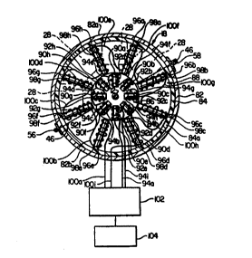
Referring to FIGS. 5 and 6, the sensing device 18 includes
a housing 82, a cylinder 84 disposed within the housing 82, and
first and second sensing arrays designated respectively by the
reference numerals 86 and 88. The housing 82 is divided into
upper and lower portions 82a and 82b which are connected by the
hinge 56 and the bracket 58, previously described. The
cylinder 84 includes a large diameter portion 84a and a reduced
diameter portion 84b for housing the second and ~irst sensing
arrays 88 and 86, respectively. Although not shown, it is
understood that the cylinder 84 may be divided into two
portions in a manner similar to the housing 82. It is
understood that the housing 82 is constructed of either a
magnetically conductive or nonconductive material and the
cylinder 84 is constructed of plastic or a similar magnetically
nonconductive material.
Eight sensing elements 90a-9Oh having helical wire
windings 92a-92h, respectively, comprise the first sensing
array 86. The elements 90a-9Oh are connected by fasteners (not
shown) to the inner wall of the reduced diameter portion 84b.
Windings 92a-92h are connected electrically in series by wires
94a-94i, as shown.
Eight sensing elements 96a-96h having helical wire
windings 98a-98h, respectively, comprise the second sensing
array 88. TXe elements 96a-96h are connected by fasteners (not
shown) to the inner wall of the large diameter portion 84a.
` ~ W093/19~ 2 1 ~ 2 7 1 7 PCT/US93/02~
Windings 98a-98h are connected electrically in series by wires
lOOa-lOOi, as shown.
The first and second sensing arrays 86 and 88 are
connected by the respective wires 94a, 94i and lOOa, lOOi to a
digital signal processor 102 and a microcontroller 104, as will
be discussed.
The elements 90a-9Oh and 96a-g6h are configured as rods
constructed of a ferromagnetic material and are positioned
perpendicular to the axis of and radially spaced around the
cable 12 undergoing testing. The ends of the elements 90a-9Oh
and 96a-96h are spaced apart from the cable 12 such that the
only direct contact of the magnetic interferometer 10 with the
cable 12 is by the roller guides 74. The elements 90a-9Oh are
positioned closer to the cable 12 than the elements 96a-96h,
for reasons subsequently discussed.
Th~ elements 90a-9Oh of the first sensing array 86 are
aligned in longitudinal planes which are the same for
corre~ponding pairs of the magnets 28, 80 that each of the
elements and corresponding magnet pairs share the same radial
center line from the cable 12, as depicted in FIG. 6. The
elements 96a-96h of the second sensing array 88 occupy
different longitudinal planeæ than the elements 90a-9Oh of the
first sensing array 86 for reasons subsequently discussed. The
elements 96a-96h are aligned in longitudinal planes which are
midway between the longitudinal planes of corresponding pairs
of the magnets 28, and the adjacent magnets 28, as shown in
FIG. 6, it being understood that alignment of the
elements 90a-9Oh and g6a-96h could be reversed.
The windings 92a-92h and 98a-98h are wound in order to
allow a voltage to be induced through the windings as a result
of the relative motion of the cable 12 as indicated by an arrow
106 producing perturbations in magnetic flux lines 108 and 110,
as will be discussed. The windings can either be continuously
wound or bifilar wound, with ~ifilar windings resulting in
increased amplitudes of the induced voltages.
Besides the speed and location sensor 80 and the first and
second sensing arrays 86 and 88, a Hall ef~ect sensor 112 is
also disposed within the magnetic interferometer lo to detect
WO93~1g380 PCT~US93/02~
2:~32717 lo-
the presence of magnetic flux for reasons discussed below.
Preferably and as shown on FIG. 5, the Hall effect sensor 112
is disposed within the first magnet housing 14 between one of
the magnets 28 and the inner end cap 32.
Referring to FIG. 7, a functional block diagram o~ the
digital signal processor 102 of the present invention is shown
which takes d~ta from the first sensing array 86, the second
sensing array 88, the speed and location sensor 80 and the Hall
e.ffect sensor 112, filters and processes the data as required,
and stores the data in memory for later retrieval and
subsequent processing by the microcontroller 104. The
processor 102 includes a power supply 114, a first sensing
array signal clarifier 116, a second sensing array signal
clarifier 118, a sensor signal modifier 120, an encoded
microprocessor 122, a microcontroller interface 124, a memory
manager 126 and a memory 128. The processor 102 is preferably
integral with the exterior of the magnetic interferometer 10 to
allow autonomous data collection. A RS 232 serial port 130 is
provided for connecting the processor 102 to the
microcontroller 104 to process the data. As the
microcontroller 104 is conventional, it will not be described
in any further detail.
In use~ the bolt 60 of the first magnet housing 14 is
removed and the corresponding bolts are removed from the
bracket assembly 54 of the second magnet housing 16 and the
bracket assembly 58 of the sensing device 18. The first magnet
housing 14, the second magnet housing 16, and the sensing
device 18, including their respective internal parts, are
opened by means of the respective hinges 48, 52 and 56, and the
magnetic interferometer 10 is positioned and closed to
concentrically surround a portion of the cable 12 to be tested.
As shown most clearly in FIGS. 1 and 2, the cable 12 is
engaged by the diametrically opposed roller guides 74 at
respective ends of the magnetic interferometer 10. By means of
the spring loaded shafts 68 which urge the roller guides 74 to
extend from and allow the roller guides 74 to contract within
the nousing 66, the magnetic interferometer 10 can accom~odate
a wide variety of cables having different diameters~ Also, by
'~
-`. W093/19 ~ 2 1 3 2 7 1 7 PCT/US93/02~
means of the roller guides 74, the cable 12 is centrally
located within the central bore 20 as previously discussed.
The magnets 28 disposed within the first magnet housing 14
and the second magnet housing 16 set up a magnetic flux
pattern, discussed below, that is detected by the sensing
device 18. When the magnetic interferometer 10 and the cable
12 are moved relative to each other in a conventional manner as
indicated by the arrow 106 in FIG. 5, any deviation in the
cross-sectional thickness of the cable 12 causes a perturbation
in the magnetic flux lines 108 and 110 set up by the plurality
of magnets 28 and this perturbation is detected by the sensing
device 18.
When the outer housings 22 of the first and second magnet
housings 14 and 16 are magnetic conductors, the magnetic
circuit is established across the outer housings 22 and is
co~pleted by the cable 12. When the outer housings 22 and the
housing 82 are made of ~ plas~ic material, they form no part of
the magnetic circuit and the magnetic circuit is established
between aligned sets of magnets 28 and is completed by the
cable 12. When the housings 22 and 82 are made of a
magnetically nonconductive mater~al, the magnetic circuit i8
mor~ highly concentrated ~n the cable 12, thereby increasing
the signal amplituda generated by a flaw in the cable 12, as is
discussed below.
As shown in FIG. 5, a leakage flux is established in the
air space around the cable 12 as represented by the magnetic
flux line 110. If the magnetic cross-section of the cable 12
is constant and the structural integrity of the cable 12 is
uniform, then the magnetic flux line 110 representing the
leakage flux and the magnetic flux within the aable 12,
represented by magnetic flux line 108, run parallel to the axis
of the cable 12. In the case of abrupt changes (hereinafter
"defe¢ts") in the magnetic cross-sectional area of the cable 12
cau~ed by, among other things, breaks, corrosive pits, loops or
corkscrews, the magnetic flux within and surrounding the cable
12 is perturbed and the magnetic flux lines 108 and 110 are
deflected. These perturbations or changes in the magnetic flux
result in a voltage being induced in both of the first and
WO g3/19380 PCr/USg3/02560 - '
213~717 12 -
second sensing arrays 86 and 88, the amplitude of which depends
upon the location and magnitude of the magnetic flux change.
The signal value of the induced voltage depends upon the size
and type of the defect and is proportional to the local change
of the magnetic croæs-sectional area of the cable 12.
The Hall effect sensor 112 is provided to detect gradual
changes in the magnetic cross-sectional area of the cable 12,
caused by, among other things, stretching, erosion and wear,
which cause deviations in the magnetic flux lines 108 and llo
within and surrounding the cable 12. These reductions or
gradual changes in the magnetic f}ux result in a change in the
voltage being induced in the Hall effect sensor 112. The
relative size of the voltage change induced in the Hall effect
sensor 112 is directly proportional to the local change of the
magnetic cross-sectional area of the cable 12 and can be used
for the automatic gain control of the signals produced by both
the first and second sen~ing arrays 86 and 88 and for
deter~ining the amount of wear and stretching of the cable 12.
It is underætood that each element 90a-9Oh and 96a-96h of
the first and second sensing arrays 86 and 88 will detect a
given defect in the cable 12, however a particular defect will
be morQ strongly detected by the particular element or elements
which are close~t in radial proximity to the location of the
defect. Since the elements 90a-9Oh occupy longitudinal planes
which are rotationally displaced relative to the elements
96a-96h, the signals produced by the first and second sensing
arrays 86 and 88, respectively, will be different according to
th~ radial location of the defect in the cable 12. The
placement of the elements 90a-9Oh of the first sensing array 86
closer to the cable 12 will increase the ability to detect
subsurface dQfects within the cable 12 and further
differentiate the signalæ produced by the first and æecond
sensing arrays 86 and 88, respectively. The respective
placement of the elements ~Oa-9Oh and 96a-96h thereby allows
the precise nature and location of a defect within the cable 12
to be determined due to the different effects each defect will
have on each element. Since the firæt and second æensing
arrays 86 and 88 are longitudinal displaced, it is understood
-~ W093/19~0 2 1 ~ 2 7 1 7 PCT/US93/02~
- 13 -
that one of the arrays will detect a defect prior to the otber,
depending on the direction of movement of the cable 12 relative
to the sensing device 18.
As shown in FIG. 7, the Hall effect sensor 112 tran~mits a
signal voltage proportional to the magnetic field strength of
the magnetic flux lines 108 and 110 to the sensor signal
modifier 120. The signal from the Hall effect sensor 112 is
used by the sensor signal modifier 120 to automatically adjust
the voltage level of the signals received from the first and
second sensing arrays 86 and 88, respectively. The first and
second sensing array clarifiers 116 and 118 filter the adjusted
first and second sensing array signals, respectively, and
attenuate any noise outside the center frequencies of the
clarifiers 116 and 118, preferably being 30 Hz and lOo Hz
respectively, to provide the sensor signal modifier 120 with
both filtered and unfiltesed signals. The sensor signal
modifier 120 then transforms the analog signals to digital
signals and provides the encoded microprocessor 122 with a
digital representation of the unfiltered first and second
sensing array signals, the filterQd first and second sensing
array signals and the Hall effect sensor signal.
The encoded microprocessor 122 also receives the already
digital data from the speed and location sensor 80. From this
additional data, the encoded microprocessor 122 determines the
present speed and location of the magnetic interferometer 10
and produces a data sample representing the signal from the
fir~t sensing array 8S, the signal from the second sensing
array ~8, the signal from the Hall effect sensor 122, the sum
of the signals from the first and second sensing arrays 86
and 88, the filtered signals from the first and second sensing
arrays 86 and 88, and the speed and location of the magnetic
interferometer 10. The memory manager 126 can then be used to
either store the data sample in the memory 128 or trans~it the
data sample to the microcontroller 104, depending on whether
the microcontroller 104 is connected to the processor 102.
In one mode of operation, the data samples are collected
at a rate of 8 bytes per sample and at 8 samples per inch of
cable and are stored in the on-board memory 128, thereby
W093/19~0 PCT/US93/02
2 1 3 2~ 1 7 ~ 14 -
providing the magnetic interferometer 10 with the capacity to
autonomously collect data. Subsequent to testing, the
microcontroller 104 i8 connected to the processor 102 via the
RS 232 ~erial port 130 so that the data samples can be
trans~erred to the microcontroller 104 which then interprets
the digital signals from the processor 102 in a manner to
quantify the condition of the cable 12 and to determine the
type and location of each defect in the cable 12. Alternately,
the microcontroller 104 can be connected to the processor 102
during testing, thereby providing the magnetic interferometer
10 with the ability to produce real time output and the
capacity to collect data samples from any length cable.
The encoded microprocessor 122 is encoded so as to prevent
operator access to the microcoded software internal to the
microprocessor 122. The microcontroller interface 124 is
therefore provided to allow the system operator to communicate
to the encoded microprocessor 122 and calibrate the magnetic
interferometer 10, as will be described.
As mentioned above, the microcontroller 104 interprets the
digital signals from the processor 102 in a manner to quantify
the condition of the c~ble 12 and to determine the type and
location of each def~ct in the cable 12. To this end, each of
the signals from the first and second sensing arrays 86 and 88,
the Hall effect sensor 112 and the speed and location sensor 80
may be transmitted to the microcontroller 104 individually and
in combination to perform integration and differentiation
operations between the signals. The individual, combined,
integrated and differentiated signals may then be interpreted
to obtain additi~nal information concerning the nature of the
defects in the cable 12.
FIG. 8 is a flow chart illustrating the initialization
program logic. It is understood that the logic is implemented
by computer instructions contained within the microcontroller
104. In block 132, the software operation begins with the
program initialization. In block 134, the software attempts to
interrogate the microprocessor 104 via communication line 1 and
c~ntrol is transferred to block 136. In block 136, the
software waits a predetermined period of time to determine if
~ ~ W093/19380 2 1 3 2 7 1 7 PCT/US93/02 ~
- 15 -
the microcontroller 104 is connected to the processor 102 via
communication line 1. If it is not so connected, control
proceeds to block 138 where the software attempts to
interrogate the microproce~sor 104 via communication line 2 and
control is transferred to block 140. In block 140, the
software waits a predetermined period of time to determine if
the microcontroller 104 is connected to the processor 102 via
communication line 2. If it is not 80 connected, control
proceeds to block 142 where the decision is made that the
microcontroller 104 is not connected to the processor 102 and
control is transferred to block 144. In block 144, the
microcontroller 104 displays the current status that the
microcontroller 104 is not connected to the processor 102, and
control is returned to the main menu in block 146.
If communication is established by either communication
line 1 or communication line 2 in blocks 136 or 140,
respectively, then control proceeds to block 148 where the
software establishes a communication link to provide the
current status. Control then proceeds to block 150 where the
microcontroller 104 receives the status of the processor 102.
Control then proceeds to block 144 where the microcontroller
104 displays th~ current st~tus of the processor 102 for a
predetermined time. The program displays a current status that
the processor 102 is idle, acquiring data, transferring data,
or that data is available for transfer, and control is returned
to the main menu in block 146.
FIG. 9 is a flow chart illustrating the control logic for
initialization of a header file. In block 152, the program
begins by displaying the main menu and the operator selects
option 1.0 to transfer control to block 154. In block 154, the
operator provides the program with header information, such as,
the operator's name, the test location, the time of the test
and other data as may be desired. In block 156, the input
header information is stored in a header file for subsequent
display and/or print out.
FIG. 10 is a flow chart illustrating the program logic for
the acquisition and transfer of data. In block 158, the
program begins with the operator selecting option 2.1.0 from
W093/19 ~ 2 1 3 2 7 1 7 PCT/US93/0~
- 16 -
the main menu which transfers control to block 160. In block
160, the program determines the current status of the magnetic
interferometer 10 which is idle, acquiring data, transferring
data or has data available for transfer, and then displays the
current status to the operator. Control is then transferred to
block 162 where the decision is made as to whether the magnetic
interferometer 10 is acquiring data. If the magnetic
interferometer 10 is acquiring data, then control is
transferred to block 164. In block 164, the operator has the
option of waiting until the magnetic interferometer 10 has
completed acquiring data. If the operator desires to wait,
then the program returns to block 160 until the status
changes. If the operator decides in block 164 not to wait for
completion of the data acquisition, then control is transferred
to block 170.
If the magnetic interferometer 10 is not acguiring data,
then control is transferred to block 166. In block 166, it is
determined if the magnetic interferometer 10 has data available
for transfer. If no data i8 available for transfer, then
control is transferred to block 168, and the program returns to
the main menu. If it is determined in block 166 that data is
available for transfer, then, as when the operator decides in
block 164 not to wait for completion of the data acquisition,
control i8 transferred to block 170. In block 170, the
operator is prompted as to whether data is to be transferred.
If the operator does not desire for data to be transferred,
then the control is transferred to block 168 and the program
returns to the main menu. If the operator does desire for data
to be transferred, then control is transferred to block 172.
In b}ock 172, a command instruction "S" is sent to the memory
manager 126 and the magnetic interferometer 10 responds by
echoing the command instruction back to the microcontroller
104. Control is then transferred to block 174.
In block 174, the microcontroller 104 reads the first data
sample which consists of, as previously mentioned, 8 bytes of
data, and control is transferred to block 176~ In block 176,
the microcontroller 104 determines if the end of the data file
~ has been reached. If the end of the data file has not been
; .
WOs3/193B0 PCT/US93/02~
2132717
- 17 -
reached, then control is transferred to block 178. In block
178, the microcontroller 104 stores the data sample in memory
and control is transferred back to block 174 to repeat the
procedure. If in block 176 it is determined that the end of
the data file has been reached, then control is transferred to
block 168 and the program returns to the main menu.
FIG. 11 is a flow chart illustratin~ the progra~ logic for
the calibration of the magnetic interferometer 10. In block
180, the program begins with the operator selecting option 2.2
from the main menu which transfers control to block 182. In
block 182, the operator has the option of selecting a numeric
value from 1 to 5 corresponding, respectively, to the voltage
output range for the first sensing array 86, the voltage output
range for the second sensing array 88, the analog to digital
converter sensitivity for the first sensing array 86, the
analog to digital converter sensitivity for the second sensing
array 88 and a cable stop counter.
In block 184, the microcontroller 104 transmits the
~elected numeric value to the éncoded microprocessor 122 via
the microcontroller interface 124 and control is transferred to
block 186. In block 186, the selected numeric value is echoed
back to the microcontroller 104 and control is transferred to
block 188. In block 188, the operator is prompted for the
first calibration data byte, the data byte is transmitted to
the encoded microprocessor 122, and control is transferred to
block 190. In block 190, the encoded microprocessor 122 echoes
the character ~lZ~l back to the microcontroller 104 and control
is transferred to block 192. In block 192, the operator is
prompted for the second data byte which is then transmitted to
the encoded microprocessor 122 and control is transferred to
block 194. In block 194, the encoded microprocessor 122 echoes
the character "Z" back to the microcontroller 104 and control
is transferred to block 196. In block 196, control is returned
to the main menu.
If in block 182 the operator of the microprocessor 104 had
selected a numeric value of 1 corresponding to the selection of
the voltage output range for the first sencing array 86, then
the first and second data bytes would correspond to the
WOg3/19~ - PCT/US93/02~
~1~2717
- 18 -
positive and negative voltage output levels for the desired
voltage output range for the first sensing array 86. I~ in
block 182 the operator had selected a numeric value of 2
corresponding to the selection of the voltage output range for
the second sensing array 88, then the first and second data
bytes would correspond to the positive and negative levels for
the desired voltage output range for the second sensing array
88. If in block 182 the operator had selected a numeric value
of 3 corresponding to the selection of the analog to digital
converter sen~itivity for the first sensing array 86, then the
first and second data bytes would correspond to the positive
and negative voltage sensitivity levels for the two respective
analog to digital converters for the first sensing array 86.
If in block 182 the operator had selected a numeric value of 4
corresponding to the selection of the analog to digital
converter sensitivity for the second sensing array 88, then the
first and second data bytes would correspond to the positive
and negative voltage sensitivity levels fox the two respective
analog to digital converters for the second sensing array 88.
If in block 182 the operator had selected a numeric val~e of 5
corresponding to the selection of the cable stop counter, then
the fir~t and se¢ond data bytes would correspond to the length
of the cable 12 to be measured and the period of time the
magnetic interferometer 10 is to be operating.
FIG. 12 is a flow chart illustrating the program logic for
the interrogation and reset of the internal clockJcalendar of
the magnetic interferometer 10. In block 198, the program
begins with the operator selecting option 2.2.6 from the main
menu and control is transferred to block 200. In block 200,
the microcontroller 104 interrogates the internal
clock/calendar, displays its current time and date, and then
control is transferred to block 202. In block 202, the
operator has the option to either reset the internal
clock/calendar or accept the currently displayed time and
date. If the operator decides that the currently displayed
time and date are acceptable, then control is transferred to
block 204 and the pro~ram returns to the main menu.
If the operator decides that the currently displayed time
~- w093/i9 ~ 2 1 3 2 7 1 7
-- 19 --
and date are not acceptable, then control is transferred to
block 206. In block 206, the correct time snd date are read
from the microcontroller 104 and control i8 transferred to
block 208. In block 208, a COD and signal is sent to the
magnetic interferometer 10 to accept the new time and date, and
control is transferred to block 210. In block 210, the program
waits for the command to be echoed back from the magnetic
interferometer 10, and when the command signal is returned,
contxol is transferred to block 212. In block 212, the desired
time and date are sent to the magnetic interferometer lo, and
control is transferred to block 214 where the program returns
to the m~in menu.
FIG. 13 is a flow chart illustrating the program logic to
print and display the acquired data samples having options
3.1.0, 3.2.0 and 3.3.0 in the main menu in block 216. If the
operator selects option 3.1.0 from the main menu, control is
transferred to block 218. _n block 218, the microcontroller
104 reads the header file and control is transferred to block
220. In ~lock 220, the microcontroller 104 reads the data
8ample8 and control is transferred to block 222. In block 222,
the microcontroller 104 evaluates the data samples, as
previously describQd, and formats the results for graphical
display and printout. Control is then transferred to block 224
in which the results are displayed and printed, and control is
transferred to block 226 where the program returns to the main
menu.
Tf in block 216, the operator selects option 3.2.0 from
the main menu, then control is transferred to block 228. In
block 228, the microcontroller 104 reads the header file and
control is transferred to block 230. In block 230, the
microcontroller 104 reads the data samples and control is
transferred to block 232. In block 232, the microcontroller
104 evaluates the data samples, as previously described, and
formats the results for numerical display, and control is
transferred to block 234. In block 234, the results are
displayed and printed, and control is transferred to block 226
where the program returns to the main menu.
I~ in block 216, the operator selects option 3 . 3 . 0 from
:
WOg3/19 ~ PCT/US93/02~
2132717
- 20 -
the main menu, then control is transferred to block 236. In
block 236, the microcontroller 104 reads the header file and
control is transferred to block 238. In block 238, the
microcontroller 104 reads the data samples and control i8
transferred to block 240. In block 240, the microcontroller
104 evaluates the data samples, as previously described, and
formats the numerical results for both graphical and numerical
display and printout, and control is transferred to block 242.
In block 242, the results are displayed and printed, and
control is transferred to block 226 where the program returns
to the main menu.
FIGS. 14-17 show another embodiment of the present
invention which also uses signals generated by perturbations in
a magnetic flux generated through a cable 244 to detect
structural anomalies in the cable 244. Referring specifically
to FIG. 14, a magnetic interferometer 246 is shown which is
adapted to concentrically ~urround the cable 244 to be tested
for structural anomalies. The magnetic interferometer 246
includes an outer housing 248 which is comprised of a plurality
of concentric, cylindrical plastic pipes 250a-250f which
collectively enclose a first magnet housing 2S2, a second
magnet housing 254, both of which have end caps 256 located at
each of their respective ends, and a sensing device 258
dispoaed between the fir~t magnet housing 252 and the second
magnet housing 254. The cable 244 is centrally located within
a central bore 260 (see FIGS. 15-17) which runs the entire
length of the magnetic interferometer 246 from the first magnet
housing 252, through the sensing device 258, and through the
second magnet housing 254.
In this embodiment of the present invention, the outermost
pipe 250a extends over and between the two outermost end caps
256 of the interferometer 246. The pipes 250b and 250c, like
the pipe 250a, also extend between the two outermost end caps
256, but they abut the interior walls of the outermost end caps
256, respectively. The pipe 250d only encloses the first
magnet housing 252, the pipe 250e only encloses the second
magnet housing 254, and the pipe 250f only encloses the sensing
device 258, as will be described.
W093/19~ 3 ~ 7 1 7 PCT/US93/02
- 21 -
Concentrically disposed within each of the pipes 250d and
250e, respectively, is an inner housing 262 of nonmagnetically
conducting material which, preferably, i8 a cylindrical plastic
sleeve. A plurality of permanent magnets 264 are disposed
between the pipes 250d and 250e and the inner housings 262,
respectively, and are arranged to form segmented cylinders
spaced apart from and surrounding the cable 244 with all of the
magnets 264 being disposed such that the same pole of each of
the m~gnets 264 is facing inward toward the cable 244, it being
understood that the magnets 264 within the second magnet
housing 254 have the opposite pole facing inward toward the
cable 244 than the pole facing inward within the first magnet
housing 252.
Once the magnets 264 are positioned, the voids between the
magnets 264 are filled with a nonmagnetically conducting
material 266 to maintain the magnets 264 within the first and
cecond magnet housings 252 and 254, respectively.
It ~hould be understood that although the pipes 250a-250e,
the inner housing 262 and the material 266 have all been
described as cepar~te elements, they could all be formed as a
single element, such as by plastic in~ection molding
Referring to FIGS. 14 and 16, attached to the exterior end
cap 256 of the first magnet housing 252 is a pair of
di~metrically opposed roller guide assemblies 268. A
complementary pair of diametrically opposed roller guide
assemblies 268 is also attached to the exterior end cap 256 of
the second magnet housing ~54. Each roller guide assembly 268
includes a houæing 270 and a roller bracket 272. Each roller
bracket 272 retains an axle 274 with a roller guide 276 mounted
on each axle 274.
Referring to FIG. 14, it is seen that one af the roller
brackets 272 of each roller guide assembly 268 is securely
attached to its housing 270 whereas the roller bracket 272 on
the diametrically opposed roller guide assembly 268 is slidable
- within a guide 278. A pin 280 extends outwardly from each
roller bracket 272 and extending between opposing pairs of
which are springs 282 to urge the roller brackets toward each
other so that the roller guides 276 securely engage the cable
.
WO 93/lg380 PCr/USg3/02560
2132717
- 22 -
244. The springs 282 allow the magnetic interferometer 246 to
be able to aeeommodate a wide variety of eables having
different diameters.
The magnetie interferometer 246 preferably ineludes a
speed and loeation sen~or 284 (FIG. 14) identieal to the speed
and loeation sensor 80 of the previously deseribed embodiment,
and thus it will not be rede~eribed here in detail.
Referring to FIGS. 16 and 17, the sensing deviee 258
ineludes a housing 286, first and seeond sensor retainers 288
and 290 eoneentrieally disposed within the housing 286, and
first and seeond sensing arrays 292 and 294 retained by the
first and seeond sensor retainers 288 and 290, respeetively.
The first sensor retainer 288 is disposed within the seeond
sensor retainer 290, and the seeond sensor retainer 290 is
sized to press fit within the housing 286. The housing 286,
sized to press fit within the pipe 250f, is eonstrueted of
either a magnetieally eonduetive or noneonduetive material
while the first and seeond sensor retainers 288 and 290 are
eonstrueted of ferrous metal or a similar magnetieally
conductive material, it being understood that the first and
seeond sensor retainers 288 and 290 are magnetieally insulated
from one another as is deseribed below.
The first sensor retainer 288 is eomprised of a rolled
channel iron 288a having an inwardly faeing ehannel and a
eomplementary ring 288b positioned at the perimeter of the
ehannel. The ehannel iron 288a includes eight symmetrieally
spaeed tapered bores 296a-296h, and the ring 288b ineludes
eight eorresponding threaded bores 298a-298h whieh when aligned
with the bores 296a-296h are adapted to threadingly receive
eight sensing elements 300a-300h. The channel iron 288a also
ineludes two diametrically opposed tapered bores 302a and 302b,
the purpose of which is described below.
Similarly, the seeond sensor retainer 290 is comprised of
a rolled ehannel iron 290a having an inwardly faeing ehannel
and a eomplementary ring 290b positioned at the perimeter of
the ehannel. The ehannel iron 290a includes eight
symmetrieally spaeed tapered bores 304a-304h, and the ring 290b
ineludes eight corresponding threaded bores 306a-306h which
, :~
wos3/19~o 2 1 3 ~ 7 1 7 PCTlUSg3/02~
- 23 -
when aligned with the bores 304a-304h are adapted to
threadingly receive eight sensing elements 308a-308h.
Two of the elements 308a-308h which are diametrically
opposed, namely elements 308a and 308e as shown in FIG. 17,
have internally threaded bores 310a and 310b, respectively,
which when aligned with the bores 302a and 302b are adapted to
receive bolts 312a and 312b which rigidly secure the first and
second sensor retainers 288 and 290 together. The bQlts 312a
and 312b are preferably a nonmagnetically conducting material
to prevent magnetic flux from flowing between the first and
second sensor retainers 288 and 290.
The elements 300a-300h and 308a-308h are configured as
rods constructed of a ferromagnetic material and are positioned
perpendicular to the axis of and radially spaced around the
cable 244 undergoing testing. The ends of the elements
300a-300h and 308a-308h are spaced apart from the cable 244
such that the only direct contact of the magnetic
interferometer 246 with the cable 244 is by the roller guides
276.
As shown in FIG. 16, the elements 300a-300h of the first
sen~ng array 292 are aligned in longitudinAl planes which are
the same for corresponding pairs of the magnets 264 such that
they are aligned with the inner half of the magnets 264. The
elements 308a-308h of the second sensing array 294 occupy
different longitudinal planes than the elements 300a-300h of
the first sensing array 292 and are aligned in longitudinal
planes which are midway between the longitudinal planes of
corresponding pairs of the magnets 264, and the ad;acent
magnets 264. The elements 308a-308h are positioned within the
second sensor retainer 290 such that they are aligned in line
with the outer half of the magnets 264.
The elements 300a-300h each have helical wire windings
314a-314h, respectively, which comprise the first sensing array
292. Windings 314a-314h are connected electrically in series
and can either be continùously wound or bifilar wound, with
bifilar windings resulting in increased amplitudes of the
induced voltages.
The elements 308a-308h each have helical wire windings
. ~ ~
,
W093tlg~ PCT/US93/02~
21~717 24 -
316a-316h, respectively, which comprise the second sensing
array 294. Windings 316a-316h are connected electrically in
series and can either be continuously wound or bifilar wound,
with bifilar windings resulting in increased amplitudes of the
induced voltages.
The first and second sensing arrays 292 and 294 are
connected by wires 318, 320 and 322, 324, respectfully, to a
digital signal proce~sor 326 and a microcontroller 328, which
are identical to the digital signal processor 102 and the
microcontroller 104 of the previous embodiment and thus will
not be redescribed here in detail.
A Hall effect sensor 330 is also disposed within the
magnetic interferometer 246 of the present embodiment as shown
in FIG. 16 which functions identically as the Hall effect
sensor 112 of the previous embodiment.
In a manner similar to the previously described
embodiment, all of the parts of the magnetic interferometer 246
are split in half by means of a medial slit 332, the split
ha}ves of which are maintained in facing relationship by a
hinge ~nd bracket a~embly 334, thereby allowing the magnetic
interferometer 246 to be opened and placed around the cable 244
and operated in a manner consistent with the previously
de~cribed operation of the invention.
While the pre~ent invention has been described in detail
and with reference to specific examples thereof, it will be
apparent to one skilled in the art that various changes and
modifications can be made therein without departing from the
spirit and scope thereof.
For example, the sensing arrays need not be wired in
series as previously described. If more information regarding
the nature and location of a defect is required, the individual
sensing elements can each be diroctly wired to the processor.
Further, the speed and location of the magnetic interferometer
can be determined by the sensing arrays, thereby eliminating
the need for the speed and location sensor in one of the roller
guides. Specifically, the sensing arrays can be used to detect
the lay lines of the cable being tested since they produce
deviations in the magnetic flux. Once the number of lay lines
wo93/1s~ PCT/US93/02~
213~717
- 25 -
per unit length of cable is determined, the speed and location
of the magnetic interferometer can be determined by counting
the lay lines passed over. In addition, the ~ensing arrays can
be comprised of Hall effect sensors rather than as described.
Also, whereas the processor 102 has been described as having a
memory 128 separate from its other components, it is understood
that the encoded microprocessor 122 has memory which could
function as the memory 128.
~ t ~hould also be noted that although the magnetic
interferometer of the present invention has been described in
relation to use with metal wire rope or the like, the invention
disclosed can be used to find flaws and defects in any material
in which such flaws or defects cause perturbations of a
magnetic flux passing through the material.
A latitude of modification, change and substitution is
intended in the foregoing disclosure and in some instances some
features of the invention will be employed without a
corresponding use of other features. Accordingly, it is
appropriate that the appended claims be construed broadly and
in a manner consistent with the scope of the invention.
,~ .