Note: Descriptions are shown in the official language in which they were submitted.
CLE-1
SYSTEM FOR MONITORING THE INSULATION QUALITY OF STEP
GRADED INSULATED HIGH VOLTAGE APPARATUS
DESCRIPTION
Technical Fipl~
Applicant's invention relates generally to a system which
monitors and measures the insulation status with respect to
earth ground of a high voltage electrical network and more
particularly to a system that quantitatively measures the
capacitively coupled charging current in a step-graded paper and
foil insulation system to produce a signal output proportional to
the current for continuous monitoring and alarm level detection
to indicate the possibility of failure for the entire insulating
system.
ackground Art
Step-graded foil and paper insulation systems are generally
employed on high voltage measurement and control apparatus
such as current transformers for the purposes of protecting
personnel from shock hazard and electrical instrumentation from
equipment damage. Multiple alternating layers of foil and paper,
with the foil layer of least potential being earth grounded, are
used to form an effective series capacitive divider circuit
between the high voltage conductors and ground potential. Oil
impregnation of the paper dielectric is generally used in oil-
filled instrument transformers, power transformers, condenser
bushings and other apparatus for high voltage electrical power
systems.
Most step graded insulation systems are designed such that
the capacitance of each foil layer is equal, thus producing an
equal voltage stress on the dielectric betwaen each foil layer
when the apparatus is energized at high voltage. In designs
where each layer is of equal capacitance, the total capacitance
of the insulation system is equal to the layer capacitance divided
by the total number of layers. A charging current through the
capacitive circuit exists and is directly proportional to the
product of the lime voltage, the line frequency, and the total
_ CLE-1
2
capacitance. With the line voltage and frequency relatively
constant, changes in the insulation charging current are due
primarily to a degradation in the insulation system. Electrical
breakdown between layers results in degradation of the oil purity
which leaves carbon deposits, providing a conductive path which
effectively constitutes a short circuit between adjacent foil
layers. The total capacitance of an insulator exhibiting such
degradation increases as the effective number of foil layers is
reduced. This increase in total capacitance will increase the
charging current. Furthermore, each of the remaining layers is
subjected to an increase in voltage stress. Ultimately, as
additional foil layers break down, the residual voltage stress
between the remaining layers may exceed safe operating levels,
leading to the eventual, often catastrophic, failure of the entire
insulation system.
Conventional high voltage measurement and control
equipment which employ foil and paper step-graded insulation
offer no inherent means for monitoring the insulation charging
current. Methods have been developed for monitoring the
condition of the insulation apparatus. Most of them employ off-
line methods. A power factor test requires that the system be
energized with a test voltage and changes in the measured power
factor or capacitance over time are recorded to see if there are
any significant changes that would indicate a shorted layer.
Partial discharge methods are effective in detecting these
changes, but must be performed off-line and may not be practical
in installations where interruption of service is not economical.
Another method, gas-in-oil analysis, requires an oil sample to be
drawn and tested to determine the presence of various gas that
are generated when the apparatus overheats, usually indicative
of a breakdown of the insulation. Some other prior art systems
employ a measuring resistor in series with the ground loop and
measure the voltage generated by the leakage current. However,
direct measurement of this voltage is often misleading due to
lack of compensating networks due to the influence of the
capacitance of the insulation and effects of electrical
CA 02133047 2002-05-07
3
interference. Sensing the insulation charging current may not be
satisfactorily
accomplished by means of a resistive series element in the grounded electrode
or by
means of a ferrous magnetic core device. In either the resistive or ferro-
magnetic
sensing method, the capacitive nature of the insulation circuit between the
high
voltage conductor and ground is disturbed by a resistive or inductive sensor
to the
point where the magnitude of the insulation current is altered. U.S. Patent
No.
4,896,115 describes an on-line improvement over these common methods for
monitoring the quality of electrical network insulation by coupling a
reference AC
signal into the system and using electronic detection circuits to determine
the
leakage or ground fault impedance. Other methods inject a current at a lower
frequency than the network and detecting the resultant current flow in the
effective
leakage resistance and capacitance.
These methods, being applied off-line, are incapable of continuously
monitoring for a change in the insulation charging current while the apparatus
is in
operation. Further, they are often intrusive to the hermetically sealed
insulation
common to these types of insulation systems.
Summary of the Invention
Accordingly, it is desirable to provide a method and apparatus for the
continuous, on-line, conversion of the charging or leakage current of a step-
graded
insulated high voltage apparatus to a signal proportional to the leakage
current.
It is also desirable to provide an apparatus for comparing the signal
proportional to the charging current with predetermined levels to indicate a
change in
the integrity of the insulation of the high voltage apparatus.
It is also desirable to provide a method and apparatus for providing a remote
location for the conversion apparatus with respect to the comparison
apparatus, and
to provide a method and apparatus for monitoring the leakage current of single
phase and the leakage currents of polyphase high voltage systems.
CA 02133047 2002-05-07
4
According to one aspect of the invention there is provided an insulation
monitoring system for measuring a charging current through an insulation
system
between a high voltage conductor and earth ground, said insulation monitoring
system comprising an AC current sensor for converting said charging current to
a
first signal; a transmission network; a transmitter coupled between said AC
current
sensor and said transmission network, said transmitter having electronic
circuit
means for converting said first signal to a DC current and modulating a second
signal by said DC current for transmission over said transmission network,
said
second signal proportional to said charging current; a controller coupled to
said
transmitter by said transmission network to receive said second signal, said
controller for demodulating said second signal to extract said DC current,
converting
said DC current to a voltage proportionally to said charging current,
comparing said
voltage with a preset voltage level, and generating an alarm signal when said
voltage
exceeds said preset voltage level; and wherein said insulation monitoring
system
continuously monitors said insulation system.
According to another aspect of the invention there is provided a method of
monitoring insulation between a high voltage conductor and earth ground, said
high
voltage conductor and said earth ground comprising part of a high voltage
system,
said insulation monitoring method comprising converting a charging current
between
said high voltage conductor and said earth ground to a first signal
proportional to
said charging current; rectifying said first signal to a DC voltage;
modulating a
current loop with said DC voltage to produce a DC current signal proportional
to said
charging current for transmission to a remote location; demodulating said
current
loop at said remote location to extract said DC current signal; converting
said DC
extracted current signal to a second signal proportionally to said charging
current;
comparing said second signal with a plurality of preset voltage levels, each
of said
plurality of preset levels representative of varying multiples of said
charging current
and having a predetermined alarm time delay period; and generating an alarm
signal
for each of said plurality of preset voltage levels when said second signal
exceeds
said preset voltage level and said predetermined alarm time delay.
CA 02133047 2002-05-07
In the preferred embodiment of the invention, the invention is comprised of a
system of essential elements including, but not limited to, a remote sensing
coil
5 producing a voltage output linearly proportional to the insulation charging
current, a
remote, self powered electronic circuit coupled to the sensor which modulates
a DC
current control circuit proportionally to the output voltage of the sensor,
and an
electronic control circuit providing a suitable voltage supply for the
modulated current
and alarm threshold detection circuits.
The sensing coil described by the present invention utilizes a low
permeability core, which may be in the form of a toroid, wound with a high
number of
turns to create a low inductance linear coupler from which an output voltage
signal is
produced which is proportional to the current in the grounded conductor
passing
through the center of the toroid. The linear coupler also serves to
electrically isolate
the sensor electronic circuits from the insulation grounding system.
The monitoring system uses a signal current modulation scheme which
includes a 4 milliampere (mA) zero offset from which electrical power is
derived for
the remote electronic circuits and which serves to indicate that the
electronics are
functioning properly, even in the absence of insulation current. The zero to
full scale
modulation of 4 to 20 mA is used to conform to existing standards for
auxiliary
monitoring instruments, indicating meters, annunciators and alarm devices
which
may be series connected to the control current loop for additional supervisory
and
reporting capability. The midpoint between 4 mA and 20 mA is selected to
represent
the insulation current at its expected level for normal power system voltage
and total
insulation capacitance. That is, when the power system is energized at its
nominal
operating voltage and the total insulation capacitance has not been degraded
from
its intended initial value, the insulation charging current, will be equal to
a
nominal value for which the electronic circuits will cause an additional 8 mA
to flow in
the control current loop thereby causing a total of 12 mA in the loop. The
electronic
circuit is adjusted such that this same insulation charging current will
produce a full
scale control loop current reading of 20 mA when the insulation current
reaches a
CA 02133047 2002-05-07
(a)
value equal to twice its nominal value. Due to the proportionality of the
power system
voltage and the insulation capacitance to the insulation charging current, a
doubling
5 of the insulation charging current at nominal power system voltage would
indicate
that the total insulation capacitance has achieved a level of twice its
nominal value,
indicating that one half of the foil and paper layers in the insulation system
have
become ineffective. Alarm system thresholds may then be set between the 12 mA
and 20 mA control loop current levels to indicate the degree of insulation
breakdown
that can be tolerated before further measures are taken to investigate the
condition
of the insulation system.
The system controller includes a DC voltage source from which the remote
sensor electronics power supply and the modulated control loop current are
derived.
The controller may also include alarm circuits whereby alarm thresholds may be
established and alarm contacts made to transfer when the control loop current
exceeds predetermined adjustable limits. Since the insulation charging current
is
directly proportional to the power system voltage, and switching transients
may
regularly occur on the power system, these transient voltage levels on the
power
system will momentarily cause the insulation charging current, and hence the
control
loop current, to increase above their steady state levels. The alarm threshold
circuits
within the controller provide a predetermined delay period before initiating
the
transfer of the alarm contacts. This distinguishes between a short term
occurrence of
a switching voltage transient and a long term steady degradation of the
insulation
system as evidenced by a steady increase in the insulation charging current. ~
CLE-1
6
Other features and advantages of the invention, which are
believed to be novel and nonobvious, will be apparent from the
following specification taken in conjunction with the
accompanying drawings in which there is shown a preferred
embodiment of the invention. Reference is made to the claims
for interpreting the full scope of the invention which is not
necessarily represented by such embodiment.
Brief Descrio, tion_ of the Drawinas
FIG. 1 illustrates the construction of a step graded foil and
paper insulator showing the alternating layers of foil and paper.
FIG. 2 is an electrical schematic of the capacitive divider
circuit formed by the insulation structure of Fig. 1.
FIG. 3 is a block diagram of the essential elements in the
monitoring system of the present invention.
F1G. 4 is. a typical installation of the monitoring system of
Fig. 3 on an instrument transformer.
FIG. 4a is a schematic diagram of a portion of Fig. 4.
FIGS. 5a and Sb are a detailed block diagram of the monitoring syst~n
of the present invention as shown in Fig. 3.
FIG. 6 is a detailed schematic diagram of the remote sensor
illustrated in Fig. 5.
FIGs. 7a, 7b, 7c and 7d are detailed schematic diagrams of the
controller illustrated in Fig. 5.
Although this invention is susceptible to embodiments of
many different forms, a preferred embodiment will be described
and illustrated in detail herein. The present disclosure
exemplifies the principles of the invention and is not to be
considered a limit to the broader aspects of the invention to the
particular embodiment as described.
FIG. 1 shows the typical construction of a step-graded
paper and foil insulation system 1 where the high voltage
conductor 2 is wrapped with alternating layers of paper 4 and
conductive foil 6. Thus, as the foil layers are added to the
insulation system, the radius from the high voltage conductor to
CLE-1
7 ~1~~~-?'~
the foil layers tends to increase. The capacitance value between
any two adjacent foil layers is directly proportional to the
length of the layer and inversely proportional to the LOG ratio of
the outside to inside radius of the layer. in order to maintain
equal capacitance values from layer to layer, the length of the
foil layers are adjusted to account for the radial buildup. This
construction serves to insulate the outermost layer 8, usually at
ground potential, from the high voltage conductor 2.
A simplified electrical schematic diagram of the insulation
system 1 as it forms a series capacitance circuit from the high
voltage conductor 2 to ground 10 is shown in FIG. 2. With the
number of capacitors equal to the total number of foil layers, a
capacitive voltage divider 12 is formed. The total capacitance of
the series capacitors, with equal valued capacitors, is equal to
the layer capacitance divided by the number of layers. The actual
equivalent circuit will consist of many parallel capacitors
created by the capacitances that exists between noncandidate
layers. The electrical current 14, also called the charging
current, which flows through the capacitor circuit is
proportional to the voltage of the high voltage conductor 2 and
the total capacitance 12, based on the relationship that
s V ' ~w ' Ctotal
where Ctotal ~ 1 /C1 + 1 !C2 + 1 /C3 + 1 /C4
On a typical 345kV high voltage current transformer, the
total capacitance may be approximately 705 pf. Operating on a
345kV line, the line to ground voltage is about 200 kV and the
charging current 14 is nominally 53 mA. Under normal operating
conditions, the high voltage AC signal 2 has a relatively constant
amplitude and frequency. Thus, the charging current 14 remains
relatively constant in amplitude and frequency as well. Changes
in the capacitive insulation structure, however, will produce
changes in the amplitude of the charging current. Using the
circuit shown in Fig. 2 as an example, a voltage breakdown
CLE-1
~~ X30 ~'~
between two adjacent foil layers will effectively reduce the
total number of layers by 1, which in turn increases the total
capacitance 12 by a factor of 1/3. This will cause a
proportionate increase in the charging current 14 to over 30 mA.
Although Fig. 2 only shows four layers, more typical systems
will use 10 to 30 layers, depending on the voltage class of the
unit.
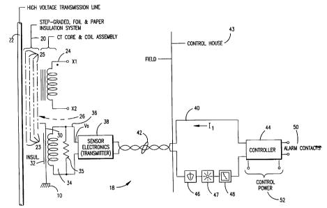
FIG. 3 illustrates an entire insulation current monitoring
system 18 in a block diagram according to the present invention.
A step-graded foil and paper insulation system 20 insulates a
high voltage conductor 22 from a transformer core and coil
assembly 24. The lowest potential foil layer 26 is electrically
connected to ground 10 with a conductive element 30 which
provides a ground path for the insulation charging current 32. A
wound, non-ferrous toroidal coil assembly 34 is positioned such
that the ground conductor 30 passes directly through the center
of the toroidal coil, such that the coil 34 links all of the
magnetic flux generated by the charging current 32 passing
through the conductor 30. The non-ferrous nature of the coil
assembly 34 results in a low inductance coupling back into the
series capacitive circuit of the insulation 20 and, therefore, does
not alter the magnitude of the charging current 32 being
measured. A burden resistor 35 internal to the assembly 34
produces a voltage Vs that is proportional to the charging current
32. The coil assembly 34 also serves to electrically isolate the
current monitoring system circuits 18 from the insulation
grounding system. Because of the high voltage and currents
associated with the system, the coil assembly will have some
type of shielding to prevent inductive coupling of adjacent and
unwanted magnetic fields.
The coil assembly 34 is electrically connected to a sensor
electronic circuit or transmitter 38 by means of a shielded,
twisted pair, or other suitable, cable 36. The transmitter 38
performs the functions of amplifying and rectifying the sensor
voltage signal Vs. Output driver circuits in the transmitter 38
are used to modulate a DC current 11 in a control loop 40. The
CLE-1
modulation results in the current signal 11 containing a
proportionate magnitude of the charging current 32. The control
loop 40 conforms to a standard 4-20 mA loop and the cable 42
which electrically connects the transmitter 38 to a controller 44
is also a shielded, twisted pair or other suitable cable. The
controller 44 may be located in a benign control house 43
environment. The control house 43 and the transmitter 38 can be
separated by up to 1,000 feet. Auxiliary devices may include
meters 46, alarms 47 or recorders 48 that can accept the 4-20
mA signal and are series connected in the control loop 40 to
provide additional control or monitoring functions.
Controller 44 performs one or more essential functions.
The controller 44 includes a DC voltage source, which may
provide as much as 30 to 40 volts, and which has the capability
of providing 20 mA full scale modulated current in the control
loop 40. The current which flows from the voltage source is
strictly modulated by the sensor electronics alone, yet the
terminal voltage across the controller 44 output is determined
by a nominal voltage level required to excite the remote power
supply circuits in the transmitter 38, and by the voltage drops
associated with the current in the control loop 40 and the
impedance of any auxiliary devices 46-48. The output of the
controller 44 are alarm contacts 50 which operate at a
predetermined, settable level of leakage or charging currant 32
to indicate a change in the insulation charging current 32 of the
insulation system 20. If a polyphase system is being monitored,
the controller 44 is capable of receiving inputs from
transmitters and control loops similar to transmitter 38 and
control loop 40.
The insulation current monitoring system 18 is powered by
control power 52 which is inputted to the controller 44. The
signal current modulation scheme includes a 4 mA offset zero
from which electrical power is derived for the remote
transmitter 38, eliminating the need for auxiliary power at the
high voltage apparatus that is being monitored.
CLE-1 .
FIGS. 4 ark 4a shag a typical installation of the insulation current
monitoring system. An instrument transformer 51, utilizing a
step graded foil and paper insulation system, is shown with the
tank 52 at ground potential and the grounded lead 30 from the
5 insulation system brought through the tank wall 52 and the
sensing coil 34 before being electrically grounded to the tank 51
itself. The insulation charging current 32 which flows through
conductor 30 is sensed by the sensing coil 34, whose output
signal Vs is then coupled by cable 36 to the transmitter 38 so as
10 to modulate the current 11 in the control loop 40 coupled by cable
42 to the controller 44 in the control house 43. The controller
44 provides remote power to the sensor electronics and monitors
the charging current levels in the control current loop 40 as
previously described. Only a single phase system is shown and
would be typical of a retrofit. As an alternative, the sensing coif
could be located inside the tank 52 immersed in oil, for instance.
Operation of the insulation current monitoring system 18
can be best understood with reference to FIGS. 5a and 5b together are a
detailed block diagram of the preferred embodiment of the
present invention. The grounded foil layer 26 has its ground lead
pass through the sensing coil 34 'such that the output voltage
Vs of sensor 34 is proportional to the insulation charging current
32 and is coupled to the transmitter 38, For the low leakage
currents being measured, it has been found that a proportionality
25 factor or ratio of fifty microvolts per one miliampere of
charging current provides an adequate degree of sensitivity. A
combination filter, amplifier and rectifier circuit 54 develops a
DC voltage signal 56 from voltage Vs that remains proportional
to the charging current 32. A voltage controlled current source
30 58, where the generated current is proportional to the voltage
56, is used to modulats a 4-20 mA current loop 40 for inputting
to channel A of controller 44. Controller 44 is shown for a three
phase system, but with only phase A sensor 34 and transmitter
38 shown. Additional sensors and transmitters would be
required for a three phase system.
CLE-1
11
The current 11 flowing in the current loop 40 is coupled to
the controller via a twisted pair cable 42 as previously detailed.
The current controlled current source 62 is calibrated such that,
for zero charging current 32, i.e., the high voltage apparatus
being monitored is not energized, 4 mA of quiescent current is
flowing in loop 40. This quiescent current is used to provide
power for the sensor 34 and transmitter 38. With the high
voltage apparatus energized during initialization, usually during
installation, the voltage controlled current source 58 is adjusted
to provide 12 mA of loop current. This represents the expected
charging current 32 when the high voltage apparatus is operating
at its nominal operating voltage. Thus 100 % (1 X) of initial
charging current equals 8 mA. Since there is a linear
relationship between the charging current 32 and the loop
1 5 current 11, 200% (2X) of charging current will equal 2 x 8 mA or
16 mA which is added to the 4 mA of quiescent current to create
mA of loop current 11. A current mirror 64 generates a
voltage V1 across resistor 66. V1 is calibrated to be
proportional to the charging current 32.
20 A 2X threshold level generator 68 and an adjustable 1.2-2X
threshold level generator 70 generate voltage levels V2, V3,
respectively. V2 is set such that voltage Vi, with 20 rnA of loop
current 11, will equal V2. V3 is adjusted within the range 1.2-2X
or 13.6-20 mA of loop current 11 for a similar relationship with
V1. Schmitt trigger 72 compares V1 with V2 and will enable
delay counter 1 when V1 exceeds V2, indicative of an increase in
the charging current 32 to a level that is twice the original
current resulting from a breakdown in the insulating layers of
high voltage apparatus. Schmitt trigger 74 compares V1 with V3
in a similar fashion.
Since switching transients may regularly occur on the
power system, voltage levels on the power system will
momentarily cause the insulation charging current 32, and hence
voltage V1, to increase above their steady state levels when such
transient conditions occur. Delay counters 1-6 provide a
predetermined delay period before initiating the transfer of the
CLE-1
~~.~'~0 ~r~
12
alarm contacts 50a, b. This distinguishes between a short term
occurrence of a switching voltage transient and a long term
steady degradation of the insulation system as evidenced by a
steady increase in the insulation charging current. Clock 75
produces a timing pulse 76 for the delay counters 1, 3 and 5,
with a divide by ten circuit 77 providing timing pulse 78 having a
longer time delay for counters 2, 4, and 6 that monitor the lower
levels of charging current 32 in the 1.2-2X range. The clock rate
for the 2X alarm level is adjustable and can provide up to 30
seconds of delay.
If the charging current 32 exceeds the 2x or adjustable
thresholds 68, 70 for a period longer than the time duration of
the delay counters 1-6, outputs 79 or 80, depending on which
threshold was exceeded, will energize latching switches 81, 82
respectively. This will in turn energize the 2X or 1.2-2X alarm
contacts 50a or 50b respectively through one of the "0R° function
84, 86. Alarm indicators 88a or 88b will display the appropriate
cause of the trip. The outputs will remain in a tripped state
until a master reset 90 is operated. Latching switches 81, 82
are used so as to provide memory of the condition if control
power is interrupted at any time after a trip operation.
Channels B and C will perform in the same manner. OR 84
will operate the 2X alarm if any of the three phases exceeds the
2X level far the preset time delay period and OR 86 will operate
the 1.2-2X alarm if any of the three phases exceeds that level for
the other preset time delay period. Power for the system is
supplied by a switchmode regulator 92, the details of which are
well known and are not an object of the present invention.
FIG. 6 details the transmitter 38 consisting of the rectifier
circuit 54 and voltage controlled current source 58. Current loop
is connected to terminals TB1-1 and TB1-2. The 4 mA
quiescent current of the loop current 11 creates a 6 volt rail
between 102 and 104 through the action of zener diode VR1 and
transistors Q2a, b, and c. The 4 mA of current flowing in the
35 current loop 40 is sufficient to provide base drive at node 110
for darlington connected transistors 02b and c. Transistor Q2a
CLE-1
13
will conduct, allowing zener diode VR1 to also conduct, building
a voltage at node 110. Regardless of any increase in the loop
current, the rail voltage will remain relatively constant and
regulated near the 6 volt level.
The output voltage Vs of sensor 34 which is proportional to
the insulation charging current 32, is inputted to terminals
TB1-3 and TB1-4. Changing the resistance values of resistors RA
and RB provide a means for using the insulation current monitor
18 for different levels of charging current 32, based on the
magnitude of the high voltage line and the total capacitance of
the insulated apparatus that the insulation current monitor 18 is
monitoring. These resistors, along with potentiometer RV1,
scale the incoming voltage Vs to the fixed gain of buffer
amplifier 106, which can be an operational amplifier for greater
temperature stability. The gain is selected such that AC output
voltage V4 does not saturate at the 200% level of allowable
insulation charging current 32. Since Vs is scaled to be fifty
microvolts per one milliampere of charging current, the gain of
the amplifier 106 has to be quite high. A two stage cascaded
amplifier is employed with the first stage, amplifier 106
providing half of the required gain so as to allow the full peak to
peak voltage swing of Vs to be amplified within the voltage rails
102, 104. The higher gain of the first stage will also reduce the
effects of the DC offset levels of the operational amplifiers on
the following stages, amplifiers 107 and 108 which only will
require a gain of -3 and +3, respectively, and the full wave
rectification circuitry. Capacitor C2 couples voltage V4 to
amplifiers 108 and 110 which function to generate voltages V5,
V6 respectively, that are equal, but phase shifted by 180 degrees.
As a result, resistor R16 becomes a load resistor that produces a
full wave rectified voltage V7, which is the DC voltage signal 56
as referenced in Fig. 5, through the alternate conduction of
transistor pairs Q1 a, Q1 c and Q1 b, Q1 d. Voltage V7 is positive
with respect to the voltage rail 104. RC network C4-R17
provides a DC filter for the rectified voltage V7 and the C3-R15
combination provides a balance with the positive DC rail 102.
l:~.C-1
14
Calibration of the rectifier circuit 54 is accomplished by
adjusting potentiometer RV2 for zero voltage across R16, with
voltage Vs not present.
The voltage controlled current source 58 portion of
transmitter 38 modulates the 4-20 mA current loop 40 through
the action of summing amplifier 110 and the voltages at nodes
112 and 114. The voltage at node 112 comprises voltage V7,
which is proportional to the charging current 32, a current
reference signal V8 derived from voltage divider R22 and R25,
and an adjustable voltage offset signal V9 derived from divider
R21 and RV3. The voltage at node 114 is a current sample signal
V10 derived from current sense resistor R26. Amplifier 110
subtracts the voltage across R26 from the offset voltage to
compensate for changes in current loading of the transmitter
circuit 38 whereby the output voltage V11 = V7 + V8 + V9 - V10.
The output voltage V11 provide base drive for transistor Gl2d
which modulates current 11 in current loop 40. With no signal
present at terminals TB1-3, TB1-4, potentiometer RV3 is
adjusted to provide 4 mA of current in current loop 40. With
100% of predetermined charging current, as represented by input
voltage Vs at input terminals TB1-3, TB1-4, potentiometer RV1
is used to adjust the gain of the amplifier stages such that the
current 11 in current loop 40 is equal to 12 mA. This will result
in 11 equalling 20 mA of current with 200% of charging current
32 present. 200% of insulation charging current is generally
considered a trip level.
As shown in FIGs. 7a, b, c and d the output of the transmitter 38 is
coupled to the controller 44 by current loop 40. Controller 44 is
shown for a three phase system, but only channel A will be
described. The current controlled current source 62 consists of a
current mirror 64 which generates a voltage V1 across resistor
R3. V1, due to the previous calibration of current l1 in the
current loop 40, is proportional to the charging current 32. V1 is
coupled to two similar circuits, one for generating an alarm if
the charging current is twice the preset 100% level and the other
if the charging current exceeds an adjustable level in the 1.2-2X
CLE-1
range. Voltage regulator U7 is calibrated by potentiometer RV4
to generate the 1.2-2X threshold voltage level V3 and voltage
regulator U8 is user adjusted by potentiometer RV5 to generate
the variable 2X threshold voltage level V3. Schmitt trigger 72
5 compares V1 with V2 and will enable counter U3 when V1
exceeds V2, indicative of an increase in the charging current 32
to a level that is twice the original preset 100% current level.
Schmitt trigger 74 compares V1 with V3 in a similar fashion.
Hysteresis provided by the Schmitt triggers 72, 74 prevents
10 chattering of the alarm circuits. Timer U5b functions as clock
75 of FIG. 5 for producing the timing pulse 76, referred to as a
high-high clock, that is used by the delay counters 1, 3 and 5.
The divide-by-ten circuit 77 is accomplished by counter U6
which provides timing pulse 78, referred to as a high clock,
1 5 having a longer time delay for counters 2, 4 and 6. The clock rate
is adjustable and could provide up to 30 seconds of delay. Delay
timer U3 will start counting timing pulse 76 when the charging
current 32 exceeds the 2x threshold voltage V2 and its output
will turn-on transistor Q4 at the end of the delay time.
Latch relays 81, 82, and their counterparts in channels B
and C are normally in the set state and reset when an alarm
situation exists. At initial power-up, master reset switch 90 is
depressed. This supplies V+ voltage through resistor R22 to the
set coil of the respective relays, energizing them. Releasing the
reset switch 90, removes the voltage from the set coil and
provides V+ to the reset coils. The output contacts of the relays
will be set. Indicator 88b will be off and indicator 88a will be
on steady, indicating that the system is energized and the
charging current 32 is below the trip levels. Q4 will energize
the reset coil of relay 81 if the delay time period is exceeded in
the presence of an alarm condition and the contacts of relay 81
will again change to a reset state. This will provide a ground to
signal line 84 which is wired in parallel with the corresponding
contacts from channels B and C. This will in turn energize the 2X
relay K2 and alarm contacts 50a will close. Another pair of
contacts from relay 81 opens and allows indicator 88b or LED 2
CLE-1
16
a
to turn-on. LED 2 will remain on until the system is reset. If
power is removed from the current monitor, which in some cases
is probable, restoring power will result in the reset coif being
energized through the V+ voltage on one NC contact energizing
transistor 04 directly through the "OR" U1. This will provide a
means for immediately indicating that a trip has occurred
without having to wait for the normal time delay. The 1.2-2X
circuit functions in a similar manner, with the only differences
being that the time delay is longer due to the divide-by-ten
circuit 77 and the indicator 88a flashes instead of being on
steady when a trip occurs. Clock 94 is a free-running pulse
generator that provides base drive on signal line FLASH for
transistor Q2 when Q2 is not shorted out by the NO contacts of
relay 82, causing LED 1 to flash at the clock rate. Line 86 is
wired in parallel with the corresponding contacts from channels
B and C to provide another OR function. A ground on this line will
in turn energize the 1.2-2X relay K1 and alarm contacts 50b will
close. The outputs will remain in a tripped state, again until the
master reset 90 is operated.
While the specific embodiments have been illustrated and
described, numerous modifications are possible without
departing from the scope or spirit of the invention. One possible
embodiment is to replace the current loop 32 with a modulated
fiber optic cable. The transmitter portion 38 of FIG. 3 would
include the electronics to convert the charging current 32 to an
equivalent fiber optical modulated light signal to the 4-20 mA
current loop, the details of which are well known to those skilled
in the art. The controller 44 would contain the necessary
decoder to demodulate the light signal to input to the Schmitt
triggers and other related circuits previously described.