Note: Descriptions are shown in the official language in which they were submitted.
7 ~ 3 ~ 3 ~
REFLECTIVE DIGITALLY TUNABLE LASER
FIELD OF THE INVENTION
This invention relates generally to optical
communication systems, and more particularly to tunable
lasers for use in optical communication systems.
BACRGROUND OF THE INVENTION
Information transfer over an optical fiber
transmission system can be increased by optical
wavelength division multiplexing (WDM). In WDM systems,
a number of different wavelength optical signals, known
as "channels," are transmitted in parallel along a single
fiber. Multiplexing requires that there be a way of
conveniently producing optical energy at different
wavelengths corresponding to the channels of a WDM
system. To produce a cost effective WDM system,
components must be fabricated to provide reproducible and
exact channel spacing.
An ideal source of such optical energy is a laser.
A laser which is potentially suitable for WDM
applications is the tunable semiconductor laser. Such a
laser is tuned by injecting current into part of the
laser cavity, which injection changes the refractive
index of the waveguide. However, the tuning range is
limited and exact tuning versus current characteristics
are difficult to predict and are subject to aging.
Woodward et al., "Effects of Aging on the Bragg Section
of DBR Laser," IEEE Photon. Tech. Lett., 5(7) at 750-52
(1993).
Another approach for producing a suitable WDM energy
source is to monolithically integrate optical amplifiers
with a planar optical multiplexer on a semiconductive
wafer. The optical cavity, which includes a multiplexer
~'~ A.
- 2 - ~ ~ 3 3 ~ 3 ~
and a gain section, is defined by two cleaved facets.
When one of the amplifiers is turned on, it will receive
optical feedback that has been filtered by the
multiplexer. Above the lasing threshold, lasing will
5 occur at the cavity resonant wavelength nearest peak
filter transmission. This wavelength will shift by
exactly one multiplexer channel spacing if the
neighboring amplifier is pumped instead. The device can
be digitally tuned to the desired wavelength channel by
driving the appropriate gain section. Tuning is now no
longer limited by the obtainable change in refractive
index, but only by the gain bandwidth of the amplifier.
Furthermore, channel spacings are very accurate because
each individual amplifier "sees" the same diffractive
15 element.
The multiple array grating integrated cavity (MAGIC)
laser is an example of the above-described laser. See
Soole et al., "Multistripe Array Grating Integrated
Cavity (MAGIC) Laser: A New Semiconductor Laser for WDM
Applications," Elect. Lett., 28 (19) at 1805-07 (1992);
Soole et al., "Wavelength-selectable Laser Emission from
a Multistripe Array Grating Integrated Cavity Laser,"
Appl. Phys. Lett., 61(23) at 2750-52 (1992); Poguntke et
al., "Simultaneous Multiple Wavelength Operation of a
25 Multistripe Array Grating Integrated Cavity Laser," Appl.
Phys. Lett., 62 (17) at 2024-26 (1993) . As described in
these papers, this device uses a curved mirror grating as
the wavelength selective element. This laser is said to
achieve exact channel spacings and tuning ranges.
30 However, the device only operates under pulsed current
injection and has a relatively small background
spontaneous emission suppression of 20-25 dB. These
limitations may be due to the high loss of the curved
mirror grating. Losses may occur because of the
difficulty in producing a smoothly curved mirror. Losses
~ ~32~
~_ - 3 -
tend to increase with increasing roughness of the mirror.
Thus the performance of these lasers for WDM
applications has been limited in terms of threshold
current, tuning speed, frequency selectivity or tuning
range.
It is known to use a Dragone router or waveguide as
a wavelength selective intracavity filter in place of the
curved mirror grating. See Dragone, "An NxN Optical
Multiplexer Using a Planar Arrangement of Two Star
Couplers," IEEE Photon. Tech. Lett., 3(9) at 812-15
(1991) and Glance, et al., "Applications of the
Integrated Wavelength Router, 1I submitted for publication
in the Journal of Lightwave Technology. The transmissive
Dragone router includes two free space regions connected
by an optical grating comprised of unequal length
waveguides. Each free space region is also connected to
another plurality of waveguides, which waveguides are not
part of the transmissive Dragone router. Each of these
other plurality of waveguides contain optical amplifiers.
The optical amplifiers connect these other waveguides,
located at each end of the transmissive Dragone router,
to a cleaved facet formed in the semiconductive wafer on
which the aforementioned elements are formed. The two
cleaved facets comprise reflective mirrors defining a
cavity in which lasing action can be supported.
Different laser wavelengths can be selected by exciting
one amplifier from each of the plurality of waveguides.
SU~ARY OF THE INVENTION
In accordance with this invention, a rapidly tunable
laser has been developed which provides a well-defined
set of operating wavelengths.
The invention comprises a plurality of
monolithically integrated optical amplifiers, a planar
optical multiplexer and a device for activating one of
' ~
_ - 4 -
the optical amplifiers. Preferably, a reflective Dragone
router is used as the multiplexer. The reflective
Dragone router has only one free space region having at
one side a grating having waveguides of path lengths that
are approximately one half the lengths of the waveguides
of the grating of the transmissive Dragone router and at
the other side a plurality of waveguides. The reflective
Dragone router thus differs from the transmissive Dragone
router. A tunable laser utilizing a reflective Dragone
router according to the present invention requires
substantially less structure than a tunable laser
utilizing a transmissive Dragone router.
In one embodiment of the invention, the reflective
Dragone router is formed by cleaving a transmissive
Dragone router in half to form two reflective Dragone
routers.
In another embodiment of the invention, a reflective
Dragone router is formed on a semiconductor wafer between
two reflective surfaces. The other waveguides associated
with the reflective Dragone router each contain an
integrated optical amplifier selectively being activated
to provide gain to the optical energy flowing through a
respective waveguide, or not activated to act as a gate
preventing the flow of energy through a respective
waveguide. A specific optical amplifier may be activated
by a bias current so that lasing action occurs in a
predetermined path between the reflective surfaces. This
path is such that lasing action is supported at a
particular selected wavelength. The operating wavelength
of a laser according to the present invention is
therefore selected in a discrete, digital manner by
biasing a specific optical amplifier. The laser is
rapidly tunable to any of a number, N, wavelengths,
corresponding to the number of waveguides and optical
amplifiers associated with the wavelength selective
- 5 --
~ device by rapidly biasing different optical amplifiers to
an active state. Digital access to wavelength channels
that are precisely spaced is achieved.
In a further embodiment of the invention, a tunable
laser is formed utilizing the transmissive Dragone
router, and then cleaved to form two reflective tunable
lasers as described above.
In an additional embodiment, a non-tunable laser
which operates at a single, discrete wavelength may be
formed by using one optical amplifier and one associated
waveguide in conjunction with a reflective Dragone
router.
In accordance with one a~pect of the present
invention there is provided a tunable laser, comprising:
a first reflective surface formed in a semiconductive
wafer; a second reflective surface formed in the
semiconductive wafer at a position spaced from the first
reflective surface; a first plurality of waveguides
formed in the semiconductive wafer connecting the first
reflective surface to a free space region; a wavelength
selective device formed in the semiconductive wafer,
wherein the wavelength selective device comprises the
free space region and a second plurality of waveguides,
each waveguide having a different length, the plurality
of waveguides collectively defining an optical grating,
where the optical grating is connected, at one end, to
the second reflective surface and at the other end to the
free space region; at least two controllable optical
amplifiers formed in at least two of the waveguides of
the first plurality of waveguides, each optical amplifier
having an active state for providing optical gain and a
gate state wherein the optical amplifiers are not
optically transmissive to the first reflective surface;
and a means for selectively providing bias current to one
of the optical amplifiers to place the one optical
3 2~ ~
~_ - 6 -
amplifier in the active state; where the active optical
amplifier, the waveguide in which it is formed and the
wavelength selective device define a wavelength selective
optically transmissive pathway to generate lasing action
and where the lasing wavelength is determined by the one
optical amplifier which is in the active state.
In accordance with another aspect of the present
invention there is provided a method for generating laser
light comprising: providing a first reflective surface
in a semiconductive wafer; providing a second reflective
surface in the semiconductive wafer at a position spaced
from the first reflective surface; providing a first
plurality of waveguides in the semiconductive wafer,
which waveguides connect the first reflective surface to
a free space region; providing a wavelength selective
device in the semiconductive wafer, wherein the
wavelength selective device comprises the free space
region and a second plurality of waveguides, each
waveguide having a different length, the second plurality
of waveguides collectively defining an optical grating,
where the optical grating is connected, at one end, to
the second reflective surface and at the other end to the
free space region; providing at least two controllable
optical amplifiers formed in at least two of the
waveguides of the first plurality of waveguides, each
optical amplifier having an active state for providing
optical gain and a gate state wherein the optical
amplifier is not optically transmissive to the first
reflective surface; selectively providing energy to one
of the optical amplifiers to place the one optical
amplifier in the active state; defining a wavelength
selective optically transmissive pathway including the
active optical amplifier, the waveguide in which the
active optical amplifier is formed and the wavelength
selective device; and generating lasing action in the
.,
~_ - 6a -
defined pathway at a lasing wavelength determined by the
one optical amplifier which is in the active state.
BRIEF DESCRIPTION OF THE DRAWINGS
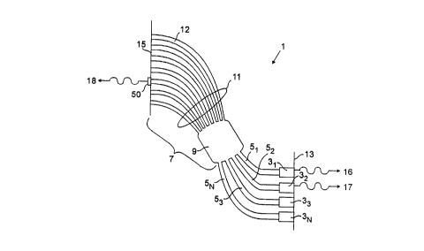
FIG. 1 is a schematic diagram of a digital laser
according to the present invention;
FIG. 2 illustrates the operating principle of the
reflective Dragone router;
FIG. 3 iS a cross section through a digital laser
according to the present invention; and
FIG. 4 illustrates the spectral results observed at
a port of a digital laser according to the present
invention.
DETAILED DESCRIPTION OF THE lNV~NllON
A digital laser 1 according to the present invention
15 iS illustrated in FIG. 1. The laser 1 comprises a number
of optically active sections 31-N/ also referred to as
optical amplifiers, for providing optical amplification,
a number of waveguides 51-N for carrying optical signals,
and a wavelength selective device 7 for providing
wavelength selectivity.
Each optical amplifier 3 comprises a doped section
of waveguide with controllable optical transmissivity.
The sections defining the optical amplifiers 31-N are
optically active in that application of electrical energy
25 will cause them to become transmissive to the flow of
optical energy and further provide some amount of gain to
optical signals flowing through them. In the absence of
applied electrical energy, these doped sections of
waveguide are substantially opaque to the transmission of
30 light. The specially doped sections thus may be
considered to be optical amplifiers or gates depending
upon whether or not
~ .,
j:
they are activated, i.e., excited with electrical energy
such as a bias current. The doped sections may be formed
using standard techniques well known to those skilled in
the art, including, but not limited to, metalorganic vapor
5 phase epitaxy. A gate control device 4, shown in FIG. 2,
selectively provides bias current to one of the optical
amplifiers 31-N- The design of a gate control device is
well known to those skilled in the art.
The reflective wavelength selective device 7
illustrated in FIG. 1 may be defined on a wafer. The
device 7 comprises a free space region 9 for expansion of
the signal from one of the waveguides 51-N' and a waveguide
grating 11 comprised of waveguides or grating arms 12.
The number, N, of waveguides 51-N does not necessarily
correspond to the number of grating arms 12 in the grating
11. Typically, there are more grating arms in the grating
11 than waveguides 51-N' SO that the number, M, of grating
arms 12 is greater than N, or M > N. The ratio of M to N
is usually about 3, but this value is not preferred over
2 O others.
The digital laser 1 further includes two cleaved
facets or surfaces 13 and 15 which comprise high
reflection mirrors defining a cavity in which lasing
action can be supported.
The waveguides 51-N containing optical amplifiers 31-N'
the wavelength selective device 7 and the cleaved surfaces
13, 15 may be monolithically integrated on a semiconductor
wafer using techniques known to those skilled in the art.
The plurality of optical amplifiers 31-N connect one
end of the waveguides 51-N to the first cleaved surface 13.
There is a preferably a one to one correspondence between
the number of waveguides 51-N and the number of optical
amplifiers 31-N- The waveguides 51-N are connected, at
their other end, to the free space region 9. The free
space region 9 is also connected to the plurality of
~ J
grating arms 12 which form grating 11. As mentioned
above, the grating 11 and the free space region 9 comprise
the wavelength selective device 7. The grating 11
terminates at the second cleaved surface 15. For a non-
tunable laser, only one optical amplifier 3 and onewaveguide 5 is used in conjunction with the wavelength
selective device 7.
The overall operation of a tunable laser 1 may be
summarized as follows. Selectively applying electrical
energy, such as a bias current, through the gate control
device 4, to one of the optical amplifiers 31-N will create
certain wavelength selective optical pathways between the
cleaved facets 13 and 15 due to the behavior of the
wavelength selective device 7. Optical energy,
spontaneously emitted from one of the amplifiers 31-N'
travels along the waveguide associated with the emitting
amplifier. As illustrated in FIG. 2, the emitted optical
energy or signal 60 emitted from an optical amplifier 32~
for example, when excited by a bias current, is comprised
20 of a plurality of spectral components 61, 63, 65, 67 of
differing wavelengths ~ 2~ ~3~ ~n It should be
understood that the signal will have more than four
spectral components, so that component " 67 " is intended to
represent the "Nth" component. The signal 60 expands in
25 the free space region 9 so that the signal 60 enters each
of the grating arms 121 M. The signal 60 travels along the
grating arms until it reaches the facet mirror 15. Upon
contact with the mirror 15, the light is reflected back
along the grating arms and reenters the free space region
9. The grating arms 121~ introduce a phase delay between
the spectral components 61, 63, 65, 67 causing the
components to couple to different waveguides 51-N For
example, spectral component 65, having a wavelength ~3,
might couple to the waveguide 53. After coupling to the
3 5 appropriate waveguides 51-N' the individual spectral
~13~
g
components propagate to the optical amplifiers 31-N. Since
only one amplifier is biased, amplifier 32 in FIG. 2, the
remaining amplifiers absorb any light reaching them. So,
if spectral component 65 coupled to waveguide 53, it would
5 be absorbed in the optical amplifier 33 since only
amplifier 32 is biased in the present example.
Thus, by biasing only one of the amplifiers 31-N~ a
specific transparent route between the mirrors 13, 15 for
lasing action is defined, which route supports propagation
10 of light of a specific wavelength. Stationary waves can
be sustained only for wavelengths within a passband
associated with this route. Wavelengths outside of this
passband are suppressed by the lossy unbiased optical
amplifiers. Lasing occurs at the Fabry-Perot mode whose
15 wavelength is nearest the passband maximum. Adjacent
Fabry-Perot modes are suppressed by passband selectivity
which can be adjusted by appropriate circuit design.
There are N passbands ~ wide repeated periodically with a
free spectral range (FSR) period N~. Assuming that the
20 gain of the active semiconductor medium peaks sufficiently
over one of these FSRs, N lasing wavelengths can be
obtained in this FSR by activation of selected optical
amplifiers 31-N. Wavelengths outside this FSR are
suppressed by gain discrimination. Tuning can ~hus be
25 achieved at discrete wavelengths separated by intervals
over a tuning range N~
The details of construction and operation of
transmissive wavelength selective devices are more fully
described in Dragone et al., suprai Zirngibl et al.,
30 "Demonstration of a 15x15 Arrayed Waveguide Multiplexer on
InP," IEEE Photon. Tech. Lett., 4(11) at 1250-53 (1992);
Zirngibl et al., "Polarisation Independent 8x8 Wavegide
Grating Multiplexer on InP," Elect. Lett., 29(2) at 201-02
(1993) and U.S. Patents 5,002,350 and 5,136,671. The
35 reflective wavelength selective device may be formed by
- lo - ~ 3 5
cleaving such transmissive wavelength selective devices
into two pieces, preferably of equal size.
Described below is an example illustrating how the
laser of FIG. 1 may be tuned to a plurality of discrete
optical wavelengths. If it is desired that the laser of
FIG. 1 produce optical energy at a wavelength A1, bias
current is applied to optical amplifier 31. The bias
current applied to the optical amplifier 31 is above the
lasing threshold for the semiconductor material. An
optically transmissive path is thereby defined between
the reflective surfaces 13 and 15 comprising the optical
amplifier 31~ the waveguide 51~ and the wavelength
selective device 7. An optical standing wave is created
between the mirrors 13 and 15 at the wavelength A1, and
laser light at that wavelength may be emitted by the
device from mirror 13 at reference numeral 16. In such a
case, the mirror 13 may be partially transmissive, for
example, 80 percent reflective, while face 15 may be
substantially totally reflective, for example, 98 percent
reflective. A coating (not shown) may be added to the
~acet mirror 13 so that it will be more reflective than a
non-coated facet mirror, yet still be partially
transmissive. A high reflection coating (not shown) may
be applied to facet mirror 15 so that it will be highly
reflective. Such coatings are well known to those
skilled in the art.
Similarly, if it is desired that the laser 1 of
FIG. 1 produce optical energy at a wavelength A2, bias
current is applied to the optical amplifier 32. Again,
the bias current applied to the optical amplifier is
above the lasing threshold for the semiconductor
material. An optically transmissive path is thereby
defined between the faces 13 and 15 comprising the
optical amplifier 32, the
3 ~
waveguide 52 and the wavelength selective device 7. An
optical standing wave is created between the faces 13 and
15 at the wavelength ~2 and laser light at that wavelength
is emitted by the device of FIG. 1 at reference numeral
17. Optical energy at wavelengths ~3 to ~N may be
produced by activating optical amplifiers 33 to 3N~
respectively, instead of activating the optical amplifiers
31 or 32. The operating wavelength of the laser of FIG. 1
may rapidly be changed by biasing a different optical
amplifier.
In a preferred embodiment, the mirrors 13, 15 may be
appropriately coated so that the mirror 13 is
substantially totally reflective and mirror 15 is
partially transmissive, so that light is emitted by the
device at mirror 15. In a most preferred embodiment, a
single output port 18 is provided for light of any
wavelength at mirror 15. In this case, mirrors 13 and 15
are highly reflective except at the output port 18 which
is associated with one of the grating arms 12. At the
output port 18, the mirror 15 is coated with an anti-
reflection material 50 so that it is substantially
transmissive. There is presently no preference as to
which grating arm is selected for location of the output
port 18.
A laser according to the present invention has been
produced and tested. A reflective lx7 Dragone router,
formed by cleaving a transmissive lx7 Dragone router, was
used as the wavelength selective device 7, which
demultiplexes seven equally spaced wavelength channels.
The path length difference between adjacent grating armsis 61.46 micrometers. A cross section through the laser
is shown in FIG. 3. The left side of FIG. 3 illustrates
the semiconductor structure of a section of the active
waveguide 51-N doped to create an optical amplifier
suitable for use in the present invention. The right side
~3~
- 12 -
of FIG 3 illustrates an undoped section of passive
wavegulde.
The epitaxial growth and regrowth for the device were
accomplished by low pressure (100 torr) metalorganic vapor
phase epitaxy. Indium phosphide (InP) was used as the
substrate 19. Any substrate suitable for laser
fabrication may be used, including, but not limited to,
InP or gallium arsenide (GaAs). The substrate was S-doped
(2xlOlB/cm~3). The rib waveguide structure 20 was formed
from InGaAsP. The waveguide region 20 provides
waveguiding in the vertical direction while region 29
provides lateral waveguiding. The amounts of the Group
III organometallics and the arsine were varied to form a
continuously graded region to cover a 1.1 to 1.35
micrometer band gap. To produce the active region of the
laser cavity (the optical amplifier), 1.58 micrometer
InGaAsP quantum wells 21 and 1.35 micrometer band gap
InGaAsP barriers 22 lattice matched to the InP substrate
24 were used. Diethyl zinc and disilane were the sources
for the p- and n-type dopants. Passive waveguides and
amplifier sections were defined by wet-chemical etching
after the first growth. Then, a semi-insulating InP layer
26 was grown everywhere except on the amplifiers. The
final regrowth, a heavily doped p+ -InP layer 2~ with a p+
-InGaAsP cap, not shown, serves as a contact layer.
Contacts 30 were then metallized and the facets, not
shown, were cleaved and high reflection mirrors were
deposited thereon.
The device was tested by sequentially turning on all
the amplifiers. A fiber microlens was coupled to each
amplifier port and light was directed to a optical
spectrum analyzer. FIG. 4 shows the results of the
spectral analysis of light from the fourth port. The
continuous wave (CW) threshold current was 101.5 milliAmps
(mA). The laser emitted -1.8dBm power for a pump current
~ 3
of 120 mA. The emission wavelength 40 of the laser was
1502.52 nm. The next sets of mades 42, which are one FSR
away, are suppressed by more than 30 db. The background
spontaneous emission, which peaks at reference number 44,
is down by more than 35 dB. For different bias
conditions, the laser emitted on the neighboring modes at
1492.95 nm or 1512.78 nm. Thus, the FSR of the
multiplexer was 9.9 nm and the channel spacing was 2.82
nm. The emission wavelength of the other ports were
consistent with this channel spacing and FSR.
To suppress spurious modes from the laser, a
wavelength selective mirror can be employed and the
optical amplifiers should be designed with a peaked gain
profile.
It should be understood that the embodiments and
variations shown and described herein are illustrative of
the principles of this invention and that various
modifications may occur to, and be implemented by those
skilled in the art without departing from the scope and
spirit of the invention.