Note: Descriptions are shown in the official language in which they were submitted.
21~3922
TITLE OF THE INVENTION
WIDE ASPECT TELEVISION RECEIVER
BACKGROUND OF THE INVENTION
Field of the Invention
The present invention rela.tes to a wi.de aspect
television receiver to reproduce picture images on a wide
screen having an aspect ratio of 16:9 from video signals
with aspect ratio of 4:3, for example.
Description of the Related Art
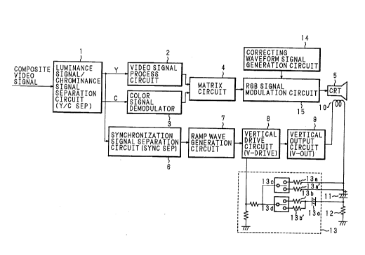
FIG.1 is a block diagram of a part of a wide aspect
television receiver of the prior art. A luminance signal/
chrominance signal separation circuit (Y/C SEP) 1 separates -~
a composite video signal generated by frequency multiplexing
of a luminance signal Y and a chrominance signal C back into
the Y signal and the C signal, outputs the Y signal to a
video signal process circuit 2 and to a synchronization
signal separation circuit (SYNC SEP) 6, and outputs the C
signal to a color signal demodulator 3. The video signal
process circuit 2 controls the picture quality, contrast and
brightness of the Y signal, and outputs the resultant signal
to a matrix circuit 4. The color signal demodulator 3 ~-
controls the hue and color density of the C signal to gener-
ate a color difference signal and outputs the signal to the
matrix circuit 4. The matrix circuit 4 generates primary
~. ." ".. , ~,,,, .;, ,. ,, , , , , . . , , ~
''''~ ..':; ''''''' ' . ,: . ''
: .:. . .: . . '
2133922
color signals of red, green and blue (~GB) from the lumi-
nance signal Y received from the video signal process
circuit 2 and the color difference signal received from the
color signal demodulator 3. A CRT 5 correctly directs
electron beams, which are controlled according to the RGB
signals, on the red, green and blue phosphors provided on a
fluorescent screen, and thereby reproduces color images.
The SYNC SEP 6 extracts synchronization signals from
the Y signal, and outputs a vertical synchronization signal
~V-SYNC) among the synchronization signals to a ramp wave
generation circuit 7. The ramp wave generation circuit 7
generates a sawtooth wave synchronized with the V-SYNC and --
outputs the sawtooth wave to a vertical drive circuit (V-
DRIVE). The V-DRIVE 8 amplifies the voltage of the sawtooth
wave and shapes the waveform, then outputs the wave to a
vertical output circuit (V-OUT) 9. The V-OUT 9 amplifies the
power of the sawtooth wave and supplies the sawtooth current
to a vertical deflection coil 10 which deflects the electron
beams vertically on the screen. A vertical deflection
linearity correction circuit 13 is provided in a negative
feedback loop where the deflection current is negativelY fed
back to the V-DRIVE 8 in order to correct the linearity of
the sawtooth current, and corrects the sawtooth current to
be uniformly linear or partially nonlinear, depending on the
aspect ratio of the screen where the pictures are to be
,'~ .
2~33922
displayed. Description of circuits of the horizontal deflec-
tion system will be omitted here~
The vertical deflection linearity correction circuit 13
is composed of two pairs of feedback resistances 13a, 13a' (
resistance value: 13a > 13a') and feedback resistances 13b,
13b' (resistance value: 13b > 1-3b'), a switching circuit 13c
to switch over the feedback resistances 13a and 13a' accord-
ing to the aspect ratio of the screen whereon to reproduce
pictures, and a switching circuit 13d to switch over the '
feedback resistances 13b and 13b' according to the aspect
ratio of the screen. The feedback resistances 13a, 13a' are
connected in parallel to the positive lead of a coupling
capacitor 11 of which negative lead is grounded via a ~ ;
feedback resistance 12, while the feedback resistances 13b,
13b' are connected in parallel to a lead wire which connects
the negative lead of the coupling capacitor 11 and the ~-
feedback resistance 12, via a coupling capacitor 13e.
"Direct current component DC + alternate current component
AG" is negatively fed back from the positive lead of the
coupling capacitor 11, and the alternate component AC is
negatively fed back from the negative lead of the coupling
capacitor 11, via the vertical deflection linearity correc~
tion circuit 13 to the V-DRIVE 8. ~-
By the switching circuits 13c, 13d of the vertical
deflection linearity correction circuit 13 switching over
, . .... ~ .
21 33922
the feedback resistances 13a, 13a' and the feedback resist-
ances 13b, 13b', respectively, a raster is formed by a
sawtooth current uniformly linear over the entire screen in
the vertical direction when reproducing pictures on an
ordinary screen, or a raster contracted at the top and
bottom thereof is formed while maintaining the aspect ratio
(circularity) of the ordinary screen at the center of the
screen as shown in FIG.2, by a linear sawtooth current for
the center of the screen and by a nonlinear sawtooth current
for the top and bottom of the screen when reproducing
pictures on a wide screen.
Now the operation of switching over ordinary screen
reproduction and wide screen reproduction by means of the
vertical deflection linearity correction circuit 13 will be
described below. Because the vertical deflection linearity
correction circuit 13 is arranged in the negative feedback
loop of a negative feedback amplifier, an increase in the
amount of feedback leads to a smaller output and a decrease
in the amount of feedback leads to a greater output. By
making use of this characteristics, the switching circuit
13c switches to the feedback resistance 13a' of a lower
resistance value when reproducing pictures on a wide screen.
Consequently, an inversely parabolic output as shown in
FIG.3A lS obtained because higher parabolic voltage in one
vertical scanning period is fed back than that in ordinary
.: . ' . . , ., ~, , .
~ ~ . .. .
.. :,,. . : . . ~ .
~/..,, ,~ ..: ~
--' 21 3~g~2
screen reproduction. Therefore, such a vertical deflection
current flows in the vertical deflection coil 10 as to form
a raster expanded at the top and contracted at the bottom.
The switching circuit 13d also switches over to the
feedback resistance 13b' of a smaller resistance value. At
this time, because more differentiated sawtooth wave ob~
tained in the coupling capacitor 13e is fed back than that
in ordinary screen reproduction, the output is smaller only
at the start as shown in FIG.3B so that such a vertical
deflection current flows in the vertical deflection coil 10
to form a raster contracted at the top. When these two ;~
outputs are synthesized, vertical deflection currents of
portions corresponding to the top and bottom of the screen
are nonlinear as shown in FIG.3C, assuming that there is no ~'
deflection distortion, a raster having good linearity at the
center of the screen and contracted at the top and bottom
thereof is formed as shown in FIG.2. ~ ~
In ordinary screen reproduction wherein a linear ~- -
vertical deflection current over the entire screen is
supplied, the switching circuit 13c and the switching
circuit 13d switch over to the feedback resistance 13a and
the feedback resistance 13b which have higher resistance
value, respectively. Output of the vertical deflection
linearity correction circuit 13 becomes a linear sawtooth
wave as indicated by a broken line in FIG.3C, so that a
2133922
raster having good linearity over the entire screen is
formed.
At the same time, the vertical deflection width is also
switched so that the same over scan in the vertical direc-
tion as shown in FIG.4 can be obtained both in ordinary
screen reproduction and in wide screen reproduction.
With such a constitution as described above, displaying
a picture of aspect ratio 4:3 on a wide screen of aspect
ratio 16:9 hardly causes unusual impression of vertical
contraction.
However, since the wide aspect television receiver of
the prior art displays a picture of aspect ratio 4:3 on a
screen of aspect ratio 16:9 by contracting the raster at the
top and bottom of the screen while maintaining circularity
(aspect ratio) at the center of the CRT screen, only by
means of the vertical deflection linearity correction
circuit 13 which deals with the linearity of vertical
deflection, horizontal scan lines are denser at the top and
bottom where the raster is compressed, resulting in higher
luminance in these portions of the screen.
Besides, the pincushion distortion on the right and
left of the top and bottom of the screen where the raster
being contracted is not properly corrected because when the
raster ls contracted only at the top and bottom after simply
broadening the vertical deflection width wider than that in
,,, ., ~ .....
~ :,; :.' ,, - .
, . . : .
.i ~ , . ..
.. ;- . ..... . ..
~1 3~,922
ordinary screen reproduction, contraction at the top and
bottom results in a relatively greater influence of the
horizontal deflection magnetic field on the top and bottom
portions of the screen.
Especially, when using a CRT of high-definition where
the pitch of the phosphor stripes on the CRT fluorescent
screen or the corresponding pitch is equal all over the
screèn, the unevenness in luminance at the top and bottom of
the screen as described above is conspicuous. -;
SUMMARY OF THE INVENTION --
The present invention has been devised in order to
solve the problems described above. It is an object of the -~ -
invention to provide a wide aspect television receiver
capable of correcting the luminance of the picture at the
top and bottom of the screen where the luminance becomes
higher because the scan lines are denser due to contraction
of the raster at the top and bottom, when an ordinary screen
picture is expanded and reproduced on a wide screen.
It is another object of the invention to provide a wide
aspect television receiver capable of properly correcting
the pincushion distortion on the right and left portions of
the top and bottom of the screen where the raster is con-
tracted when an ordinary screen picture is expanded and
reproduced on a wide screen by contracting the raster at the
2I33~22
top and bottom of the screen.
The above and further ob~jects and features of the
invention will more fully be apparent from the following
detailed description with accompanying drawings.
BRIEF DESCRIPTION OF THE D~AWINGS
FIG.1 is a block diagram of a wide aspect television
receiver of the prior art;
FIG.2 shows a raster pattern without any deflection
distortion in wide screen reproduction;
FIG.3A is a waveform diagram of a vertical deflection
current passed through a feedback resistance of a lower
resistance value in a first switching circuit 13c;
FIG.3B is a waveform diagram of a vertical deflection
current passed through a feedback resistance of a lower
resistance value in a second switching circuit 13;
FIG.3C is a waveform diagram of a vertical deflection
current outputted from a vertical deflection linearity
correction circuit after synthesizing the waveforms shown in
FIG.3A and FIG.3B;
FIG.4 is a diagram explanatory of overscan in the ver-
tical direction;
FIG.5 is a block diagram of the first embodiment of the
wide aspect television receiver of the invention;
FIG.6 shows a raster pattern without any deflection
. , . . :.
21 33~22
distortion in wide screen reproduction;
FIG.7A is a waveform diagram of a vertical deflection
current passed through the feedback resistance of a lower ~ :
resistance value in the first switching circuit 13c;
FIG.7B is a waveform diagram of a vertical deflection
current passed through the feedback resistance of a lower :~
resistance value in the second switching circuit 13c; :~
FIG.7C is a waveform diagram of a vertical deflection
current outputted from the vertical deflection linearity
correction circuit after synthesizing the waveforms shown in ~ ~ -
FIG.7A and FIG.7B; ~-
FIG.8A is a circuit diagram of an RGB signal modulation ~:
circuit of the wide aspect television receiver shown in
FIG.5;
FIG.8B shows an embodiment of the correcting waveform : ~
signal which is an input to the RGB signal modulator circuit -
shown in FIG.8A;
FIG.8C shows the RGB signal which is an input to the
RGB signal modulator circuit shown in FIG.8A;
FIG.8D shows the RGB signal without correction out-
putted from the RGB signal modulator circuit shown in
FIG.8A;
FIG.8E shows the corrected RGB signal outputted from
the RGB signal modulator circuit shown in FIG.8A;
FIG.9 is a block diagram of the second embodiment of
9 ' '
... ; ~ . ~ ~ - . - :
~?~
-' 2133922
the wide aspect television receiver of the invention;
FIG.10 is a waveform diagram illustrative of another
embodiment of correcting waveform signal used in the wide
aspect television receiver of the invention;
FIG.11 is a circuit diagram illustrative of an
embodiment of a correcting waveform signal generation
circuit of the wide aspect television receiver of the
invention;
FIG.12 is a block diagram of pincushion distortion
correction circuit of the wide aspect television receiver of
the invention;
FIG.13 shows a raster pattern in the presence of
horizontal pincushion distortion in wide screen repro-
duction;
FIG.14A shows an envelope curve of horizontal pulses
~flyback pulses) at point B of the pincushion distortion
correction circuit shown in FIG.12;
FIG.14B is a diagram illustrative of the relationship
between the amount of pincushion distortion correction and
the envelope curve of the horizontal pulses at point B of
the pincushion distortion correction circuit shown in
FIG.12;
FIG.14C shows gate pulses GP supplied to a variable
amplifier of the pincushion distortion correction circuit
shown in FIG.12; and
~;: . . ..
.. .. : , . ;;- , :
, ~:: . : . :: .
., .
.. . .
; 2133922
FIG.14D shows an envelope curve of a current flowing in
the horizontal deflection coil of the pincushion distortion
correction circuit shown in FIG.12;
DESCRIPTION OF THE PREFERRED EMBODIMENTS
Now the invention will be described with reference to
the accompanying drawings. ~:~
Embodiment 1 -~
FIG.5 is a block diagram of a part of the wide aspect
television receiver of the invention. A luminance signal/
chrominance signal separation circuit (Y/C SEP) 1 separates
a composite video signal generated by frequency multiplexing
of a luminance signal Y and a chrominance signal C back into
the Y signal and the C signal, outputs the Y signal to a
video signal process circuit 2 and to a synchronization
signal separation circuit (SYNC SEP) 6, and outputs the C
signal to a color signal demodulator 3. The video signal
process circuit 2 controls the picture quality, contrast and
brightness of the Y signal, and outputs the resultant signal
to a matrix circuit 4. The color signal demodulator 3
controls the hue and color density of the C signal to gener-
ate a color difference signal and outputs the signal to the
matrix circuit 4. The matrix circuit 4 generates primary '
color s1gnals of red, green and blue (RGB) from the lumi-
nance signal Y received from the video signal process .i.
~ : ,
.?~ . ~
2133922
circuit 2 and the color difference signal received from the
color signal demodulator 3, and outputs the primary color
signals to an RGB signal modulation circuit 15.
A correcting waveform signal generation circuit 14
generates a wave which is parabolic in one vertical scanning
period to correct luminance difference on the screen due to
the difference in density of horizontal scan lines in wide
screen reproduction by changing a vertical deflection
current to be partially nonlinear in the vertical deflection
circuit system, and outputs the wave to the RGB signal
modula*ion circuit 15. The RGB signal modulation circuit 15
amplitude-modulates the RGB signal in one vertical scanning
period by the parabolic wave supplied from the correcting
waveform signal generation circuit 14, and suppresses
amplitudes of the RGB signals corresponding to the top and
bottom of the screen within a specified level, thereby
decreasing the luminance at the top and bottom of the
screen. A CRT 5 reproduces color images by correctly
directing electron beams controlled by the RGB signals which
are modulated in the RGB signal modulation circuit 15, on
the red, green and blue phosphors on the fluorescent screen.
The SYNC SEP 6 extracts synchronization signals from
the Y signal, and outputs a vertical synchronization signal
(V-SYNC) among the synchronization signals to a ramp wave
generation circuit 7. The ramp wave generation circuit 7
12
,
.. . .
.", ~ ~. .
~ .
2133922
generates a sawtooth wave synchronized with the V-SYNC and
outputs the sawtooth wave to a vertical drive circuit (V-
DRIVE). The V-DRIVE 8 amplifies the voltage of the sawtooth
wave and shapes the waveform, then outputs the wave to a
vertical output circuit (V-OUT) 9. The V-OUT 9 amplifies the
power of the sawtooth wave and supplies the sawtooth current
to a vertical deflection coil 10 which deflects the electron
beams vertically on the screen. A vertical deflection
linearity correction circuit 13 is provided in a negative
feedback loop where the deflection current is negatively fed
back to the V-DRIVE 8 in order to correct the linearity of
the sawtooth current, and corrects the sawtooth current to
be uniformly linear or partially nonlinear, depending on the
aspect ratio of the screen where the pictures are to be
displayed. Description of circuits of the horizontal deflec-
tion system will be omitted here.
The vertical deflection linearity correction circuit 13
is composed of two pairs of feedback resistances 13a, 13a'
(resistance value: 13a > 13a') and feedback resistances 13b,
13b' (resistance value: 13b ~ 13b'), a switching circuit 13c
to switch over the feedback resistances 13a and 13a' - -~
according to the aspect ratio of the screen whereon to
reproduce pictures, and a switching circuit 13d to switch
over the feedback resistances 13b and 13b' according to the
aspect ratio of the screen. The feedback resistances 13a,
13
, .. .. .... ... . . . . . .
.
.. . .
,. . ~ .
, . .
~133~22
13a' are connected in parallel to the positive lead of a
coupling capacitor 11 of which negative lead is grounded via
a feedback resistance 12, while the feedback resistances
13b, 13b' are connected in parallel to a lead wire which
connects the ne~ative lead of the coupling capacitor 11 and
the feedback resistance 12, via a coupling capacitor 13e.
"Direct current component DC + alternate current component
AC" is negatively fed back from the positive lead of the
coupling capacitor 11, and the alternate component AC is
negatively fed back from the negative lead of the coupling
capacitor 11, via the vertical deflection linearity
correction circuit 13 to the V-DRIVE 8.
By the switching circuits 13c, 13d of the vertical
deflection linearity correction circuit 13 switching over
the feedback resistances 13a, 13a' and the feedback resist-
ances 13b, 13b', respectively, a raster is formed by a
sawtooth current uniformly linear over the entire screen in
the vertical direction when reproducing pictures on an
ardinary screen, or a raster contracted at the top and
bottom thereof is formed while maintaining the aspect ratio
(circularity) of the ordinary screen at the center of the
screen as shown in FIG.6, by a linear sawtooth current for
the center of the screen and by a nonlinear sawtooth current
for the top and bottom of the screen when reproducing
pictures on a wide screen.
~: -, . .. .
~133~22
....
Now the operation of switching over ordinary screen
reproduction and wide screen reproduction by means of the
vertical deflection linearity correction circuit 13 will be
described below. Because the vertical deflection linearity
correction circuit 13 is arranged in the negative feedback
loop of a negative feedback amp-lifier, an increase in the
amount of feedback leads to a smaller output and a decrease -
in the amount of feedback leads to a greater output. By
making use of this characteristics, the switching circuit
13c switches to the feedback resistance 13a' of a lower
resistance value when reproducing pictures on a wide screen.
Consequently, an inversely parabolic output as shown in ~ ~-
FIG.7A is obtained because higher parabolic voltage in one
vertical scanning period is fed back than that in ordinary
screen reproduction. Therefore, such a vertical deflection
current flows in the vertical deflection coil 10 as to form
a raster expanded at the top and contracted at the bottom.
The switching circuit 13d also switches over to the ~
feedback resistance 13b' of a smaller resistance value. At '
this time, because more differentiated sawtooth wave ob-
tained in the coupling capacitor 13e is fed back than that ~; ~
in ordinary screen reproduction, the output is smaller only ''
at the start as shown in FIG.7B so that such a vertical
deflectlon current flows in the vertical deflection coil 10
to form a raster contracted at the top. When these two
: ~ ' '.
213~9~2
outputs are synthesized, vertical deflection currents of
portions corresponding to the top and bottom of the screen
are nonlinear as shown in FIG.7C, assuming that there is no
deflection distortion, a raster having good linearity at the
center of the screen and contracted at the top and bottom
thereof is formed as shown in FIG.6.
In ordinary screen reproduction wherein a linear
vertical deflection current over the entire screen is
supplied, the switching circuit 13c and the switching
circuit 13d switch over to the feedback resistance 13a and
the feedback resistance 13b which have higher resistance
value, respectively. Output of the vertical deflection
linearity correction circuit 13 becomes a linear sawtooth
wave as indicated by a broken line in FIG.7C, so that a
raster having good linearity over the entire screen is
formed.
The correcting waveform signal generation circuit 14
generates the signal being parabolic in one vertical
scanning~period to correct the difference in luminance on
the screen which is caused when the raster is simply
contracted at the top and~bottom by using only the vertical
deflection linearity correction circuit 13 in wide screen
reproduction (FIG.8B). Then the correcting waveform signal
from the correcting waveform signal generation circuit 14
acts upon the RGB signal modulation circuit 15 to amplitude-
16
: . . .
~ . ;
.,~,' .: :; .. '' : :"', ,. ' :
2133922
.
modulate the video signal (FIG.8C) in one vertical scanningperiod. As a result, amplitudes of the RGB signals corre-
sponding to the top and bottom of the screen are suppressed
within a specified level as shown in FIG.8E.
FIG.8A shows a doubly-balanced modulator circuit as an
example of a circuit for amplitude modulation. When the
parabolic signal shown in FIG.8B is inputted to an input
terminal a and the RGB signals shown in FIG.8C are inputted
to an input terminal b, this circuit outputs such RGB
signals from an input terminal c that has been wholly :-
: :.....
amplitude-modulated with the parabolic waveform as indicated
by dotted line in FIG.8E over the entire period of one
vertical scanning period.
; Transistors Ql and Q2 (emitter-coupled) and transistors
Q3 and Q4 (emitter-coupled) constitute a differential
amplifler. The collectors of the transistors Q5 and Q6 are
; connected to the emitters of the transistors Ql' Q2 and of
the transistors Q3, Q4, respectively, to constitute current
sources for the transistor pair Ql' Q2 and the transistor
pair Q3, Q4, respectively. Resistance values of emitter ';
resistances ~l and ~2 of the transistors Q5 and Q6' which
:. ,.. :
determine the magnitudes of the collector currents I5, I6 of ~ '
the transistors Q5 and Q6~ respectively, are set to be
equal. The parabolic voltage which is inputted through the
input terminal a is impressed to the bases of the tran-
17
' ~.
~ . .
2133922
sistors Q2 and Q3. The R (or G or B) signal which is
inputted through the input terminal b is impressed to the
base of the transistor Q5. Because the base of the
transistor Q6 is biased with a constant voltage V1 equal to
the pedestal level which is inputted to the input terminal
b, the transistor Q6 constitutes a constant current circuit
so that the collector of the transistor Q6 draws a constant
current I6. The collectors of the transistors Q2 and Q3 are
connected to the bases of transistors Q7 and Q8 and the
collector of the transistor Q7. The collector of the j ,~
transistor Q8 i~ connected to the ground potential via a
resistance R3 and to the output terminal c. The transistors
Q7 and Q8 constitute a Miller current circuit, while
collector currents I7 and I8 of the transistors Q7 and Q8
are nearly equal to each other (I7 = I8).
Now the basic operation of the circuit shown in FIG.8A
will be described below. When the correcting signal of the
parabolic voltage shown in FIG.8B is not inputted to the
~ input terminal a, each pair of the transistors Q1 and Q2 and
: the transistors Q3 and Q4 which constitute the differential
a~plifier draws the same collector currents I1, I2 and I3,
I4 as follows.
Il = I2 = Is~ 1~2 (1)
I3 = I4 = I6~ 1/2 (2)
I8 = I7 = I2 + I4 = Is~ 1/2 + I6~ 1/2 (3)
" .~ ' ~ ' ' . ' ' :
, '. ' ' . ' ' .
~ ~ ,
~133~22
When I6 is a constant current and the voltage of the
input signal to the terminal b has the waveform as shown in
FIG.8C, the collector current I5 of the transistor Q5
becomes greater than the collector current I6 of the
transistor Q6 in a video period to. Consequently, the
collector current I8 of the transistor Q8 represented by
equation (3) increases in the video period to. In the case
that the resistance value of the resistance R3 connected 1 i.
between the collector of the transistor Q8 and the ground
level is set to a specified value, a signal of the same
waveform is outputted from the terminal c as that of the ..
signal at the terminal b in the video period to. Moreover,
the signal level becomes nearly the same as that of the
signal at the terminal b outside the video period to . -~
(FIG.8D). ;-:
On the other hand, in a situation similar to that
described previously wherein the collector current I6 of the
transi~tor Q6 i9 a constant current, and the voltage of the ~ -
input signal to the terminal b has the waveform as shown in
FIG.8C while the collector current I5 of the transistor Q5
becomes greater than collector current I6 of the transistor
Q6 in the video period to~ the following inequality holds in
case the positive parabolic voltage as shown in FIG.8B is
applied to the terminal a as the correcting signal.
I5 > I6 (4)
19
,, ~ ;,,:, , . .,.. , -; .:
::. . -: , - j .
~ :GC . ~ . .
~133922
namely
I5 = I6 + ~ Io > I6 (5)
where ~ Io represents an increment in the current of the
transistor Q5 arising because the base voltage of the
transistor Q5 is higher than the base voltage (V1 = pedestal
voltage) of the transistor Q6
The collecto:r currents I2 and I3 of the transistors Q2
and Q3 are greater than the collector currents I1 and I4 of
the transistors Q1 and Q4, respectively, because of the
positive parabolic voltage applied to the terminal a,.
As indicated by equation (3~, the absolute value
I A I21 of the increment in the collector current I2 of the
transistor Q2 is greater than the absolute value I ~ I41 of
the decrement in the collector current I4 of the transistor
Q4 because I5 > I6 in the period to.
I21 > I ~ I41 (6)
From these formulas, the collector current I7 of the
transistor Q7 can be expressed as follows.
I7 = collector current of transistor Q2 + collector current
of transistor Q4
= {(Is- 1/2 + ~ I2)} + {(I6- 1/2) - ~ I4}
= (I5- 1/2 + (I6- 1/2) + (~ I2 ~ I4}) ( )
From comparing equation (7) and equation (3), the
collector current of the transistor Q7 increases by A I2 ~
I4 (> 0) because of the positive parabolic voltage which
~133922
is inputted from he terminal a.
Moreover, because the increment of current (~ I2 ~
~ I4) increases as the positive parabolic voltage which is
inputted from the terminal a increases, output signal
voltage given at the terminal c increases. This means that
the output signal voltage given at the terminal c is
amplitude-modulated by the parabolic voltage inputted from
the terminal a in the video period to. As a result, output
signal of the waveform shown in FIG.8E appears across the
resistance R3 connected between the collector of the -~
transistor Q8 and the ground. -~
As is apparent from the signal waveform shown in
FIG.8E, amplitude of the video signal corresponding to the
top or bottom of the screen in the video period t~ decreases
compared to that of the middle of the screen. Besides, the
amplitude change during one vertical scanning period is
similar, as indicated by the dotted line in FIG.8E, to the
parabolic voltage waveform (FIG.8B) which is inputted from
the terminal a.
In this embodiment, though a so-called negative feed-
back amplifier which has specified frequency characteristics
by arranging the vertical deflection linearity correction
circuit 13 in the feedback loop of the vertical drive
circuit is applied to contract the top and bottom of the
raster in the vertical direction, a reference wave con-
21
... , . , .. , . . _ .
~1339~2
tracted at the top and bottom may also be used in the stageof generating the ramp wave in the ramp wave generation
circuit 7.
In Embodiment 1, though the correcting waveform signal
is generated in the correcting waveform signal generation
circuit 14, a parabolic wave just appeared on the positive
side of the coupling capacitor 11 may also be used.
Embodiment 2
FIG.9 is a block diagram of another embodiment of the
wide aspect television receiver of the invention. Components
identical with those of Embodiment 1 are denoted by the same
numerals and description thereof will be omitted. Although
the RGB signals are corrected in Embodiment 1, the Y signal
(luminance signal), for example, is corrected for the sake
of simplification in this embodiment. This embodiment is
different-from Embodiment 1 shown in FIG.5 in that the
parabolic waveform signal from the correcting waveform
signal generation circuit 14 acts on the Y signal modulation
circuit 16 instead of the RGB signal modulation circuit 15
shown in FIG.5 as in Embodiment 1.
Correction may also be applied by superimposing the
correcting wave on a DC control terminal as to DC-control
the contrast by means of a video signal processing IC.
Embodiment 3
Another embodiment of the correcting waveform signal
2133922
., ,J
generation circuit 14 required to realize the wide aspect
television receiver of the invention will now be described
below.
The correcting waveform signal generation circuit 14 of
this embodiment further clips the parabolic voltage (shown ;
in FIG.8B, for example) generated to modulate luminance, at
a specified level, thereby to shape the waveform of grad-
ually rising in the beginning and gradua~lly falling at the
end but flat in the middle with no change in the voltage, as
shown in FIG.10. FIG.11 is a partial circuit diagram of the
output side from the correcting waveform signal generation
circuit 14 to the RGB signal modulation circuit 15 or the Y
signal modulation circuit 16, wherein the parabolic voltage
signal is inputted from the input terminal d to a bias
circuit 30 of an emitter follower circuit, to which is
connected a clip circuit 32 comprising a resistance Ro and a
zener diode 31.
In the correcting waveform signal generation circuit 14
of this embodiment, the emitter follower circuit (bias
circuit 30) applies a bias voltage to the impressed . ~:
parabolic voltage (shown in FIG.8B, for example). By slicing
the output signal voltage from the emitter follower circuit
at a specified voltage level generated by flowing the
required current with the resistance Ro and the zener diode
31 of the clip circuit 32 in the timing with linearity
23
! i . ', ~ . ~ : -
". .,,' '.::i,
~, ,', i,,, ' ~ :
2133922
contraction of the raster at the top and bottom in the
vertical direction as shown in FIG.6, thereby generating the
correcting waveform shown in FIG.10.
Assuming that the starting time of the vertical
deflection as t1, a period of contracting the vertical
linearity at the top of the screen as t1 through t2, a
period of proper linearity at the center of the screen as t2
through t4, and a period of contracting the vertical
linearity at the bottom of the screen as t4 through t5 as
shown in the right portion of FIG.6, then such a correcting
waveform corresponding to the linearity of each portion is
generated in such timing that the correcting waveform
gradually rises in the period t1 through t2, flat in the
period t2 through t4 and gradually falls in the period t4
through t5 as shown in FIG.10.
Embodiment 4
FIG.12 is a block diagram of a pincushion distortion
correction circuit which corrects the lateral pincushion
distortion at the top and bottom of the screen, namely the
distortion of the vertical lines at the top and bottom as
shown in FIG.13, a.nd is included in the horizontal deflec-
tion system. The pincushion distortion at the right and left
of the screen is corrected to compensate for the insuf-
ficient amplitude at the center of the screen by amplitude-
modulating the horizontal daflection current with the
24
, , : ., ~
~133922
parabolic current having parabolic waveform in one vertical
scanning period. However, in wide screen reproduction, when
the raster is contracted at only the top and bottom after
simply broadening the vertical deflection width to be wider
than that in the ordinary screen reproduction, the pin- -
cushion distortion at the right-and left of the top and
bottom of the screen where the raster is contracted is not
properly corrected because contraction at the top and bottom
results in a side effect of relatively strong influence of
the horizontal deflection magnetic field on the top and
bottom. Therefore, the pincushion distortion correction
circuit of the invention corrects the over-correction of the
lateral pincushion distortion at the top and bottom of the
screen where the raster is contracted.
A drive pulse (HSv) of a specified pulse length
corresponding to a horizontal scanning period and synchro-
nizing with a horizontal synchronizing signal is inputted to
the base of an emitter-grounded horizontal output transistor
28. The collector of the horizontal output transistor 28 is
connected to a positive electrode of a power source VB via a
primary winding 4a of a flyback transformer 27, while a
negative electrode of the power source VB is grounded. The
collector of the horizontal output transistor 28 is grounded
via a series circuit of a capacitor C10 and a capacitor C11.
The collector of the horizontal output transistor 28 is also
~ '''.' ~' ~ .
~i'''' ' '
2133922
grounded via a series circuit of a diode D1o of which
cathode is connected to the collector of the horizontal
output transistor 28 and a diode D11 of which cathode is
connected to the anode of the diode D1o.
The node of the capacitors C10 and C11 and the node of
the diodes D1o and D11 are connected in common. One end of a
secondary winding 4b of the flyback transformer 27 is
connected to the anode of a diode D12, and is connected to a
secondary terminal of the CRT not shown in the drawing via
the diode D12. Another end of the secondary winding 4b is
connected to a positive electrode of a power source VO. The
negative electrode of the power source V0 is grounded.
A vertical deflection sawtooth voltage Vsv is
inputted to a positive input terminal (+) of a vertical output
amplifier 22 via an inverter circuit 21. An output terminal
of the vertical output amplifier 22 is grounded via a series
circuit of the vertical deflection coil 10, the coupling
capacitor C12 and the resistance R1o. A quasi-parabolic
voltage provided at the node of the vertical deflection
coil 10 and the coupling capacitor C12 is inputted either to an
adder 24 via a low-pass filter LF or directly inputted to an
integrator 19.
The sawtooth voltage at the node of the coupling :-
capacitor C12 and the resistance R1o is input to the adder
24 via ~he resistance R11. An output from the adder 24 is
26 ' ~:
~ .. ., . , .,,, .. , ~ ., .
;-, ., . ~ ,. ~, : . : i . .
~.. - ~ .. ." .,, -, . -.- .- :
,.i - :. ,, . ., .. - . - :
, . : . -: , . -
:' :
-' 2133922
inputted to a negative input terminal (-) of the vertical
output amplifier 22. A parabolic voltage outputted from the
integrator 19 is inputted to a variable amplification
circuit 23 which has different gains in a period (t1 through
t2, t4 through t5) during which a gate pulse GP (enclosed by
alternate dot and dash line of ~FIG.12) is at high level and
in a period (t2 through t4) during which GP is at low level.
The parabolic voltage outputted from the integrator 19 is
also outputted to the input terminal a of the RGB signal
modulation circuit 15 shown in FIG.8 or to the input
terminal d of the correcting waveform signal generation
circuit 14 shown in FIG.11. The output voltage amplified by
the variable amplification circuit 23 is inputted to the
base of the emitter-grounded transistor 29 for the diode
modulator. The collector of the transistor 29 is grounded
via the capacitor C13 and is connected to one end of the
primary winding 4a of the flyback transformer 27 via a
series circuit of a diode modulator coil 18, horizontal
linearity coil 25 and a horizontal deflection coil 26. ..
The node of the diode modulator coil 18 and the
horizontal linearity coil 25 is connected to a common node
of the diodes D1o and D11 via the capacitor C14. The
capacitor C10, the diode D1o and the horizontal deflection
coil 26 constitute a first resonance circuit 100, while the
capacitor C11, the diode D11 and the diode modulator coil 18
27
, . . .
~ .
2133922
constitute a second resonance circuit 200.
Now the operation of the pincushion distortion correc-
tion circuit will be described below.
The vertical deflection sawtooth voltage VSV inputted
to the vertical output amplifier 22 causes the quasi-
parabolic voltage, which is linear at the rising portion of
the wave, to be generated at a positive terminal (+) of the
coupling capacitor C12, namely the node of the vertical
deflection coil 10 and the coupling capacitor C12. The
~uasi-parabolic voltage is inputted to the integrator 19
which integrates the inputted quasi-parabolic voltage to
curve the linear portion and generates the parabolic
voltage, while the parabolic voltage is inputted to the
variable amplification circuit 23. In case that the vertical
deflection current shown in FIG.7C flows in the vertical
deflection coil 10 at this time, the distortion on the right - ~
and left sides of the picture at the top and bottom of the - -
screen is excessively corrected so that the vertical lines
curve inward at the top and bottom of the screen as shown in
FIG.13 when displaying, for example, a cross pattern signal
on the CRT.
This distortion is corrected in a process as will be
described below. In the periods t1 through t2 and t4 through
t5 in FIG.6 when the vertical deflection width is
contracted, namely in the periods when the vertical :' :
28
2133922
linearity is contracted at the top and bottom of the screen,
the gain by the variable amplification circuit 23 is
increased in a period during which the gate pulse GP,
repeated by the vertical scanning cycle, is at high level
indicated in an area enclosed by the alternate dot and dash
line in FIG.12. By this operation, the difference in voltage
level between the center and both sides of the parabolic
wave, namely curvature of the parabolic wave, which is to be
the reference wave of the pincushion distortion decreases,
thereby corrects the over-correction of the distortion at
the right and left of the screen. As a result, the inward
curving of the picture at the top and bottom of the screen
described previously is corrected.
The operation of avoiding the excessive pincushion
distortion will be described below in more detail.
FIG.12 shows the constitution of the horizontal
pincushion distortion correction circuit of diode modulator
type, wherein the horizontal output is separated by two
diodes Dlo and D11, and two loops where a sawtooth current
of the horizontal scanning period flows are formed; the one
loop connected to the first resonance circuit 100 comprising
the capacitor ~10' the diode Dlo and the horizontal
deflection coil 26 and the other loop connected to the
second resonance circuit 200 comprising the capacitor Cll,
the diode Dll and the diode modulator coil 18. Because the
29
. .
. .
" :
.' .
~'~ .
2133922
collector of the diode modulator transistor 29 is connected
to the diode modulator coil 18, the current flowing in the
loop connected to the second resonance circuit 200 (lower
loop) is controlled by the output signal from the variable
amplification circuit 23, thereby causing the current
flowing in the loop of the first resonance circuit 100
(upper loop) to be controlled. This means that decreasing
the current in the lower loop causes the current in the
upper loop to increase. The output signal from the variable
amplification circuit 23 is the parabolic signal whose
curvature, namely the difference in voltage level between
the center and both ends thereof is changed from that of the
parabolic wave outputted from the integrator 19 due to the
varying gains applied by the variable amplification circuit ~-
23 upon receipt of the high level gate pulse GP in the
periods t1 through t2 and t4 through t5 (FIG.12).
Because the diode modulator transistor 29 receives a
signal from the variable amplification circuit 23, such a
voltage wave to be inverted (inverted parabolic waveform)
appears at a point B of FIG.12. FIG.14A shows the waveform.
As shown in FIG.14A, control of the horizontal width of
the horizontal deflection is carried out by making a DC
level of an output signal from the variable amplification ~ -
circuit 23 adjustable and by changing the level of the
envelope of the inverted parabolic wave at the point B.
2133922
Envelopes af the voltage waveforms of the horizontal
scanning pulses (flyback pulses) at the point B in FIG.12
(hereinafter called the B point voltage waveform) are shown
in FIG.14B in the cases where the amount of correction for
the pincushion distortion is excessive, proper or insuf-
ficient, respectively.
In case that the pincushion distortion correction
circuit is not used, the excessive curvature of the B point
voltage waveform in the periods corresponding to the top and
bottom of the screen causes the horizontal deflection coil
current in the periods to become too much greater than a
specified value, thereby causing an over correction of the
pincushion distortion in these periods. When the curvature
of the B point voltage waveform in the periods corresponding
to that portion is insufficient, on the contrary, the
horizontal deflection coil current in the periods becomes
too small resulting in insufficient correction of the
pincushion distortion in these periods. When the curvature
of the B point voltage waveform in the periods corresponding
to the top and bottom of the scree~ is appropriate, the
horizontal deflection coil current in the periods becomes
the specified value so that proper correction of the
pincushion distortion is achieved in these periods.
Key point of the pincushion distortion circuit of this
embodiment is that the curvature of the parabolic wave is
31
.. .~ . .
, ~
. .
i, .
.,
.~ :
, ~ .
2133922
made adjustable in limited portions of the top and bottom of
the screen which require correction and, at the same time,
the horizontal deflection width is made adjustable by
changing the direct current level of the entire parabolic
waveform. That is, the additional lateral distortion due to
the nonlinear vertical deflection at the top and bottom of
the screen is eliminated as well as the ordinary lateral
pincushion distortion at the center of the screen.
FIG.14D shows the current flowing in the horizontal
deflection coil 26 in correspondence to the B point voltage
waveform, namely the standard waveform of the current
flowing from a point A to the point B in FIG.12.
As this invention may be embodied in several forms
without departing from the spirit of essential character~
istics thereof, the present embodiment is therefore -
illustrative and not restrictive, since the scope of the
invention is defined by the appended claims rather than by
the description preceding them, and all changes that fall ~
within metes and bounds of the claims, or equivalence of ~ -
such metes and bounds thereof are therefore intended to be ;
embraced by the claims.
'' ~, :-' ~ '
. : . ~ . . . : .: . , ~. . . . : ~.,
. :~ ,, . ,.,:: ~ -