Note: Descriptions are shown in the official language in which they were submitted.
~ WO93/216732 1 3 3 9 7 7 P~T/US93/03738
VERTICAL-CAVITY SURFACE-EMITTING
LASER ARRAY DISPLAY SYSTEM
~ROSS-REF~RENCE TO ~ELATXD APPLICATION
5This application is related to our co-
pending application serial No. 07/790,964 entitled
"Visible Light Surface Emitting Semiconductor ~aser"
filed on November 7, l99l, which is incorporated
herein by reference.
FIELD OF THE INVENTION
The present invention relates to the fie'Ld
of miniature visual display~ and, more particularly,
to miniature visual displays that utilize visible
emitting vertical-cavity surface-emitting lasers ~-
(VCSELs) to project a display within an observer's
field of view. :
BACKGROUND OF T~E INVENTION
Because of the human visual sensory system's
enormous capacity to absorb and process information,
visual displays are extremely effective in displaying
a variety of information formats, such as, for
example, moving sceneries, alphanumeric characters,
~5 maps, graphs, and targeting data, all of which may b
superimposed on an ohserver's normal field of vision.
Particularly, tactical military operations requiring
highly complex series of tasks to be performed in
unpredictable environments greatly benefit from the
30 use of miniature visual displays, such as head-up,
direct view, or helmet-mounted displays. For
instance, tactical aircraft personnel are now being
equipped with helmet-_ounted displays (HMDs) which
allow a miniature visual display system to be held on
35 the head of the observer so as to project a display
W093/21673
2 1 3 :~ 9 ~ 7 PCr/US93/0373~
- 2 -
within the observer's field of vision. In the
commercial sector, high-resolution HMDs can provide a
"virtual reality" for entertainment and education.
In the last decade, a va~t amount of effort
5 has been expended to develop compact, lightweight
visual displays, such as HMDs. Desirably, miniature
visual displays should efficiently`~eliver an image
generated from the display devic~` typically a cathode
ray tube (CRT), to the observer's field of view with
10 minimal or no distortion. Unfortunately, the progress
made to date in the miniature visual display and, more
particularly, the HMD technology has been primaril'y in
the classical or holographic-optics used in the
imaging or relaying of the image. See, for examplle,
15 J. R. Burley et al., "A Full-Color Wide-Field-of-View
Holographic ~elmet Mcunted Display for Pilot/Vehicle
Interface Development and Human Factors Studies,"
Proceedinas of the SPIE, Vol. 1290, pp. ~-15 (1990).
Very little progress has, in fact, been made
20 in developing compact, high brightness, high contrast,
low power CRTs. Accordingly, the lack of suitable
compact CRTs severely limited the applicability of
miniature visual displays, leading to the development
of miniature display systems which utilized other
25 suitable display devices.
One such display system is disclosed in U.S.
Patent No. 5,003,330, which is incorporated herein by
reference. This display system utilizes a diode array
fixed within a helmet-visor structure. Although these
30 diode arrays perform acceptably in the helmet, they
-- have not been completely satisfactory for displaying
high resolution and/or color display images. Linear
diode axrays and even diode laser arrays required to
achieve such improvements are either not availa~le at
35 the desired visible wavelengths for color display
... -.;~.. ... . ..... ....... . ..... .. ..
W~93~21673 PCT/US~3/03738
_ 3 æ 1 3 3 9 7 7
images or not available in the array sizes required
for color or high resolution miniature visual display
applications.
Further, prior art lasers are not suitable
5 for two-dimensional array fabrication or micro-optic
integration which is preferred for today's scanning,
printing and display applications. This is due to the
astigmatic beam quality of conventional semiconductor
lasers as well their high divergence whirh make it
10 prohibitively difficult to project high resolution
imagPs within the field of view of the observer
without the use of relatively expensive and bulky
optics.
Other display dev~ces which have also been
15 d~velop~d in an effort to replace the dominant image
display deYice, include, for example, liquid crystal
di~plays (LCDs), AC and DC plasma dis!?lays, thin film
electro-luminescence displays, and vacuum fluorescent
displays. Each of these alternative technologies,
20 however, has fundamental shortcomings, particularly
for addressing HMD applications. LCDs, for example,
have a very low ~fici~ncy in generating, modulating,
and transmitting light . See, for example, D.L. Jose
et al., "An Avionic Grey-Scale Color Head Down
25 Display,'C Proceedinqs of the 5PIE, Vol. l289, pp. 74-
98 (l9g0). ~lasma displays, on the other hand,
require on the order of approximately l00 volts or
more, while the other alternative display devices are
difficult to scale down to sizes achievable with
30 either the diode or laser array (approximately 20-40
~m2 per element) technology necessary to achieve
miniaturization.
To date, therefore, the size, nature and/or
availability of wavelengths for display devices have
W O 93/21673 .Pt~r~US93/03738
.
213~977 - 4 ~
limited the practicality and utility o~ miniature
visual displays.
It is therefore an object ~f the present
invention to provide a visual display system that
5 utilizes compact, solid state, high efficient, high
brightness, and high contrast display devices for
providing monochrome as well as full color displays to
an observer's field of view. -
It is a further object of the presentinvention to provide a miniature visual display system
that provides a high resolution color image of visual
i~formation and is suitable for a broad range of
consumer, industrial, busine~s, medical and military
applications.
It is still a further objeet of the present
invention to provide a miniature visual display system
or technology that is compatible with the existing
classical and holographic optics and which utilizes a
display device that is superior to the prior art
20 display devices to achieve a higher resolution.
SUMM~RY OF THE INV~ENI'ION
These and other objects are achieved in
accordance wit~ the invention in a miniature visual
25 display 5yste~ ~hat utilizes visible laser diode
arrays (VLDAs) and, more preferably, that utilizes
one- and/or two-dimensional arrays of visible emitting
vertical-cavity surface-emittiny lasers (VCSELs) in
order to provide a desired visual display within an
30 observer's field of view.
In preferred embodiments, sweep and sub-
scanning techniques, individually or in combination,
are employed to create a full M x M image from l x N
or N x N arrays of VCSELs, where M is a multiple
35 integer of N. Such scanning techniques advantageously
W093/2~673 2 1 ~ 3 9 7 7 PCT/US93/0373X
further increase the resolution of the displayed image
for a given number of VCSELs by displacing the image
of the VCSELs within the field of view of the observer ~-
as the VCSELs are simultaneously modulated with the
5 information ~o be displayed.
Preferably, the VCSELs are contained within
a display housing which may be attached to the head of
the user by an attachment mechanism or alternatively
may be hand held or mounted. Advantageously, the
10 circular symmetry and low divergence of the emitted
VCSEL radiation as well as ~he availability of
multiple wavelengths, particularly, red, blue and
green, allow high resolutio~ monochrome or color
images to be generated. Addressing individual VCSELs
within two-dimen~ional arrays is achieved by utilizing
matrix addressing techniques, such as by the use of a
row/column addresæing geometryO
BRIEF DES~RIPTION_OF THE DRAWING
A more complete understanding of the
invention may be obtained by reading the following
description in conjunction with the appended drawings
in which:
Fig. l is a cross-sectional view of a
25 visible emitting vertical-cavity surface-emitting
laser ~VCSEL);
Fig. 2 is an exemplary VCSEL array display
system in accordance with the principles of the
inventlon;
Fig. 3 is another exemplary VCSEL array
display system illustrating the use of full-sweep
scanning;
Fig. 4 is an illustration of the effective
beam positions seen by an observer viewing into the
35 VCSE~ array display system of Fig. 3;
WO93/21673 ~ PCT~US93J0373X
2133977 - 6 ,. ~
Fig. 5 is a cross-sectional view of a
monolithically integrated VCSEL array and micro-
lenslets used in the practice of the present VCSEL
array display 8y8tem;
Fig. 6 is an illustra~ion of the effective
beam positions seen by an obserYer viewing into a
VCSEL array display system utilizing sub-scanning
which improves the image resolution;
Fig. 7 is an illustration of the use
10 multiple micro-lenslets with sub-scanning to increase
the effPctive resolution of the display system of the
present invention;
Fig. 8 is a top vi~w of a staggered linear
array of VCSELs with electronic drivers fabricated on
15 a different substrate;
Fig. 9 is illustration of the effective beam
positions s~an by an observer viewing into a one-
dimensional VCSEL array system utilizing jump
scanning;
Fig. lO is an illustration of the effective
beam positions seen by an observer viewing into a
VCSE~ array display system utilizing ~weep scanning in
conjunction with sub-scanning;
Fig. ll is a top view of Zl ultra-wide field-
25 of-view helmet mounted display in accordance with the
invention; and
Fig. 12 is a side view of the helmet mounted
display of Fig. ll.
DETAILED DESCRIPTIQN
The present invention is based on utilizing
visible emitting yertical-cavity surface emitting
asers (VCSELs) to develop a high brightness, high
efficient, compact display technology and, more
35 specifically, a VCSEL array display system.
WO93/21673 2 1 ~ 3 9 7 7 PCT/~S93/03738
-- 7
Particularly, the size, structure and nearly-ideal
beam qualities of the VCSEL~ afford high resolution
monochrome or color display images, real or virtual,
to be placed within an observer's field of view.
VCSELs are a new class of semiconductor -
lasers which unlike conventional edge-emitting laser
diodes emit laser radiation in a direction
perpendicular to the plane of the p-n junction formed
therein. As disclosed in our co-pending application
10 serial No. 07/790,964, VCSELs may now ~e fabricated to
emit visible laser radiation in the range between 0.4
and 0.7 ~m by utilizing an active quantum well reg:ion
llO comprising alternating l~yers of, for example,
GaInP and Al~Ga~InP which are sandwiched between two
distributed Bragg reflectors (DBRs) or mirrors 120 and
130, as illustrated in Fig. l.
In operation, injection current is typically
confined within active region llO by the use of
annular shaped proton implanted regions 140 to achieve
20 stimulated emission. Importantly, VCSELs may be
fabricated in one- and/or two-dimensional arrays and
may be integrated with micro-optics~ With the
appropriate s~lection of materials, each VCSEL can be
made to emit laser radiation in different portions of
25 the visible re~ion of the electromagnetic spectrum.
The operation and fabrication of these VCSELs are
discussed in de~ail in the above-identified related
application and will not be described in detail here
for the sake of brevity.
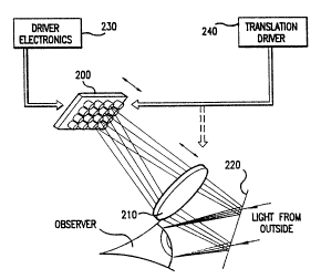
The basic concept of the VCSEL array display
system is illustrated in Fig. 2. Tt is to be
understood, however, that the VCSEL array display
system depicted in Fig. 2 is for the purpose of
illustration only and not for the purpose of
35 limitation. The VCSEL array display system, which is
WO93/21673 PCT/US93/03738
."~
'~13397~ - 8 -
typically positioned about the observer~s head, such
as for use as a HMD, comprises an array of VCSELs 200,
a lens system 210, and, preferably, a partially
transmittin~ faceplate 220, such as a dichroic filter
5 or mirror. Lens system 210 isjpl~ced approximately an
effective focal length away from VCSEL array 200 so as
to collimate the visible radiation emitted from VCSEL
array 200 in order to produce a virtual image of VCSEL
array 200 in accordance with well-known optical
10 theoxy. At any instant in time, an observer looking
into faceplate 220 sees simultaneously a virtual image
of VCSEL array 200 as well as external visual
information that is directe~ toward faceplate 220.
In displaying the desired image to the
15 observer, each laser within VCSEL array 200 may be
individually addrecsed and modulated with the
appropriate chroma or monochrome information by driver
electronics ~30. The necessary electrical signals to
address and generate the desired light intensity have
20 very low drive currents and voltagès that are
compatible with analog or digital integrated CMOS and
TTL electronic circuits.
Additionally, three~dimensional virtual
imag~s can be produced by translating VCSEL array 200
25 or, alternatively, lens system 210 alnng the optical
axis of the system to sw~ep the virtual image location
from infinity to a distance close to the observer.
Such translation may be readily accomplished by a
translation driver 240 that utilizes mechanical servos
30 or piezoelectric transducers to physically move the
array or lens.
It is anticipated that the space occupied by
VCSEL array 200 will be approximately the same as that
occupied by the phosphor screens of prior art
35 miniature CRTs, which typically have a dimension of
WO93/21673 2 I 3 3 9 7 7 PCT/US93/03738
~. .
_ 9 _
approximately 20 x 20 mm. Accordingly, critical
parameters such as the HMD's field of ~iew (FOY) and
packaging known in the prior art will remain
s~bsti~ntially unaffected by utilizing VCSEL array 200
5 rather than the conventional CRT or other well known
display devices. Moreover, those skilled in the art
will know of optical designs and packing means which
would further facilitate the use of VCSEL array 200 as
a display system suitable for attachment to the head
10 of an observer or for hand-held use. For example, see
U.S. Patent Nos. S,023,905 and 5,048,077 which are
incorporated hersin by reference. For instance, the
VCSEL array display of the present invention may be
packaged in a disp'ay unit having an opening through
which the image may be ~iewed and may be attached to a
sidewall of a user's helmet, or a user's eyeglasses.
Alternatively, the display system may be attached to a
user's belt, with remote display information pro~ided
from a computer, pocket calculator, or radio wa~e
20 transmitter.
In one embodiment, VCSEL array 200 comprises
a two-dimensional M x M array of individually
addressable VCSELs. VCSELs within the M x M array may
be f abricated to lase either at one predetermined
25 wavelength or at several wavelengths, such as blue,
green and red, to produce monochrome or full color
images, respectively, in arcordance with well known
colorimetry theory.
The VCSEL array is fabricated using
30 conventional planar large scale lntegration (LSI)
- processing techniques, such as _olecular beam epitaxy
(MBE), wet chemical etching and the like. More
particularly, the two-dimensional array is fabricated
by first depositing epitaxially the semiconductor
35 layers of the VCSEL structure and then defining, for
W093/21673 PCT/US93/03738
213397~
-- 10 --
example, by optical photolithography and etching a
plurality of columns, each a separably addres~able
VCSEL. Contacts to the VCSELs are formed by
conventional deposition techni~es wherein, for
5 example, common row and colu~n.~us contacts may be
formed to individually address each VCSEL, as
disclosed in our co-pending application serial No.
07/823,496 entitled "Integra~ion of Transistors With
Vertical Cavity Surface Emitting Lasers" filed on
10 January 21, 1992, which is incorporated herein by
reference.
The number of VCSELs in the two-dimensional
array will, of course, be dependent on the required
resolution as well as the width and length of the
displayed image projected to the observer.
In comparison to edge-emitting lasers, which
are a few hundred microns long by 10 ~m, each VCSEL is
approximately 10 ~m in ~iameter, affording more than
twenty-five ~imes more display elements per unit area
20 than prior art display devices. Importantly, the
emitted radiation has a circular symmetry as well as a
low divergence which allow low numerical aperture lens
system to be employed in generating an enlarged
virtual image of the VCSELs. Also, since the VCSELs
25 have no inherent astigmatism and can be fabricated as
closely-spaced, individually electrically addressable
display elements, it will be apparent to those skilled
in the art that an enhanced resolution may be
achieved.
Information is applied to the VCSELs by
individually addressing each VCSEL through the use
of, for example, a matrix or row/column addressing
contacts similar to those used for charged coupled
device (CCD) arrays. Fully addressing a M x M array
35 of display devices electronically requires M2 leads,
W093~21673 2 1 3 ~ 9 7 7 PCT/US93/03738
which is prohibitively impractical at array sizes much
larger than 16 x 16 (256 leads). Accordingly,
information is applied to the VCSELs by individually
addressing each of the VCSELs through the use of the
5 matrix or row/column addressing geometry, reducing the
number of leads from M2 to 2M. See, for example, M.
Orenstein et al., "Matrix-Addressable Vertical Cavity
Surface Emitting Laser Array," Electronic Letters
Vol. 27, pp.437-438 (1g91), which is incorporated
1O herein by reference. Associated driver electronic.s
230, including, for example, shift registers,
transistors, and the like, used for addressing and
modulating the intensity of~the emitted radiation may
be integrated on the chip or substrate containing the
15 VCSEL array rather than being located external to the
display unit. Such integration further reduces the
number of leads, allowing large arrays, e.g., 512 x
512, to be readily fabricated. ~
If the number of elements in the VCSEL array -
?O matches the required resolution of the displayed
image, no scanning other than the electronic
addressing is necessary. However, to increase the
resolution for given number of VCSELs or to reduce the
number of VCSELs needed to achieve a desired
25 resolution, various scann-ng techniques may be
employed. More particularly, those skilled in the art
will appreciate that scanning allows a full page
display to be created from a much smaller number of
display devices than is necessary to generate the full
30 page display, whether for a real or virtual image.
For example, a M x M display image may be
generated from a 1 x M VCSEL array by utilizing a
technique known as full-sweep scanning. The full page
display is achieved by scanning along one axis the
35 VCSEL's virtual-image position perceived by the
W093/21673 2~3~97~ PCT/Us93/0377`
- 12 -
observer. In this type of scanning, the VCSEL array
comprises a plurality of linearly-aligned VCSELs
having an individual VCSEL or ç ement for each
resolution element along one~àxis~ Resolution
5 elements along the other axi's are provided by the
scanning mechanism discussèd in more detail below.
Referring to both Figs. 3 and 4, a VCSEL
array 300 comprises a single vertical column of VCSELs
represented by the black dots on the left hand side of
10 Fig. 4. Gollimated light output from the array is
directed by a lens 310 to, for example, a vibrating
mirror 320 of an electro-mechanical scanner 330.
Electro-mechanical scanner 330 may be of type
disclosed in ~.S. Patent No. 4,902,083, which is
incorporated herein by reference, in which mirror 320
is vibrated in accordance with control signals from a
s~anner electronics 350. By selectively illuminating
various lasers within VCSEL array 300 at various
points during the vibration of mirror ~20, successive
20 columns of pixels or picture elements, i.e., display
points, will be caused to appear within the field of
view of the observer. These display points are
represented in Fig. 4 by the entire two-dimensional
array of dots, in which the black dots also represent
~5 the image position of radiation from the VCSELs in the
absence of scanning and the stippled dots represent
the additional display points achieved by scanning.
At any instance in time, the observer sees only one
column or vertical line of VCSEL array 300, but
30 because mirror 320 is repetitively oscillated or
scanned in the horizontal direction 50 as to sweep the
apparent location of the vertical line of VCSEL array
300 from one edge of the observer's field of view to
the other, the observer's eye perceives a full screen
35 of information, as depicted in Fig. 4.
WO93/21673 2 1 3 3 g 7 7 PCT/U~93/03738
- -~
- 13 -
Typically, mirror 320 is oscillating at
approximately 100 Hz so as to create the illusion of a
continuous full pagë or M x M image generated ~rom a 1
x M array.
Of course, the vertical line or column~-of
VCSEL array 300 is appropriately modulated or
electrically excited to selectively emit light for
each column within the desired display image. Such
driver electronics may be integrated with the VCSELs.
10 Electronic timing ensures that the proper VCSEL for
each column or vertical line is illuminated at the
correct time during scanning. One example of a
miniature visual display an~, more particularly, a HMD
which utilizes full-sweep scanning is disclosed in
15 ~.S. Patent No. 4,~34,773, which is incorporated -
herein by reference.
The number of VCSELs in the linear array
will be dependent on, for example, the width of the
desired image to be displayed to the-obæerver. In one
20 preferred embodim~nt, for a 1024 x 1024 display,
VCSEL array 300 would ~vntain 1024 linearly-aligned
VCSELs. VCSELs contemplated for use in this
embodiment are approximately 10 ~m in diameter with
approximately a 10 ~m space between each VCSEL.
2~ It is also possible to use sweep scanning
with a VCSEL array which is not linear, such as, for
example, with a quasi-linear or staggered array.
Those skilled in the art will know how to modify the
electronic driver signals to compensate, in this case,
30 for the altered positions of the VCSELs.
Other scanning techniques which may be more
stable are also contemplated. These techniques, for
example, involve the use of micro-optics which is
readily integrated with the VCSEL array. The
35 formation of sub-millimeter diameter lenslets as well
WO93/21673 2 l 3397 ~ PCT/US93/03738
- 14 -
as the formation of waveguides on the substrate
containing the VCSEL array, for example, i~prove the
performance, light efficiency, surface scattering,
wavelength sensitivity and beam divergence of the
5 display, all of which decre,a~es the size, weight, and
complexity of the imaging ~ystems. Fig. 5 depicts an
exemplary monolithic integration of a VCSEL array 510
and micro-lenslets 520 which may be used in the
practice of the present invention to facilitate the
10 use of various other scanning techniques, such as
electro-optic scanning techniques that employ acousto-
optic _odulators (AOMs). Those skilled in the art
will particularly note that~micro-lenslets 520 direct
the propagation of the radiation emitted by the
15 VCSELs, performing some, if not all, of the imaging
functionality of optical lens 310. For instance,
micxo-lenslets 520 can decrease the beam divergence of
the emitted radiation so that lower numerical aperture
optical systems can be used for displaying a desired
20 image within the field of view of the ob~erver.
Alternatively, they can increase the beam divergence
to increase image resolution.
In another embodiment, a noYel sub-scanning
technique is employed to create a full ~ x M display
25 image from a N x N array of VCSELs, where M is a
multiple integer of N. Sub-scanning, in contrast to
sweep scanning, is the real or virtual movement of the
VCSEL array within the field of view of the observer
by a distance smaller than the inter-element or VCSE~
30 spacing. Referring to Fig. 6, the solid black dots
indicate the position of the image elements of the
VCSELs when directly imaged to the observer. When
each image element displayed to the observer is
scanned along horizontal and vertical axes 610 and
35 620, respectively, the image elements are perceived to
W093/21673 2 I 3 3 9 7 7 PCT/US93/03738
- 15 -
be located at those locations represented by the
stippled dots to create the illusion that a full page
is being displayed. As with sweep scanning, the
radiation from the VCSELs is approprîately modulated
5 during the scanning ~f the VCSEL array. The scanning
can also ba accomplished by a real image displacement
using, for example, piezoelectric transducers.
Typically, the inter-spacing distance, l,
between each VCSEL is an integer multiple of the
10 spacing, d, between the generated sub-elements or the
factor by which the resolution has been improved. It
is contemplated that sub-scanning may be achieved by
the use of other means, such-as piezoelectric
transducers, mechanical scanners, acousto-optic
modulators and the like.
These scanning techniques may also benefit
from the use of micro-~ptics as well as benefit from
their integration with the VCSEL array. For example,
typically the ratio o~ the inter-element spacing to
20 its beam diameter is approximately 2:1. The
utilization of micro-lenslets, such as illustrated in
Fig. 5, to focus the radiation output or beamlet from
each VCSEL to a reduced spot size increases the inter-
element spacing to beam diameter ratio.
25 Advantageously, sub-scanning could then be usPd to
increase the effective resolution by generating sub-
pixels between adjacent VCSELs as discussed above. In
contrast, the beam fr~m a light emitting diode cannot
be focused effectively to a reduced spot size.
Rather than utilizing micro-lenslets, larger
lenslets which collect light from multiple VCSELs can
be used in conjunction with the above sub-scanning
techniques. As shown in Fig. 7, lenslet pairs 710 and
720 focus emitted radiation from multiple VCSELs 730a-
35 d to a reduced spot size. Whereas the spacing between
WO93/21673 P~T/~S93/0373~
2~339~ - 16 - ~`
VCSEL pairs 73Qa-b and 730c-d is originally a
distance, a, the spacing after the beamlets traverse
through the lenslets pairs is a much smaller distance,
b. Sub-scanning may now be used to generate sub-
5 pixels between the imaged VCSELs, which sub-pixels are
indicated by the stippled dots. Note that the
demagnification factor realized by lenslet pairs 730a-
b and 730c-d ~hould be an integer number equal to the
number of sub-pixels required to fill the field of
10 view of the observer or the sp~ce between the imaged
VCSEL points. Utilization of a single macro-lens, in
contrast, does not increase the effective resolution.
Although the macro-lens would decrease the spot size,
it would also decrease the inter-element spacing by
15 the same factor. That is, the ratio of the inter-
element spacing to spot diameter remains unchanged.
Utilization-of sub-scanning cannot therefore be used
to increase the resolution to its maximum po~sible
extent where a single micro-lens is employed.
It is to be understood for the above sub-
scanning tec~nique that the scanning le~gths along
each axis do not have to be symmetric. By utilizing
different scanning lengths it is possible ~o generate
in general a M x N array display image from a K x L
25 VCSEL array, where M and N are multiple integers of K
and L, respectively.
As an example of a sub-scanning system, a
128 x 128 VCSEL array with a 40 ~m inter-element
spacing may be scanned in increments of 5 ~m up to the
30 maximum distance of 35 ~m in both axes to achieve a
1024 x 1024 image (7 sub-positions in each axis
between adjacent VCSEL elements).
In the above embodiments, it is contemplated
that the information to be displayed may initially be -
35 stored in a data storage device such as RAM, ROM,
WO93/21673 2 1 3 ~ 9 7 7 PCT/US93/03738 `
- 17 -
EPROM and the like, which are well known in the art,
when a limited set of information needs to be
selectively provided to the observer. Otherwise, and
for most applications requiring information which
5 varies with time, new information to be displayed may
be applied to the VCSELs during the end of a frame,
such as at the end of a scan.
New information to be displayed may also be
directly applied to each VCSEL to create a full
10 display as discussed above by individually addressing
each VCSEL without the use of matrix addressing.
Furthermore, the N x N VCSEL array may alternatively
comprise rows of VCSELs whic~ are staggered in order
to compensate for gaps between the devices. Fig. 8
15 depicts a portion of a staggered linear array of
~CSELs 810 having wirebonds to electronic drivers 820
which may be fabricated on a different substrate. The
VCSEL arr~y and electronic drivers may alternatively
be fabricated on the same substrate to eliminate the
20 need for wire bonding as disclosed in our pending
application serial No. 07/823,496. Driver electronics
820 include transistors, such as FETs, bipolar ~~-~
transistors, and the like. In general, the structures
disclosed in the above-identified application may be
25 used in the practice of the present invention.
In one example, one-dimensional sub-scanning
may be utillzed for laser printing applications, such
as a 3600 dots-~er-inch (dpi) printer covering a 20 x
75 inch area. A 20 inch linear VCSEL array having 300
30 VCSELs per inch can be sub-scanned in one dimension
such that each VCSEL controls the illumination at 12
points (pixels) in a line to achieve the desired 3600
dpi resolution. Advancing the printing material in
the other dimension allows printing in that dimension.
W O 93/21673 PC~r/VS93/0373~ ~
213~7 - 18 -
An alternative to one-dimensional sub-
scanning is to translate a one-dimensional array of
VLDAs, such as of the VCSEL type, by a distance equal
to a multiple integer length of the array size plus
5 one inter-pixel distance. As shd~n in Fig. 9, a VCSEL
array 850 comprising three gro~ps 860a-c of a 1 x 4
VCSEL sub-arrays is scanne~ by stepping the arrays
through the image in multiple illumination phases. In
the first phase, the arrays control the illumination
10 of display points 870a-c. For the second phase,
radiation from arrays 860a-c is translated, such as by
electro-mechanical means, to the positions indicated
by stippled dots 870a'-c', respectively. The VCSELs
are accordingly modulated with appropriate monochrome
or chroma information corresponding to their
translated positions to generate new effective
re~olution elements or pixels. Then, in the third
phase, radiation from arrays 860a-c is stepped or
translated to positions 870a"-c", respectively. This
20 stepping or "jump" technique effectively produces 4
additionally pixels for each translation or step.
Here, 8 additional pixels are produced for each of
sub-arrays 860a-c. This particular type of scanning,
referred to as "jump" scanning, may also be used for
25 laser printing applications. For example, if 6000
lasers on 60 chips of 100 lasers each would be
required to ac~ieve a desired resolution, then the
same task could be done using 10 chips of 100 lasers
each by performing 6 "jumps" or repeated translations.
Two-dimensional display images may also be
generated by combining both sweep ~canning and sub-
scanning techniques. Referring to Fig. 10, a 16 x 16
display image may be generated from 1 x 4 VCSEL array
by sweep scanning along a horizontal axis 910 and sub-
35 scanning along a vertical axis 920. The inter-element
WO93/21673 ? 1 3 3 9 7 7 PCT/US93/037~ ~
spacing, y, between VCSELs is such that 3 sub-
positions are generated therebetween by displacing the
virtual image of the VCSELs in repeated increments.
Along horizontal axis 9lO the virtual image perceived
5 by the ob~erver is displaced in increments
corresponding to the desired sub-positi.on spacing, x,
up to a distance corresponding to l~ pixels. Along
vertical axis 920, however, the virtual image is
displaced in increments of the desired sub-position
10 spacing, x, but only up to a distance corresponding to
the inter-element VCSEL spacing, y~
A unique aspect of the present invention is
the ability to generate a ful~ color display. In or~e
embodiment of a full-color display, three different
15 types of VCSELs are needed in a single array, each of
which types emits light at a different wavelength such
as a green, blue and red, in order to provide color
visual images. Illustratively, each row of VCSELs in
the array comprises VCSELs of only one type and the
20 colors emitted by such rows alternate in regular
fashion. The rows themselves may be staggered to
eliminate the gaps between each VCSEL.
Under the control of timing and control
circuitry, the appropriate chroma data is applied to
25 each row of VCSETs, but at slightly different time
intervals. As a result, the output from each set of
three adjacent rows of different color VCSELs is
imaged to the same line within the virtual image so as
to produce a color display in accordance with well
3~ known colorimetry theory.
Approximate ranges for the green, red and
blue wavelengths are 6lO-630 nm, 514-554 nm, and 440-
470 nm, respectively. These wavelength ranges
satisfactorily provide the full color spectrum and are
35 within the operating range of the VCSELs disclosed in
WO93/21673 PCT/US93/03738
21339~7 - 20 -
our co-pending application serial No. 07/790,964.
More specifically, alternating layers of GaInP and
Al~Gal~InP within the active region may be used to
generate radiation in the red region; alternating
5 layers of GaInP and Al~Gal~P within the active region
may be used to generate radiation in the green region;
and alternating layers of AlyGal~N and Al~Ga~N within
the active region may be used to generate radiation in
the blue region.
Preferably, 605 nm, 554 nm and 460 nm will
be used as the wavelengths for the red, green, and
blue radiation, respectively, because these
wavelengths provide the highest efficiency for
producing white light. Utilizing longer wavelengths
above 605 nm as the red source requires greater red
light intensity 'n order to maintain the same
irradiance.
Partially transmissive reflectors may
further be used to direct the color display image
~0 within thR field of view of the observer. These
reflectors may be fabricated with enhanced
reflectivities at the radiation wavelengths of the
VCSELs to minimize the required optical power.
Moreover, the reflectivities elsewhere may be
25 minimized (i.e., high transmissivity) to maximize
ou~side ~iewing of external information.
In accordance with the principles of the
invention, VCSELs may be also integrated with, or even
replaced by, other display devices, such as visible
30 diode lasers or superluminescent light emitting diodes
(SLEDs~ to further au~ment and/or complement the
applicability of the present inventive VCSEL array
display system. Those skilled in the art will know
that a SL~D is a light emitting diode (LED) whose
efficiency and emission directionality are enhanced by
WO93/21673 2 1 3 3 9 7 7 PCT/US93/03738
- 21 -
the addition of a partial cavity. SLEDs can be
constructed very similarly to VCSE~s using standard
planar LSI proc~ssing techniques. In accordanc~ with
the principles of inventions, it is cvntemplated that
5 VCSELs will be integrated with SLED and/or LEDs.
In another embodiment, sweep scanning in
conjunction with sub-scanning may further be utilized
to realize a HMD having a ultra-wide field-of-view~
More specifically, the sweep scanning is implemented
10 by using a rotating polygonal mirror to achieve fields
of view near 180 degrees. Rotating polygonal mirro:rs
are advantageously more robust than vibrating mirro:rs
and, moreover, afford one the capability to exploit
the nearly circular symmetry field-of-view of HMDs.
Shown in Figs. ll and 12 are top and side
views, respectively, of a ultra-wide field-of-view HMD
which u~ilizes the principles of the present
invention. Polygonal mirror 920 rotates about a
vertical axis ~o sweep the apparent location of a
20 ~CSEL array 9lO from one edge of the observer's field
of view to the other/ as previously illustrated in
Fiy. 4. A 180 degree field-of-view ~ay be achieved by
a 90-l20 degree rotation of polygonal mirror 920 with
the appropriate number of sides. For this arrangement
25 the VCSEL array advantageously is a linear array
oriented in a vertical direction so that it is
parallel to the axis of rotation of mirror 920. A
cylindrical lens 930 located near the upper portion of
the HMD or forehead of the observer expands the
30 emitted radiation from VCSEL array 9lO along the
horizontal axis. The beam expansion is sufficient to
fill the pupil aperture of both eyes of the observer
to achieve full binocular display. Either an
appropriate horizontal curvature on polygonal mirror
35 920, as shown in Fig. 12, or a multiplicity of
W~93/21673 PCT/US~3/03738
213397~ - 22 -
, ~
cylindrical lenses may, however, be used to replace
single cylindrical lens 930.
It is believed that a vertical expansion of
only 15-~0 ~m need be achieved to account for the
5 observer's head motion. Pre~erably, for binocular
displays, horizontal beam widths of 100 mm or more are
contemplated. A concave partial reflector 940, which
is preferably 50-75 mm from the observer' pupil~,
produces a virtual image of VCSEL array 910 within the
10 field of view of the observer in accordance with well
known optical theory. Appropriately addressing and
modulating each individual VCSEL in conjunction with ~-
sweep scanning then presents~a full panorama display
to the observer.
Note that since radiation from each VCSEL
-traverses through only a small portion of the system,
the system components do not introduce any substantial
optical aberrations. Thus, resolution better than one
cycle per mrad may be accomplished over the entire
20 field-of-view with only a small number of optical
components.
Those skilled in the art will readily note
that the vertical Goncavity of both polygonal mirror
920 and partial reflector 940 is used to tailor the
25 vertical beam characteristics of the emitted
radiation. Cylindrical lens 930 and the horizontal
curvature of concave partial reflector 940, on the
other hand, tailor the horizontal ~hape or beam
characteristics of the emitted radiation. In this
30 manner, the emitted radiation can be properly directed
into, for example, 180 degree fîeld-of-view.
Multiple VCSEL arrays, each array emitting
radiation at a different wavelength can further be
employed to produce color image~. For example, VCSEL
35 arrays 910, 950 and 960 may be placed at different
~_ WO93/21673 2 1 3 3 9 7 7 PCT/US93/03738
t
- 23 -
positions around rotating mirror 920, where array 910
emits red radiation, array 950 emits gr~en radiation
and array 960 emits blue radiation. Radiation from
each array, of course, would be synchronized to
5 generate a color image in accordance with well known
colorimetry theory.
Each side of rotating mirror 920 further
could be tilted vertically with respect to each other
so that each side sweeps out a unique set of
10 horizontal pixels~ For example, with a 4 sided
rotating mirror, each side having a slight vertical
tilt, sub-scanning as described hereinabove may be
realized in the vertical direction to effectively
increase the vertical resolution by a factor of four.
15 Hence, a display resolution of 1024 elements in the
vertical direction could be accomplished by utilizing
a ~ingle array haYing only 256 VCSELs. Note that this
latter scheme effectively combines sub-scanning and
sweep scanning techniques to produce extremely high
20 resolution display images over a ultra-wide field-of-
view with a minimum number of VCSELs.
It should be understood that various other
modifications will be readily apparent to those
skilled in the art without departing from the scope
25 and spirit of the invention. For example, head-down
displays fox cockpit environments may also be
constructed utilizing the principles of the invention
in which a real image is projected from the VCSEL
array onto a screen for viewing by an observer.
30 Moreover, simulators may also be constructed employing
a combination of ~irtual-image and real-image
displays.
Accordingly, it is not intended that the
scope of the claims appended hereto be limited to the
35 description set forth therein, but rather that the
WO93/21673 PCT~US93/03738
213~77 - 24 ~
claims be construed as encompassing all the features
of patentable novelty ~hat raside in the present
invention, including all features that would be
treated as equivalents thereof~b~ those skilled in the
5 art to which this inventio~pertains.
1o ,: