Note: Descriptions are shown in the official language in which they were submitted.
CA 02134008 1998-04-29
'_
ARRAY ANTENNA AND PRODUCTION PROCESS THEREFOR
The present invention relates to an array antenna including non-
linear elements active at a temperature lower than or equal to a liquid nitrogentemperature, and having a frequency transforming means (frequency mixing)
arranged in a form of an array.
In seeking to apply superconductors in electronic devices, it is
important to effectively utilize the low conductivity of the superconductor. Even
in a superconductor having zero direct-current resistance or a superconductor
having a lower resistance compared with a normal conductor, resistance at high
frequency is not always superior to that of a normal conductor. This is because
the high-frequency resistance of the superconductor is proportional to the
square of the frequency, whereas the high-frequency resistance of the normal
conductor is proportional to 1/2 the power at the frequency. In the high-
frequency range, especially at a frequency range higher than or equal to severaltens of GHz, a resistance of a superconductor transfer path becomes sufficientlylarge to be taken into consideration in circuit construction. (see Piel et al., "High
Temperature Superconductors in High Frequency Fields-Fundamentals and
Applications", Proceeding of the 4th International Symposium on
Superconductivity, October, 1991, Tokyo, pp 925). In the case of an
electromagnetic wave received by a patch array antenna, a narrow but long
signal transmission line (hereinafter referred to as the feed line) is employed for
transferring the electromagnetic wave to a signal-detecting portion of the patcharray antenna. In that portion of the antenna, patches serving as antenna
elements are arranged. The total length of the feed line portion is inherently
proportional to the number of the patches provided in the array, increasing the
resistance loss in the feed line portion. Therefore, the signal intensity at thesignal-detecting portion is not increased in proportion to the increased number
of patches, lowering the effectiveness of the array form arrangement of the
patches. There are a plurality of proposals for feeding the signal received by
antennae to the signal-detecting portion while maintaining sufficient signal
CA 02134008 1998-04-29
"._
intensity. In the proposals, it has been proposed to interpose a semiconductor
amplifier at an intermediate position of the feed line or to form the feed line
portion with a superconductor or an optical cable having reduced resistance.
For example, A. Balasubramaniyan, et al., "An Eight MOSFET
Periodic Spatial Power Combiner" 1993 IEEE MTT-S Digest, pp 811, proposes
a feed line construction in which eight semiconductor amplifiers are provided.
On the other hand, in Lewis, et al., "Performance of TlCaBaCuO 30 GHz
Element Antenna Array", IEEE Transaction on Applied Superconductivity, Vol.
3, March, 1993, pp 2844, employment of a superconductor in the feed line
portion has been proposed. Also, Banerjee, et al., "An X-Band Phased Array
Microwave/Photonic Beamforming Network", IEEE MTT-S Digest, pp 505
proposes employment of the optical cable in the feed line.
However, except for the superconductor, it is technically difficult
or even impossible to form several tens or several hundreds of semiconductor
amplifiers within an array antenna. On the other hand, as set forth above, in the
high-frequency range, such as the microwave band, the resistance of the
superconductor becomes substantially equal to or even higher than the normal
conductor, and the benefit of employing the superconductor in the feed line is
lost.
Further concrete discussion of the employment of the
superconductor line proposed by Lewis et al. set forth above will be given
herebelow.
On a 2-inch LaAlO3 substrate, a TlCaBaCuO oxide high
temperature superconductor layer is formed and then the patch portions and
feed lines are patterned. On the back surface of the substrate, a grounding
surface layer of gold (Au) is formed. Sixty-four patches are arranged in an 8 x
8 pattern, with element spacing substantially one-half of the free space
wavelength. Summing of power is made at an equi-distance point on the feed
lines of two patches. The summed power is again subject to summing of the
power in the feed line at an equi-distance point from the first power summing
points. By repeated summing of the power (six times in total), all of the power
CA 02134008 1998-04-29
,. _
received by all of the patches can be concentrated into one feed line. Assuming
that the dimension of the individual patch is 1.35 mm x 0.9 mm, the
performance of the patch array antenna is optimized at 31 GHz. However, in
order to improve the performance in this frequency range and to obtain a patch
array antenna covering the whole higher frequency range, the loss in the
superconductor has to be reduced.
It is a general object of the present invention to solve the problems
in the prior art set forth above.
Another and more specific object of the present invention is to
provide a technology that makes it possible to use a superconductor feed line
with significantly increased resistance loss in the high frequency range, in a low
frequency range and allows use of the superconductor feed line with low loss.
A further object of the present invention is to provide a technology
which make it possible to improve the characteristics of a high density array
antenna while taking advantage of high density packaging of the superconductor
feed line.
According to one aspect of the invention, an antenna array
comprises:
a substrate;
a plurality of unit wiring patterns, each consisting of a
superconductor film wiring pattern formed in a plane extending in common with
a major plane of the substrate; and
a non-linear element formed within each of the unit wiring patterns,
the non-linear element having one end connected to an antenna pattern for
radiating and absorbing a high-frequency electromagnetic field and having
another end connected to a signal transmission path pattern;
each of the unit wiring patterns being connected to a signal
detection means through a plurality of signal transmission path patterns.
One terminal of the non-linear element may be connected to a
portion of the antenna pattern having a closely matching impedance thereto.
The non-linear element may comprise a non-linear element group, in which a
CA 02134008 1998-04-29
. _
plurality of non-linear elements are connected in series. The non-linear elementgroup has one terminal connected to a portion of the antenna pattern having a
closely matching impedance to that of the non-linear element group.
In the preferred construction, the antenna array is further provided
5 with a current introduction terminal in the unit wiring pattern, and the non-linear
element serves as a frequency transforming means.
Preferably, the superconductor film wiring pattern is formed of an
oxide superconductor consisting of a YBaCuO compound.
According to another aspect of the invention, a fabrication process
10 for an array antenna comprises the steps of:
depositing a protective layer on a substrate in the region where the
non-linear element or the non-linear element group is to be formed;
forming irradiated regions by irradiating the focused ion beam on
the substrate;
removing the protective layer from the substrate;
depositing the oxide superconductor on the substrate, a non-linear
element being defined by the plurality of irradiated modified regions and the
non-modified superconductor regions on both sides of each modified region, one
end of the element forming a signal transmission line, a metal layer being
20 formed on an oxide superconductor film wiring pattern of the other end, the
antenna pattern and the current introduction terminal pattern being formed by
patterning the metal layer.
The present invention will be understood more fully from the
detailed description given herebelow and from the accompanying drawings of
25 the preferred embodiment of the invention, which, however, should not be taken
to be limiting the present invention, but are for explanation and understanding
only.
In the drawings:
Figures 1A to 1D are sections showing respective steps in the
30 fabrication process of the preferred embodiment of an array antenna according to the present invention;
CA 02134008 1998-04-29
~,_
Figure 2 is a plan view and a sectional view showing an example
of a non-linear response portion of the superconductor in the preferred
embodiment of the array antenna according to the invention;
Figure 3 is a plan view showing an example of one unit portion
5 of the preferred embodiment of the array antenna;
Figure 4 is a plan view showing an example of an array consisting
of four unit portions in the preferred embodiment of the array antenna;
Figure 5 is a diagrammatic and conceptual illustration of an
arrangement for measuring the effectiveness of the array antenna;
Figure 6 is an illustration showing frequency transformation
characteristics versus bias voltage characteristics of the preferred embodiment
of the array antenna; and,
Figure 7 is an illustration showing a conceptual construction of a
mixer array antenna, utilizing the present invention.
The present invention will be discussed hereinafter in detail in
terms of preferred embodiments with reference to the accompanying drawings.
In the following description, numerous specific details are set forth in order to
provide a thorough understanding of the present invention. It will be obvious,
however, to those skilled in the art that the present invention may be practisedwithout these specific details. Well-known structures are not shown in detail inorder to unnecessarily obscure the present invention.
Figures 1A to 1D are sections showing respective steps in the
fabrication process of the preferred embodiment of an array antenna according
to the present invention.
In the fabrication process of the preferred embodiment of the array
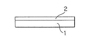
antenna, an Au film 2 with a thickness of approximately 100 nm is formed on
the major surface of a MgO(100) substrate 1 by the vacuum deposition method,
as shown in Figure 1A. Then, the substrate 1 is set within a focused ion beam
device (FIB) for irradiating a Ga+-ion beam accelerated at 30 KeV to positions
forming junctions, as shown in Figure 1B. The diameter of the irradiated ion
CA 02134008 1998-04-29
.~_
beam is 50 nm. In order to form Ga+-irradiated regions (implanted layers) 3 on
the MgO substrate 1, ion beam current is controlled in a range of 1 pA to 60 nA.Subsequently, as shown in Figure 1C, the Au film 2 is removed
from the overall surface of the substrate 1. As a method for removing the Au
film, various methods may be employed. However, the preferred method would
be Ar+-ion milling at 450 eV or a wet method with a solution of 2.6 wt% of Kl
and 0.65 wt% of I for lesser effect on the substrate.
Thereafter, as shown in Figure 1D, YBaCuO (hereinafter referred
to as "YBCO") film 4 is deposited by a pulse laser deposition in the thickness
of 300 nm over the entire surface of the substrate. The YBCO film 4 over the
irradiated region 3 becomes a modified region 5 which serves as a normal
conductor region.
Subsequently, as shown in Figure 2, the YBCO film 4 forms a
wiring pattern across the Ga+-irradiated region 3, the wiring pattern being of 5,um in width and 30 ~m in length. The 30-,um length of the wiring pattern servesas a non-linear response portion 4a (see Figure 3). One end of the non-linear
response portion 4a is connected to an oxide superconductor thin film feed line
wiring pattern (hereinafter simply referred to as "feed line wiring pattern") 4b,
and the other end is connected to a patch-type antenna 4c.
The detail of the non-linear response portion 4a of the wiring
pattern in the dimension of the 5 ~m in width and 30 ,um in length is shown in
Figure 2.
Figure 2 shows the plan view and sectional side elevation of the
non-linear response portion 4a in the case where six Ga+-ion beams with 50-nm
beam diameter are irradiated with respective intervals of 2 ,um therebetween.
Figure 3 shows an example of one unit of the preferred
embodiment of the array antenna fabricated through the foregoing process. In
Figure 3, the dimension of the patch-type antenna 4c is determined based upon
the dielectric constant of the substrate 1 and resonance frequency of the
substrate. In the shown embodiment, where MgO substrate 1 has a 0.5-mm
thickness and 9.7 is the dielectric constant, when the resonance frequency is
~. . .
~. Y'
CA 02134008 1998-04-29
_
23 GHz, the preferred dimension of the patch is 1.9 mm x 2.8 mm. At the
center of the patch-type antenna 4c, the impedance becomes substantially zero,
and at the center of the lower edge when the patch is in rectangular
configuration without cut-out, the impedance becomes several kn.
In the shown embodiment, the patch-type antenna 4c is also
formed of YBCO oxide superconductor film. A thin bias line 4d is provided at
the side opposite to the portion where the patch-type antenna 4c is connected
to the non-linear response portion 4a, the bias line 4d biasing a direct currentto the non-linear response portion. It should be noted that an Au thin film 2 isformed in a thickness of 3 IJm on the entire surface of the back side of the
substrate 1.
The impedance of the non-linear response portion 4 set forth
above with respect to the shown embodiment is in the order of near zero n to
several hundreds of n, and the impedance of the non-linear response portion
can be realized by appropriately setting the value of L.
Figure 4 shows an example of the array antenna in which four
units of patch-type antenna 4c are arranged. In order to establish external
connection with a normal 50n-system, the impedance at the portion D of the
feed line wiring pattern 4b is designed to be 50n. However, at the summing
junction B where two signals are supplied, the feed line wiring pattern is
branched to two patch-type antennae 4c. Therefore, in view of impedance
matching, the impedance of each of the two branches on the antenna side is set
at 100n, and on the other side (side near the portion D) is set at 50Q. In the
shown embodiment, the feed line wiring pattern providing the impedance of
100n has a width of approximately 80 ,um, and the feed line wiring pattern
providing the impedance of 50Q has a width of approximately 500 ~Jm.
The reason why the non-linear response portion 4a is provided at
the portion A will be discussed with reference to Figure 4. If the non-linear
response portion 4a were provided at the portion B, the high-frequency signal
received by the patch-type antenna 4c would have to pass through the high
impedance (100Q) feed line wiring pattern of approximately 80 ,um width from
CA 02134008 1998-04-29
i ,_
the portion A to the portion B. In such case, the high-frequency signal would
need to be transformed into a lower frequency signal at the portion A and then
transferred to the portion B to pass through the non-linear response portion.
This causes greater resistance loss than in the case where the non-linear
response portion is provided in the portion A. On the other hand, when the non-
linear response portion 4a is provided in the portion C or D, there would arise
a problem specific to the non-linear response portion, in addition to the problem
caused by the greater resistance loss at the higher frequency. The problem is
that the non-linear response efficiency can be lowered at relatively small high-frequency power. Specifically, in comparison with the portion A, approximately
twice as much power is concentrated at the portion C and four times as much
power is concentrated at the portion D. This means that the non-linear
response portion 4a becomes more sensitive to the power received at the patch-
type antenna for a higher power level at the portions C and D, and this possiblylowers the non-linear response efficiency for lower power level high-frequency
signals received by the patch-type antenna. In the shown embodiment, since
each of the non-linear response portions 4a is incorporated in each of the
corresponding patch-type antennae 4c, greater high-frequency power can be
received by the antenna.
On the other hand, as shown in Figure 4, direct current bias lines
4d are extracted out of the substrate from respective patch-type antennae 4c,
each of the direct current bias lines providing the direct current bias
independently of the other. With this construction, the transformation efficiency
and phase variation of the non-linear response portion 4a can be independently
controlled by the direct current bias. Therefore, a function such as a phase-
controlled antenna can be easily provided.
In order to bias the current for the non-linear response portion 4a
of Figures 3 and 4, current is supplied from the direct current bias line 4d andthe feed line 4b. A method for supplying a LO signal from the patch-type
antenna 4c or the feed line wiring pattern 4b is illustrated in Figure 5.
CA 02134008 1998-04-29
Figure 5 schematically shows a construction of one embodiment
of measuring equipment for evaluating the characteristics of a frequency-mixing
array antenna. In Figure 5, 23-GHz RF signal 11 and 22-GHz LO (local
oscillation) signal 12 are transmitted from a single horn antenna 13 and
irradiated on a frequency-mixing array antenna 15 placed within a refrigerator
14. A quartz window 16 is provided in the refrigeration 14 so that the RF signal11 and the LO signal 12 can be irradiated onto the frequency-mixing array
antenna 15 even when the antenna is placed inside the evacuated insulated
space. A difference frequency between the RF signal 11 and the LO signal,
called an intermediate frequency (IF), is 1 GHz in the shown case. Passing
through the feed line of the frequency-mixing array antenna 15, the IF signal 17is output to the outside of the refrigerator 14. In addition, in order to provide
direct current bias for the non-linear response portion of the frequency-mixing
antenna, a current terminal 18 is also provided.
Figure 6 shows an example, in which one patch-type antenna 4c
shown in Figure 3 is measured by the measuring equipment of Figure 5. The
distance between the horn antenna 13 and the frequency-mixing array antenna
was approximately 10 cm. The temperature of the superconductor non-linear
response portion 4a was approximately 33~ K. From the output of the horn
antenna, with an RF signal 11 of-40 dBm and a LO signal 12 at-30 dBm, an
IF signal output of -80 dBm was obtained. In Figure 6, the vertical axis
represents the IF signal output and the horizontal axis represents the bias
voltage applied to the non-linear response portion 4a. Even when at least -20
dBm of power was provided for RF signal 11 and LO signal 12, and with an
output power of the horn antenna of at least -20 dBm for both of the RF signal
11 and the LO signal 12, an increase in the IF signal was not observed.
As in the example set forth above, in general, the superconductor
non-linear response portion 4a has characteristics that cause lowering of
performance at a power at least equal to the RF power, and do not cause an
increase in the IF signal despite an increase in the RF signal. As a result, theprior art schemes which place the superconductor non-linear response portion
CA 02134008 1998-04-29
."
4a at the portion C or D of Figure 4, have lower performance than that of the
present invention in view of the range of RF power to be handled.
Placement of the non-linear response portion 4a at the portion A
(see Figure 4), in the vicinity of the patch-type antenna at the high-frequency
range, which cannot be achieved in the prior art, has been achieved by a novel
fabrication process according to the present invention.
Conventionally, the non-linear response portion 4a is formed by a
GaAs semiconductor element and requires functional connection of the
semiconductor element in a hybrid manner. Connection at precisions in the
order of a micron is not practical for the array antenna for high frequency
because it requires a high package density. Even in the monolithic structure,
in which the non-linear response portion is formed simultaneously with the feed
line, it has not been technically possible to package in the form of an array a
micron-size semiconductor non-linear response element operated at a frequency
of several tens of GHz. Therefore, in the prior art, at the portions C and D (see
Figure 4) or at further downstream portions where power is further concentrated,a lesser number of non-linear response portions are required in comparison with
the number of the patch-type antennae. Also, a relatively wide area for
installation can be provided.
As set forth above, according to the preferred embodiment of the
fabrication process of the array antenna as discussed with respect to the
process illustrated in Figures 1A to 1 D, the non-linear response portion 4a canbe provided at the portion A (Figure 4) in the vicinity of the patch-type antenna
4c. With the fabrication process according to the present invention six SNS
junctions can easily be formed within an area of 5 ,um x 30 ,um, for example.
In the fabrication process according to the present invention, by employing a
focused ion beam, the monolithic structure of the antenna and the feed line can
be formed with high precision, both in size and position, in a smaller area. This
definitely contributes to further increasing the package density.
With the array antenna according to the present invention, the
electromagnetic wave signal input from the antenna side is transformed into a
CA 02134008 1998-04-29
Iower frequency across the non-linear response portion, and the lowered
frequency of the electromagnetic wave signal is transferred through the oxide
superconductor film feed line wiring pattern. Therefore, the impedance
matching can be established between the antenna portion and the non-linear
response portion without requiring any special impedance circuit, permitting usein a substantially low loss range. Therefore, the superconductor antenna can
be used for a higher frequency electromagnetic wave.
Also, since respective individual elements of the array antenna
may suppress phase or amplitude of the signal, further delicate multi-functioning
can be achieved.
It should be noted that while MgO is employed as a crystalline
substrate in the embodiment set forth above, the material for forming the
substrate should not be limited to MgO, but could be SrTiO3, NdGaO3, LaAlO3,
LaGaO3 or a similar material, and also crystalline mixtures thereof. Also, whilethe YBCO film is formed on the substrate 1 to form the patch-type antenna and
the feed line on a common plane with the YBCO-film signal transmission line,
it should be evident that the antenna portion could be formed as a laminated
structure of the superconductor and a normal conductor, or solely as the normal
conductor.
If it is possible to reduce the high-frequency power of each
individual antenna by packaging the high density fine antenna at a higher
package density, it should be evident to those skilled in the art to place the non-
linear response portion at a slightly distanced position on the feed line, within
a range where the impedance matching can be established.
While the embodiment where the patch-type antenna and the feed
line are formed on the common plane has been discussed above, it is possible
that the major part of the array antenna can be constructed as illustrated in
Figure 7. The construction illustrated in Figure 7 is also an evident application
of the present invention for lowering the high-frequency power. The position of
the non-linear response portion 4a is determined in view of establishing
impedance matching between the patch-type antenna 4c and the non-linear
CA 02134008 1998-04-29
" __
response portion 4a. Specifically, in the construction of Figure 7, a second
pattern 21 consisting of a superconductor or a normal conductor covers a
portion of the patch-type antenna pattern 4c. The second pattern 21 is coupled
with the antenna pattern 4c in electromagnetic field coupling so that the second5 pattern 21 may serve as the antenna. Then, the antenna pattern 4c may serve
as a part of the feed line. Seeing that the non-linear response portion in the
layer below the second pattern 21 is a high-frequency response circuit, the
second pattern 21, the antenna pattern 4c is regarded as a part of the lower-
layer feed line. The second pattern 21 and the non-linear response portion 4a
10 form the structure according to the present invention. Specifically, the
construction shown in Figure 7 can be used as the structure, a pattern having
stronger electromagnetic field coupling being added to the structure of the
present invention.
As set forth above, according to the present invention, the
15 superconductor film wiring pattern is formed in a plane extending in common
with the major reference plane, and the non-linear response element is provided
in the wiring pattern such that the antenna pattern for discharging and absorbing
high-frequency electromagnetic field is connected to one end thereof and the
signal transmission path pattern is connected to the other end, forming one unit.
20 By connecting a plurality of units through a plurality of signal transmissionpatterns, the high-frequency electromagnetic wave signal input from the antenna
side can be transformed into a lower-frequency electromagnetic wave across
the non-linear response portion, so that a lower-frequency electromagnetic wave
is transferred through the oxide superconductor film feed line, allowing
25 impedance matching between the antenna portion and the non-linear response
portion to be established without requiring any special impedance circuit.
Therefore, the superconductor can be used in the frequency range where the
resistance loss in transmission therethrough is substantially small. With the
construction set forth above, the array antenna permits greater-power high-
30 frequency signals to be handled, allowing the superconductor antenna to beemployed for high-frequency electromagnetic waves.
CA 02134008 1998-04-29
Also, since the phase and amplitude of the signal can be controlled
by a respective choice of components of the array antenna, delicate multi-
functioning can be achieved.
Also, according to the fabrication process of the non-linear
response portion of the present invention, the antenna pattern and the current
introduction terminal pattern can be formed by depositing a protective layer on
the substrate in the region where the non-linear element or the non-linear
element group are to be formed, forming irradiated regions by irradiating a
focused ion beam on the substldte, removing the protective layer, depositing an
oxide superconductor on the substrate, forming the non-linear element by the
plurality of irradiated modified regions and the non-modified superconductor
regions on both sides of each modified region, one end of the element forming
a signal transmission line, a metal layer being formed on the oxide non-modifiedsuperconductor at the other end, the antenna pattern and the current
introduction terminal pattern being formed by patterning the metal layer.
Therefore, an array antenna which is formed by high density packaging of high
density fine antennae for reducing the high-frequency power of each individual
antenna, can be easily fabricated. Also, the fabrication process according to the
present invention further contributes to high density packaging.
Although the invention has been illustrated and described with
respect to exemplary embodiments thereof, it should be understood by those
skilled in the art that the foregoing and various other changes, omissions and
additions may be made therein and thereto, without departing from the spirit andscope of the present invention. Therefore, the present invention should not be
understood as limited to the specific embodiment set out above but as including
all possible embodiments which can be embodied within the encompassed
scope and equivalents thereof of the features set out in the appended claims.