Note: Descriptions are shown in the official language in which they were submitted.
wo 93/23246 2 1 ~ 3 ~ û Pcr/us93/04541
. :
THIN FILM METALLIZATION AND BRAZING OF ALUMINUM NITRIDE
~ .
CROSS REFERENCE TO RELATEr~ APPLICATI()NS
This application is a continuation-in-part of copending USSN 07/881,926 filed
May 12, 1992.
FIELD OF THE INVENTION
The present invention relates generally to metallization for aluminum nitride
ceramics having ~he properties of low thermal expansion and high thermal conductivity.
More particularly, this invention relates to a metallization structure formed on an
aluminum nitride substrate and a method of producing the metallization structure on ~e
aluminum nitride substrate.
BACKGRQUND OF THE INVENT'iON
Ceramic substrates are widely used as substrates for electronic circuits, and more
recently as substrates for hybrid integrated circuits. In manufacturing a hybrid integrated
circuit, it is necessary to mount an integrated circuit chip and other metal members such
as bonding wires on the ceramic substrate by brazing or soldering. However, these
members cannot be directly bonded to the ceramic substrate. It is therefore generally
practiced to first form an electroconductive metallized layer on the ceramic substra~e and
then bond the metal members to the metallized layer.
Because of its high thermal conductivity, excellent heat dissipation and electric
insulating properties, aluminum nitride (AIN) substrates have been used as substrates for
elect;onic packages such as hybrid integrated circuits. AIN is used in place of alumina
(A12O3) because of AlN's improved heat dissipation capabilities, and in place of beryllia
(13eO) because unlike AIN, BeO is toxic and, thus difficult to handle.
When an electronic substrate is used, the substrate is usually joined with a metal
layer, so that a conductive metallized structure is formed on the surface of the AIN
substrate. Conventionally for AIN, this metallized st~.~cture has been a layer of Cu~ Au
SIJBSTITUTE SHEET
2~3'~
W O 93/23246 PC~r/US93/04541 ~'~
or Ag-Pd formed by the direct bond copper (DBC) method or by the thick film method.
However, this method of metallizing AIN does not result in a well-adhered
metallized layer, particularly when the package is subsequently processed at high
temperatures. When a wire or semiconductor element is brazed onto the metallized layer
S at a high temperature, the adhesion s~rength between the metallized layer and the AIN
substrate is greatly lowered and the metalliæd layer along with the wire or semiconductor
element may eventually peel off of the AIN substrate. Because of the problems associated
with the DBC method, metallization of AIN substrates has been attempted in a number
of other ways.
U.S. Patent No. 3,716,759 discloses a bonding system for use with an aluminum
nitride body and a semiconductor crystal providing contact metallization by depositing in
a vacuum a thin layer of a refractory metal such as chromium, tungsten, or molybdenum
followed by a thin layer of nickel which is in turn followed by a thin layer of silver. A
conventional soft solder is then utilized capable of alloying with silver which bonds
directly to leads and heat sink as well as the contact metallization.
U.S. Patent No. 4,761,345 discloses an aluminum nitride substrate having a
metallized layer containing titanium nitride (TiN) and at least one selected from the group
Mo, W, Ta, an element of group lIIa, IIIb, and IVb of the periodic table, a rare earth
` element and an actinide element. The metallized layer is formed by dispersing the
powder of the respective elemen~s of the metallization composition in a binder to forrn
a paste, attaching the paste onto the surface of the AIN sintered substrate by dipping or
coating, followed by calcination by heating. The resulting metallized layer may
comprise, for example, W-TiN. A protective layer of nickel may then be electrolessly
plated or electrolytically plated onto the metallized layer.
U.S. Patent No. 4,770,953 discloses an aluminum nitride sintered body having
a metallized layer formed from simultaneously sintering a paste or liquid containing a
conductive element belonging to a first group and an element belonging to a second
group. The conductive element of the first group may be tungsten or molybdenum,
among others and the element of the second group may be titanium, hafnium, or
zirconium, among others. When titanium is the element of the second group, titanium
exists in the metallized layer as TiN.
U.S. Patent No. 4,873,151 discloses an aluminum nitride substrate having a
8UBSTITUTE SHEET
~ wo 93/23246 2 1 3 3 4 ~ Pcr~US93/04541
conductive material bonded to the AIN substrate through a metallized layer forrned on the
AIN substrate. The metallized layer contains at least one element selected fr~om Mo, W,
Ta and at least one element selected from the lIb, lIla, llIb and IVb group elements, and
rare earth elements. lt is not disclosed how this metallized layer is formed. The
- S conductive material which is bonded to the metallized layer has a thermal expansion
coefficient of between 2 x 10⁻⁶ to 6 x 1~6/C. This thermal expansion coefficient range
limits the usefulness of metallized AIN, since the typical conductive materials for
electronic circuits are Cu, Ag, Au and typical lead frame materials include Fe-Ni-Co
alloys. These materials have thermal expansion coefficients substantially higher than 6
X 10-6/C-
U.S. Patent No. 4,876,119 discloses a method of coating a nitride cerarnic
substrate by bringing a metal vapor into contact with the surface of the substrate. The
metal vapor reacts with an element present in the nitride ceramic substrate to form a
metallized layer on the substrate surface. For example, when Ti vapor is brought into
lS contact with the surface of an aluminum nitride substrate, it is disclosed that a layer of
TiN forms on the surface of the substrate.
U.S. Patent No. 4,980,239 discloses a metallization structure for AIN which
includes an intermediate layer of AlTiN formed on the AIN base, a Ti layer formed on
the interrnediate layer, a heat resistant metallic layer of W or Mo formed on the Ti layer
and a layer of Ni formed on the heat resistant metallic layer for soldering or brazing. It
is disclosed that the heat resistant metallic layer prevents inner dîffusion between Ti layer
and the Ni layer.
U.S. Patent No. 5,063,121 discloses a metallized AlN substrate having a
metallized layer formed by first coating a paste containing compounds of yttria and
alumina onto the substrate, followed by coating a metallized paste of Mo or W, TiO2 and
a binder onto the yttria and alumina coating. The coated substrate is then fired to form
a metallized layer of TiN and Mo or W on the AIN substrate.
Whereas there have been several methods proposed for metallizing AIN, few of
these mothods result in a ductile metallization structure having strong ceramic to metal
adhesion. Ductility is an important property because the metallization structure must be
able to withstand the stress caused by thermal cycling or mechanical vibration during
manufacture and operation of the electronic package. TiN, which is used in most
.
SUBSTITUTE SHEET
213 ~?~3
wo 93/23246 pcr/us93/o4s41
metallization methods, is a brittle compound and its presence in the metallization structure
lowers the fracture energy of the metal/ceramic interface and thus, c~an lead tocatastrophic failure when the metal/cerarnic interface is stressed.
Furtherrnore, the metal/ceramic interface must be resistant to embrittlement by
5 hydrogen. Hydrogen is used in the various operations of electronic packaging such as
brazing and annealing. In addition, hydrogen is a by-product of electrodeposition. A
metallization structure composed of Ti metal is not resistant to hydrogen embrittlement.
Thus, it is an object of the present invention to provide an adherent metallization
structure for aluminum nitride cerarnics. It is another object of the present invention to
10 provide a metallization structure for AIN ceramics that is resistant to embrittlement by
hydrogen. It is yet another object to provide a metallization structure that is sufficiently
ductile to withstand the stresses associated with electronic package manufacture and
operation.
SUMMARY OF T~E lNVENTlON
The present invention achieves a metallization structure for AIN ceramics that is
well adhered to the AIN ceramic, is resistant to embrittlement by hydrogen, and is
sufficiently ductile to withstand the stresses caused by electronic pa~kage manufacture and
operation.
An aluminum nitride metallized structure of the present invention includes a
~ ~ substrate comprising an AIN sintered body and a metallization strucnlre formed on the
;~ ~ substrate comprising a first layer deposited on the sintered body and a second layer
deposited on the first layer. The first layer comprises an alloy having the general formula
based on atomic percent
- XxZloo x
wherein X is at least one member selected from the group consisting of Ti, Zr, Hf, and
the rare earth elements, Z is at least one member selected from the group consisting of
Mo, W, Cr, Nb, V and Ta, and l0 < x <60 atomic %. The second layer comprises
at least one member selected from the group consisting of Au, Co, Cu, Ni, and Fe.
The present in~ention further includes an aluminum nitride substrate comprising
an AlN sintered body and a metallic alloy bonded to the substrate comprising at least one
member selected from the group consisting of Au, Co, Cu, Nit and Fe; at least one
8UE~STITUTE SHEET
W O 93/23246 2 13 ;~ 3 4 ~ PC~r/US93/04541
member selected from the group consisting of Ti, Zr, Hf, and the rare earth elements;
at least one member selected from the group consisting of Mo, W, Cr, Nb, V and Ta;
and less than about 1% of nitrides or aluminides of members selected from the group
consisting of Ti, Zr, Hf, and the rare earth elements; and having an elongation at room
5 tempera2ure greater than 5 % .
The present invention also includes an aluminum nitride substrate having a lead
frame bonded thereto by a metallic alloy structure, wherein said metallic alloy struc2ure
comprises
i) greater than 80 weight percent silver and copper,
ii) less than 2 weight percent of an element selected from at least one of Ti, Zr, Hf and the rare earth elements,
iii) at leæt one element selected from Mo, W, Cr, Nb, V, and Ta. ;
The metallic alloy structure may further comprise at least one element selected
from Au, Co, Ni, and Fe.
BRIEF DESCRIPTION OF THE DRAWINGS
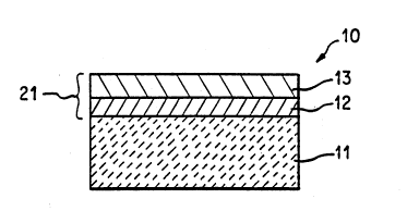
FIG. 1 is a cross-sectional view of the aluminum nitride metallized structure ofthe present invendon before brazing.
FIG. 2 is a cross-sec2ional view of the aluminum nitride metallized structure of20 the present invention including an additional ductile layer before brazing.
FIG. 3 is a cross-sectional view of the aluminum nitride metallized structure ofthe present invention after brazing and including an attached lead frame.
PIG. 4 is a cross-sectional view of a further embodiment of the aluminum nitridemetallized structure of the present invention after brazing and including an attached lead
25 frame.
DETAlLED DESCRIPTlON OF THE lNVENTlON
A description of the preferred embodiment of the present invention is given withreferencè to Pigures 1-3. Referring to Pigure l, the preferred embodiment of the present
30 invention comprises an aluminum nitride ceramic substrate 11, a first thin film layer 12
formed on AlN substrate 11, and a second ~in film layer 13 formed on first thin film
layer 12.
8UBSTITUTE SH~ET
wo 93~232~ L ~ Pcr/us93/o454l
AIN ceramic substrate 11 may be produced by a conventional process comprising
the steps of forming an AIN powder to obtain a body having a desired shape, and then
sintering the formed AlN body. Sintered AIN substrates are comrnercially available, for
example from The Carborundum Company, Niagara Falls, New York.
S Before first thin film layer 12 is formed, the surface of AIN substrate 11 is
cleaned by washing in a solvent such as ethanol or methanol followed by air drying.
First thin film layer 12 has a thickness preferably in the range 100-5000A, and more
preferably in the range 2sO-1500A. The temperature of the AIN ceramic substrate 11
during the deposition of first thin film layer 12 is set within the range of about 25~00C.
First thin film layer 12 is forrned on AIN ceramic substrate 11 by a chemical orphysical vapor deposition such as sputtering or vacuum evaporation. First thin film layer
12 comprises an alloy having the general formula based on atomic percent XXZloo-x~
wherein X is at least one metal selected from the group consisting of Ti, Zr, Hf, the rare
earth elements; Z is at least one metal selected from the group consisting of Mo, W, Cr,
Nb, V, Ta; and 10< x <60. If the first thin film layer 12 comprises Hf or Zr as the
X component in the formula XxZloo-x~ then preferably 10 ~ x ~ 30 atomic %.
Next, as shown in Figure 1, a second thin film layer 13 is formed on top of the
first thin film layer 12 by a conventional process such as sputtering. Second thin film
layer 13 is composed of at least one metal selected from the group consisting of Au, Co,
Cu, Ni, and Fe and is about 1-10 microns thick. Preferably, second thin film layer 13
comprises an alloy of Ni and Cu. More preferably, second thin film layer 13 comprises
an alloy of Ni and Cu wherein the Cu content is in the range of about 40-90 atomic %.
Second thin film layer 13 permits the fastening of a member such as a metallic member
to metallized structure 10 by soldering or brazing.
2S Following the deposition of first and second thin film layers 12 and 13, sharp
interfaces are obser~ed between the metallic layers and AIN ceramic substrate 11. There
is also observed a sharp interface between first thin film layer 12 and second thin film
layer 13. Thus, no reaction or mixing between the thin film metallic layers or between
the first thm film metallic layer and the AIN ceramic substrate have been observed prior
to heat treatrnent.
The present invention will be described in detail by way of its examples.
SUBSTITUTE SHEET
W0 93/23~46 ~ 1 3 ~ 3 1 0 PCr/US93104541
EXAMPLE 1
A sintered AlN substrate measuring 2" x 2" and having a thickness of 25 mils wasultrasonically cleaned in ethanol and dried in air at about 350C~ A thin film layer of
Ti2gW71 was deposited on the substrate by DC magnetron sputtering. The deposition
S was carried out in a cryopumped (base pressure of S x 10-8 torr) chamber using Ar
sputter gas (pressure of 3 microns). The rate of deposition was 300 A/min and the
temperature within the chamber was in the range 50-100C. The thickness of the
resulting Ti2gW71 thin film layer was about 0.5 microns.
After the first thin film layer of Ti2gW71 was deposited, a thin film layer of Ni
10 was deposited by magnetron sputtering. The thickness of the Ni layer was a~out 1.0
microns.
EXAMPLES 2-9 and COMPARATIVE EXAMPLES a-f
; ~ 15 The metallized structures of Examples 2-9 and Comparative Examples a-f were
prepared substantially in accordance with Example 1, except the composition of the first
thin film layer was varied. A second thin film layer of Ni having a thickness of about
1.0 ~Im was deposited on the first thin film layer by magnetron sputtering. Table I shows
the composition of Examples 2-9 and Comparative Examples a-f.
The adhesive strength of the metallization structure 21, which is comprised of first
thin film layer 12 and second thin film layer 13, was measured in a peel test. The test
consists of soldering a wire to second tbin film layer 13, bending the wire to a 90 angle,
and then pulling the wire in the direction perpendicular to the plane of the substrate.
The adhesive strength was measured and compared for various samples of the
structure of the present invention before and after exposure to hydrogen gas at 100C for
24 hours. This exposure to hydrogen gas simulates one of the failure modes tbat can
occur during the processing of an AIN substrate. For example, operations such asbrazing are conducted in a hydrogen-containing atmosphere at elevated temperature. In
addition, bydrogen can be generated during the electrodeposition of metals such as Ni and
Cu. Table I demonstrates the results of the peel test for Examples 1-9 as well as for
Comparative Examples a-f.
SUBSTITUTE SHEET
wo 93~23246 Pcr/uss3/o4s4~
2 1 3 ~
TABLE I
Composition Adhesion before Adhesion a~er
of first thin hydrogen exposure hydrogen exposure
ExamPle film laver (Ibs) Ll~
1 W -29Ti > 12.0 > 12.0
2 W -40Ti > 12.0 > 12~0
3 W -48Ti > 12~0 > 12~0
4 M o-30Ti > 12.0 > 12.0
Cr-40Ti > 14.0 > 13.0
6 W-20Y > 12.0 not tested
7 W-32Zr > 14.0 > 14.0
8 Ta-25Y > 13.0 not tested
9 Cr-lOMo-25Zr > 12.0 > 12.0
Comparative
Example
- a Cr 5.6 4.8
b Mo 2.0 2.5
c W 3 5 3 5
- 25 d Ti > 12.0 0.0
e W-9at%Ti 4.0 3.5
f W-80at%Ti > 13.0 7.5
We have observed that when the first thin film layer comprises Ti-W alloys
having between 10 and 60 atomic % Ti, the peel test values remain greater than 12 Ibs
force after exposure to hydrogen. The drop in adhesive strength observed when the
Ti content exceeds 60 atomic % (examples d and f), may be the result of hydrogenembrittlement of the resulting Ti-W alloy.
Ihe elemental films of Cr, Mo and W exhibited poor adhesion to the AlN
substrates as demonstrated by Table I, Examples a-c. This poor adhesion may be the
result of poor chemical bonding of these metals to the AlN substrate. It is alsopossible that impurities from ~he AIN substrate surface, for example oxygen, carbon,
or water, are incorporated into the growing film at the metal/AlN interface, thereby
rendering it brittle and poorly adhered to the AlN substrate.
It is possible to obtain a patterned metallization layer on the AlN ceramic base11. For example, after the thin film layer 12 and thin film layer 13 have been forrned
on the AlN ceramic base 11, AlN metallized structure 10 is subjected to a
8UBSTITUTE SH~ET
.~ W O 93/23246 213 Ll 3 I ~ PC~r/US93/04541
conventional patterning process in which an etchant liquid containing a mixed acid of
hydrofluoric acid and nitric acid is used.
After deposition of first thin film layer 12, it is preferable that thin film layer
12 have a substantially body-centered-cubic crystal structure. For many of the alloys
S described above, this is a non-equilibrium structure. However, it is the most ductile
and compliant form of the subject alloys, and therefore, the most desirable for the
purpose of the present invention. Brittle intermetallic compounds such as Cr2Ti and
Cr2Ta are preferably avoided. In applications in which the metallized structure will
be exposed to temperatures above 500C, such as in brazing, it is important that the
dùctility of first thin film layer 12 persist after exposure to high temperatures.
The second thin film layer 13 is preferably ductile, in addition to being
relatively &ee of embrittling agents such as oxygen and carbon. As shown in Figure
2, an additional optional layer, ductile layer 14, is deposited on the thin film layer 13
before brazing. Ductile layer 14 is selected from the group consisting of Ni, Co, Cu,
Au and alloys thereof. Preferably, ductile layer 14 comprises electrolytically
deposited Ni.
During brazing, first thin film layer 12 reacts with second thin film layer 13 to
form metallic alloy structure 15, as shown in Figure 3. Metallic alloy structure 15
- comprises an alloy of the metals of the first and second thin film layers 12 and 13 and
ductile layer 14, if any. To insure that metallic alloy structure 15 possesses sufficient
ductili~ for reliable perforrnance, an excess of the metal comprising second ~in film
;~ / layer 13 may be added to the metallic structure via the addition of ductile layer 14
before brazing. For reliabb performance, metallic structure 15 should preferablyhave greater than 5% elongation at break, and more preferably greater tnan 15%
elongation at room temperature. To achieve this, the thickness of tnin film layer 13
and ductile layer 14 combined should be at least S times greater tnan the thickness of
~in film layer 12. ln other words, greater than about 80 atomic % of the metallic
alloy comprises at least one member of the group consisting of Ni, Cu, Co, Fe and
Au.
If the composition of second thin film layer 13 and the braze composition form
a metallic alloy under ~e braze conditions used, then after the brazing operation layer
15 will contain tne elements of thin film layers 12 and 13 (and optionally ductile layer
8UBSTITU~E SHEET
wo 93~23246 PCr/USs3/0454l ~ - ~
2 1 3`~
14) as well as the elements in the braze.
For example, in the metallization system of the present invention, if ~second
thin film layer 13 is a nickel-copper alloy having greater than 10 weight percent
copper, and the braze used is a silver-copper braze having more than 50 weight
5 percent silver and a thickness of greater than or equal to about 25 microns, then after
brazing, layer 15 will be a metallic alloy structure bonded to the substrate comprising
i) greater than 80 weight percent silver and copper;
ii) less than 2 weight percent of an element selected from Ti, Zr, Hf, and the
rare earth elements,
iii) less than 2 weight percent of an element selected from the group consistingof Mo, W, Cr, Nb, V, and Ta;
iv) less than 20 weight percent Ni;
v) less than 1 weight percent (if any) of nitrides or aluminides of Ti, Zr, Hf or
- the rare earth elements and having an elongation at room temperature greater
than 5%.
Alternatively, the second thin film layer before braze may comprise at least
one element selected from Au, Co, Cu, Fe and Ni, and these elements may then
appear after braze in met~llic alloy structure 15.
The adhesive strength of metallic alloy structure 15, the structure formed after20 brazing, was measured according to the peel test described above. Table II
demonstrates the results of the peel test for different embodiments of the present
invention as well as for comparative examples.
SUBSTITUTE SHEET
2~3~i3~3
;~ WO 93~2324~ PCr/USs3/0454l
TABLE Il
Composition of Composition of Adhesion after
S ExamPle first laver second laver brazinE Lbs)
W-29at%Ti Ni > 12.0
11 W-40at%Ti Ni > 14.0
12 W-40at%Ti Ni-SOat%Cu ~ 18.0
13 W-50at%Ti Cu ~ 16.0
14 Mo-30at%Ti Ni > 12.0
Cr-40at%Ti Ni-70at%Cu ~ 21.0
15 Comparative
Example
g W Ni Cl.O
h Mo Ni < 1.0
i Cr Ni < 1.0
W-lOat%Ti Ni 4.8
Examples 10-15 and Comparative Examples gj were prepared substantially in
accordance with example 1, except that the thickness of the second thin film layer was
2.5 microns. In addition, the second thin film layers of exarnples 12, 13 and 15comprise copper.
The metallized substrates of examples 10-15 and gj were brazed to copper
pads for adhesion testing. The metallized substrates were mounted in a furnace with
25 microns thick Ag-27Cu(wt%) braze preforms placed on the metallized substrates,
followed by lmm thick copper pads placed on the metallized substrates. Brazing was
carried out in an Ar or H2 atmosphere at 825C for 5 minutes, followed by cooling to
room temperature over a period of about 20 minutes. Other suitable brazes include
Ag, Ni, Cu and Au based brazes, such as, for exarnple, Au-20Ge, Ni-SB,
Ag-25Cu-5Sn and Ag-SAI.
The elemental films of Cr, Mo and W of Comparative Examples g-i, exhibit
unacceptably poor adhesion following brazing. Excellent adhesion after brazing was
observed for the materials of the present invention, Examples 10-15. The strength of
the metallAlN interface is measured by the fracture energy of the metal/AlN bond.
The failure mechanism for Examples 10-15 following testing was fracture of the AIN
ceramic near the metal/AlN interface. This indicates that the interfacial metal/AlN
SUBSTITUTE SHEET
WO 93/23246 Pcr/uS93/04541 ~ ~
2 1 3 '~
bond is actually stronger than the AIN cerarnic and thus, represents the maximumuseful strength for a metal/AlN bond. This superior bond strength is most evident for
compositions in which the value for x representing the content of X in the formula
XXZ100-X in the first thin film layer is greater than about 30 atomic %.
S Following the brazing and testing of the examples of Table Il, a number of the
examples were microstructurally analyzed using Scanning Auger Microprobe. This
testing included both a polished cross-section of the brazed parts as well as depth
profiles from the metallized su!face down to the AlN surface. In Examples 10-lS, a
similar microstructure was observed. The first and second layers were found to have
extensively reacted to form a metallic alloy rich in the second layer components. ;
Interstitial atoms such as oxygen and carbon have been reduced to low levels at the
interface and more significantly, have preferentially reacted with the X component of
the XxZloo-x first layer alloy to form dispersed oxides or carbides. `
Near the interface, X-ray Photoelectron Spectroscopy indicates the presence of
both metallic and partially oxidized X component elements, while the other
components are in fully metallic states. This insures the ductility of the resulting
metallic ~hase in the metallization. No brittle compounds were observed and
substantially no reaction of the metallization components and the AIN ceramic could
be detected. I ess than about one percent of the metallic alloy consisted of nitrides or
aluminides of the X compound of tne first layer alloy, the products of potential- reactions of the metallization components and AlN. This structure, established by the
; choice of the first and second layer compositions and their relative thicknesses,
determines the excellent performance of these materials.
The desired microstructure of the metallic alloy near the AlN interface
following brazing or other high temperature exposures greater than S00C, based on
the present invention, is one in which the bulk of the metallic alloy consists of metallic
phases of the components of the first and second layers in which less than 10 percent
by volume is intermetallic compounds, such as Cr2Ti or NiTi, and at least 25% of the
starting amount of the X component of the first layer alloy is in the metallic state as
determined by X-ray Photoelectron Spectroscopy. Further, less than about one
percent by volume of the metallic alloy consists of brittle compounds such as TiN and
Ni-AI-oxides, and less than 2.5 atomic % oxygèn is left in solid solution in the
SUBSTITUTE SHEET
WO 93/23246 2 1 3 ~ ~ 4 ~ PCr/US93/04541
1, ,~ ' ' '
metallic alloy. In addition, the majority of the embrittling agents such as oxygen,
carbon, and nitrogen are associated with the X component of the first layer alloy in
the form of discontinuous, dispersed particles in the metallic alloy. The resultant
- metallization has an elongation at room temperature greater than 5 % and preferably
- S greater than 15% at break.
To examine a brazed, metallized AIN substrate, a sintered AIN substrate was
sputtered with a two-tenths (2/10) micron thin film layer of 20 wt% titanium and 80
wt% tungsten, followed by the deposition of a separate two (2) micron layer of 60
wt% copper and 40 wt% nickel.
The substrate was not intentionally heated during sputtering, and the maximum
temperature experienced by the structure was about 200C due to the energy of the
deposition. There was no reaction detected during the sputtering process between Ti
or W and the components of the substrate, or bet~,veen the Cu or Ni and the Ti or W.
A copper clad -lead frarne was brazed onto the metallized substrate with a 25
micron thick braze composition of Ag - 27 wt% Cu at between 780-900C. The
resuldng metallic alloy structure had an average composition by weight % of Ag 66 -
Cu 29 - Ni4 - TiO.03 - WO.1.
The metallic alloy structure 41 had three compositional zones, as depicted in
Fig. 4. ln aluminum nitride substrate 40, zone 22 contiguous to substrate 21 and zone
23 contiguous to lead frame 25 were copper-rich, and zone 24 was silver-rich. The
copper cladding was consumed in the brazing process, providing more volume to the
braze.
The foregoing exarnples are not intended to limit the subject invention, the
breadth of which is defined by the specification and the claims appended hereto, but
are presented rather to aid those skilled in the art to clearly understand the invention
defined herein.
SUBSTITUTE SHEET