Note: Descriptions are shown in the official language in which they were submitted.
- ~134672
WO 93/22796 PCI/~lS93/03790
"MOS (iATED THYRISTOR WITH REMOTE TURN-OFF ELECTRODE"
The present invsntion relates generaliy to th~ field of four-layer, latching
semiconductor devices, and particularly to methods for controlling the conduction
characteristics of such devices by modulating tha voltage applied to the gate
electrode of a MOS field effect transistor (MOSFET) portion of the device.
BACKGROUND OF THE INVENTION
The development of power MOSFET's was at least in part motivated by the
objective of reducing the control current required by power bipolar devices during
10 forced turn-off. In bipolar devices the injection of minority carriers into their drift
region reduces the resistance to forward current flow. These devices are capableof operation at appreciable current densities, but are relatively inefficient as a
consequence of the large currents required during device turn-on and turn-off.
15 In contrast, the gate structure of the power MOSFET has a very high steady-state
impedance. This allows control of the device by a voltage source, since only
relatively small gate drive currents are required to charge and discharge the input
gate capacitance. Unfortunately, the ease of gating the power MOSFET is offset
by its high on-state resistance arising from the absence of minority carrier
20 injection. Hence, a combination of low-resistance bipolar-type current conduction
with MOS gate control would provide the desired features of high operating
forward current density and low gate drive power.
213467~
WO 93/22796 PCT/US93/03790
Referring to the cross-sectional illustration of Fig. 1, a device known as an
insulated gate bipolar transistor (IGBT) illustrates one approach to combining
these features. In this type of structure most of the forward current flow occurs
between the emitter and collectorterrninals of the vertical PNP bipolartransistor
5 portion of the device. The on-state losses of the IGBT at high voltages are
significantly less than those of power MOSFET's due to the injection of minoritycarriers (electrons) into the N-base drift region.
. As shown in Fig. 2, a regenerative device known as MOS-controlled thyristor
10 (MCT) exhibits less forward voltage drop than does the IGBT. This P-N-P-N
structure can be regarded as two transistors - an upper NPN transistor and a
lower PNP transistor - that are intemally connected in such a fashion as to obtain
regenerative feedback between each other. Specifically, a thyristor may be
considered as a combination of PNP and NPN bipolar transistors connected such
15 that the base of each is driven by the collector current of the other. Once the
thyristor is tumed on via the gate electrode such that the requisite transistor
~; ~ turn-on current is supplied each transistor then drives the other into saturation.
At this juncture the thyristor is no longer under the control of its gate electrode
and continues to operate even in the absence of gate drive current. This
20 phenomenon is known as regenerative latch up.
Since thyristors are often used in high-power switching applications, the maximum
tum-off current level is generally of considerable importance. The MCT device
of Fig. 2 is tumed off by reversing the polarity of the applied gate voltage so as
25 to eliminate the accumulation layer at the surface of the N-region embedded
between the P and P+ regions underlying th0 gate. In this way a p-channel
field-effect transistor (FET) within the device forms an active short circuit between
the N+ cathode and P-base regions~ The device will cease regenerative operation
when the short-circuit current increases to the extent that the voltage across the
30 N+/P junction falls below 0.7V. Unfortunately, the maximum current which can
be switched off by the MCT markedly decreases with increasing anode voltages
at elevated temperatures. As a consequence, the current handling capability
of the MCT has proven to be inadequate for particular circuit applications.
2134~72
WO 93/22796 . PCr/US93/03790
Fig. 3 depicts a four-layer semiconductor structure, generally tenned a MOS gated
emitter switched thyristor (EST~, also designed to operate in a regenerative mode.
When the gate voltage is at the cathode potential the device is in a forward
blocking mode with the anode voltage supported across junction J 1 . The device
5 is tumed on by applying a positive bias to the gate to ~reate a channel at thesurface of the P-base region. As shown in Fig. 3, the regenerative thyris~or
portion of the device latches upon fo~ward bias of the junction between an N+
floating emitter and a P-base included within a lateral MOSFET struc~ure at the
surface of the device. Regenerative operation is extinguished by reducing the
10 gate bias to zero, effectively disconnecting the emitter from the cathode~
However, the N I /P junction of the thyristor does not become reverse biased until
the regenerative action of the main thyristor is sufficiently attenuated. It follows
that the lateral MOSFET at the surface of the structure is prone to break down
during high-voltage device deactivation as a consequence of supporting the large- 15 junction voltage. Moreover, the elevated hole current through the cathode which
arises during tum-off of the device may induce undesired regenerative operation
within a parasitic thyristor (Fig. 3).
Accordingly, a need in the art exists for an emitter switched thyristor disposed20 to be turned off rapidly (i.e., less than 1 microsecond) without accompanyingparasitic thyristor latch up.
SUMMARY OF THE INVENTION
25 The present invention addresses the foregoing objectives by providing an
improved emitter switched thyristor structure having a remote turn-off electrodedesigned to improve maximum current turn-off capability and reduce device
turn-off time. The improved thyristor structure includes anode and cathode
electrodes, with the remote electrode being connected to the cathode electrode.
30 A multi-layer body of semiconductor material has a first surface and includesregenerative and non-regenerative portions each operatively coupled between
the anode and cathode electrodes. The regenerative portion includes adjacent
first, second, third and fourth regions of alternating conductivity type arranged
2134572
W O 93/22796 PC~r/US93/03790
- 4 -
respectively in series. Electrical contact is made between the remote electrode
and the second region, as well as between the anode electrode and the fourth
region.
5 The inventive thyristor is tumed on by applying an enabling voltage to an
insulated gate electrode disposed adjacent the first surface such that a conductive
channel is created in the regenerative portion via modulation of the conductivity
therein. Sirnilarly, the termination of regenerative operation is initiated by applying
a non-enabling voltage to the gate electrode. The remote electrode collects any
10 charges remaining in the second region of the regenerative portion subsequentto application of the non-enabling voltage and thereby expedites turn off of th
inventive thyristor.
BRIEF DESCRIPTION OF THE DRAWINGS
Additional objects and features of the invention will be more readily apparent
from the following detailed description and appended claims when taken in
conjunction with the drawings, in which:
20 Figure 1 is a cross-sectional illustration of a conventional insulated gate bipolar
transistor (IGBT) device~
FigurP 2 shows a prior art P-N-P-N regenerative semiconductor device generally
known as a MOS-controlled thyristor (MCT)~
Figure 3 depicts a conventional implementation of a four-layer MOS gated emitterswitched thyristor (EST) semiconductor device.
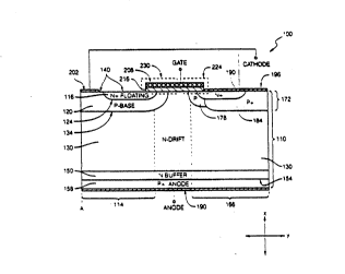
Figure 4 shows a cross-sectional representation of a preferred embodiment of
30 the inventive emitter switched semiconductor thyristor device with remote
electrode.
2134672
WO 93/227g6 PCl`/US93/03790
DESCRIPTION OF THE PREFERRED EMB~DIMENT
Referring to Figure 4, there is shown a cross-sectional representation of a
preferred embodiment of the improved ernitter switched semiconductor thyristor
6 device 100 of the present invention. In order to simplify explanation only one^half
of the inventive thyristor 100 is depicted in Fig. 4. The remaining one-half of
the thyristor 100 comprises a mirror image, with respect to an axis A, of the
one-half portion shown in Fig. 4. The thyristor 100 includes a body of
semiconductor material 110 having a four layer or regenerative portion 114
10 constituted by a floating emitter region 116 of N+ conductivity material, and by
a base region 120 of P conductivity material forrning a first PN junction 124 with
the floating emitter 116. A third layer of the regenerative portion of the thyristor
device 100 is identified as a drift region 130 consisting of N- semiconductor
material adjacent to and forming a second PN junction 134 with the base region
120. As shown in Fig. 4, the semiconductor body 110 is bounded by a
substantially planar upper surface 140 defined in part by the uppermost portionsof the floating emitter 116, base 1 2û and drift 130 regions. A set of referencerectangular coordinates are included in Fig. 4 and are used in the following
description to specify direction.
The drift region 130 includes an optional N-type buffer region 150, and separates
the base 120 from a fourth layer, or P+ anode region 158, of the regenerative
portion of the thyristor 100. Adjacent to the four layer, regenerative portion 1 14
is a three layer, non-regenerative structure 166 comprised of a tri-component
cathode region 172, the drift region 130, and the anode region 158. The cathode
region 172 includes a well structùre consisting of diffusions of P and P+ material
178 and 184, with an N+ diffusion 190 disposed within the well defined by
diffusions 178 and 184.
Ohmic contacts exist between the lower surface of anode layer 158 and an anode
electrode 190, as well as between the upper surface 140 of the P+ and N+
diffusions 184 and 190 and a cathode electrode 196. In addition, the base region120 is in ohmic contact with a remote electrode 202 electrically coupled to the
~134672 PCT/US 93~03~90
6 lPE~/US 09NoV t9~3
ca~ode e ectrode 196. Each region of the reg~nerative 114 and non-regenerat~ve
portions 166 of ths improved thyristor 100 forms an elongated segment
perpendicular to the plane of Fig. 4.
P~eterring to Fig. 4, an insulated gate electrode 208 overlaps the upper surface140 of the regenerative 1 14 and non-regenerative 166 regions. Specifically, an
oxide layer 216 separates the ~lectrode 208 from the N+ d ffusion 190, P diffusion
178 and drift region 1 3û so as to form a first N-channel enhancement mode MOS
transistor 224. Similarly, a second N~hannel enharK ement mode MOS transistor
230 is created in series with the first ~ransistor 224 by the portions of the floating
emitter 116, base 120 and drift regions underlying the gate electrode 208.
With tha cathode and gate electrodes 196 and.208 held at the same potential
the thyristor 100 is in a forward blocking mode. In the blooking mode any voltage
differ~ntial between the anode and cathode electrodss 192 and 196 is pnmarily
supported by the PN junction 134. The device may be tumed on by applying
a positive bias to the gate electrode 208 of sufficient magnitude to create
inYersion layers at the surface of the base regions 17B and 120 of the first andsecond MOStransistors 224 and 230. Although conductive channels are fonned
in both transistors 224 and 230 upon application of the re~uisite gate voltage,
current initially flows exclusively through the first MOS transistor 224 due to the
floating drain (iOe~ the N+ emitter 116) of the second MOS transistor 230. At
these low current levels the thyristor device 100 operates similarly to the
conventional IGBT (Insulated Gate Bipolar Transis~or) shown in Fig. 1. In 1~3BT
mode operation the current flow through the regenerative portion 114 of the
device 100 has not yet become self-sustaining, and hence the anode current
remains dependent on the ma~nitude of the applied gate voltage.
Upon formation of the inversion layer in the first MOS transistor 224, electronst~ow trom the N+ region 190 into the driR region 13~ wher~ ~ serve as base
current for the PNP transistor inherent within the four !ayer regenerative portion
1 14. When a sufficient voitage is applied to the anode electrode 192 the resulting
current flow is adequate to induce regenerative thyristor action (i.e. Iatch up) SUBSTITUTE SHEET
IPEA~JS
~134672 P(T~US 93J03~90
7 IPEA/US O9NO\I
within the four layer portion 1 14. Subsequent to the initiation of such action the
anode current flow in th~ regenerative portion flows through both the first and
second MOS transistors 224 and 230. Tha anode current may therefore be
controlled by modulation of the applied gate voltage even after regenerative
5 thyristor action takes placs.
The onset of regenerative action (on-state) is precipitated by the flow of hole
currant to the remote electrode 202 through the segment of the base region 120
underlying the floating emitter 116. The sheet resistivity of the basa 120 and
10 length of the emitter 116 in the Y direction are selected to be such that the hole
current develops the potential (~0.7 Volts) requîred to forward bias the PN
junction 124. Specifically, the floating smittar 116 will typically span -~
approximately 20 microns in the Y direction while the shest resistivity of the base
120 is generally 3000 ohms per square. The dri~t region 130 is dimensioned
to ex~end approximately 50 microns ~rom the N-type buffer region 150 to the PN
junction 134, and is doped at 101 4/cm3. The carrier lif~times within the drift region
130 are on the order of 1 microsecond, with the tum off time of the device 100
being affecled thereby. ~he drift region doping level and thickness will generally
be chosen to meet sp~ified breakdown voltage requircments.
During operation in the on-state a substantial pe~centage of the anode current
flows vettically through the regenerative portion ~14, since it is in this region
where the fonvard bias across PN junction 124 allows a large number of electronsto be injected into the drift region 130 from tha floating emitter 116 of MOS
transistor 230. Nonetheless, the PNP transistor comprising the diffusion 184,
dri~t region 130 and anode layer 158 present within the non-regenerative portion166 a.so contributas to the on-state current flow. At vely high anode current
densities (e.g. 1000 A/cm2) it is possible that a parasitic thyristor comprising the
combination of the PNP transistor described above and the N+ dfflusion 190
will .atch up. As is explained more fully below, ~ is a feature of the present
invention that the hole collection capability aHorded by the remote electrode 202
reduces ~he likelihood of parasitic latch up during tum~oH by reducing the current
density proximate the PN junction between the diffusions 184 and 190.
SU~Ti.~ UTE SHE~T
IPE~VS
W O 9312279S 2 1 3 4 6 7 2 PC~r/US93~03790
When it desired to terminate regenerative operation the voltage impressed on
the gate electrode 208 is reduced to zero. The surfaces of the P-type regions
178 and 120 will preferably be sufficiently narrow (e.g. 1 to 3 microns in the Ydirection) that reduction in the gate voltage to zero will rapidly extinguish the
5 conductive channels within the first and second MOS transistors. This
disconnects the floating N I emitter region 116 from the cathode electrode 196,
thereby causing termination of regenerative thyristor action.
As mentioned in the Background of the Invention, the lateral MOSFET within
10 a conventional EST device (Fig. 3) is prone to break down when tum-off occursat high anode voltages because of temporarily being required to support such
voltages prior to termination of the regenerative action of the thyristor. The
present invention addresses this shortcoming of prior art EST devices by provision
of the remote electrode 202 to expedite charge removal from the base 120 upon
15 reduction in the potential applied to the gate electrode 208. As shown in Fig.
3, the only manner in which holes can be drawn from the base region of the
conventional EST device is through the cathode terminal. It follows that holes
present in the regenerative portion of the device proximate the floating emitiermust traverse the entire P-base region as well as the P+ diffusion in order to
20 be collected, thus increasing the probability of latch up of the parasitic thyristor.
Consequently, prior art EST devices are not generally capable of ceasing
regenerative operation at high current densities. In contrast, a remote-electrode
thyristor device fabricated in accordance with the present invention can operateat current densities above 1000 A/cm2.
As may be appreciated by referring to Fig. 3, the structure of conventional EST
devices results in a predisposition for latch up of the parasitic thyristor during
turn-off. Specifically, reducing the applied gate voltage in order to initiate
deactivation of the device induces a loss of channel conductivity between the
30 N~ cathode diffusion and the floating emitter, thereby decoupling the floating
emitter from the cathode. The fo~ard bias across the PN junction between the
P-base and floating emitter then diminishes as regenerative activity subsides,
and an excess hole concentration develops proximate the floating emitter as fewer
- 2134672
WO 93/22796 PCI /l)S93/03790
,9 .
electrons are injected thereT into the base. The requirement of charge ;
neutrality forces these holes ~o the cathode via the P+ diffusion, thus resulting
in a spike of hole current proximats the PN junction between the diffusions
underlying the cathode. If of sufficient magnitude, the current spike may forward
5 bias this PN junction and precipitate parasitic latch up.
Referring to Fig. 4, the remote electrode 202 serves to reduce any excess hole
concentration developing in the bsse 120 during tum off of the inventive thyristor
device 100. Specifically, holes prssent within the regenerative pclt.on 114 of
10 the device at the time of tum off will migrate along a low-impedance path to the
remote electrode 202 rather than through the regions 178 and 18~l to the cathodeelectrode 196~ This eliminates the flow of excess holes from the base 120
through the cathode region 172, and hence minimizes the likelihood of undesired
latch up of the parasitic thyriston ;~
While the present invention has been described with reference to a few specific
embodiments, the description is illustrative of the invention and is not to be
construed as limiting the invention~ Various modifications may occur to those
skilled in the art without departing from the true spirit and scope of the invention :
20 as defined by the appended claims~ Specifically, the thyristor devices
incorporating the teachings of the present invention may be embodied in
semiconductor structures which differ from that depicted in Figure 4~ For
example, the gate electrode may be bifurcated so as to independently control
the forrnation of conductive channels within the regenerative and non-regenerative
25 regions~ In addition, the cathode region need not be realized using the specific
arrangement of diffusions specified herein~ Those skilled in the art may be aware
of other structures for implementing the non-regenerative portion of the inventive
thyristor.