Note: Descriptions are shown in the official language in which they were submitted.
~i~~s93
SEI 94-37
TITLE OF THE INVENTION
OPTICAL BRANCHING DEVICE
BACKGROUND OF THE INVENTION
Field of the Invention
The present invention relates to an optical branching
device available for use in the field of optical
communication, processing of optical signals and the like,
and particularly to a waveguide type optical branching
device. The optical branching device includes the optical
directional coupler and branching waveguide.
Related Background Art
There have been known optical branching devices which
branch light having been transmitted along one path into
eight paths. Waveguide type optical branching devices with
this 1 x 8 structure are often used in the field of optical
communication, processing of optical signals and the like;
an example thereof is described in Japanese Patent
Application Laid-open No. 5-11130 (11130/1993).
SUMMARY OF THE INVENTION
The essential component of waveguide type optical
branching devices is a Y-shaped branching device. In Fig.
9 is shown an Y-shaped branching device created by the
present inventors . For use in the field of optical
communication, Y-shaped branching devices are required to
have an increased optical coupling efficiency or an
increased ratio of the output light to the input light.
1
3134693
SEI 94-37
In consideration of such a problem as noted above, it is
an object of the present invention to increase the optical
coupling efficiency of a waveguide type optical branching
device.
The optical branching device, more particularly the
waveguide type optical branching device according to the
present invention is a device with an improved optical
coupling efficiency as compared with conventional devices.
The optical branching device according to the present
invention is provided with a cladding member as well as
f first, second, and third core members .
The f first core member is embedded in the cladding
member. The second core member is also imbedded in the
cladding member and is provided with a second edge face
opposite to a f first edge face of the f first core member at a
f first given space . The third core member is also imbedded
in the cladding member and is provided with a third edge
face opposite to a first edge face of the first core member
at a second space .
The cladding member has a f first surface . The f first core
member comprises a f first perpendicular section which is
def fined by intersection with a f first plane perpendicular to
the first surface; a second perpendicular section which is
def fined by intersection with a second plane vertical to the
first surface and located between the first edge face and
first plane; and a first horizontal section which is defined
2
~~134693
SEI 94-37
by intersection with a third plane parallel to the first
surface. The second core member comprises a third
perpendicular section which is defined by intersection with
a fourth plane perpendicular to the first surface; and a
second horizontal section which is defined by intersection
with the third plane.
The third core member comprises a fourth perpendicular
section which is def fined by intersection with the fourth
plane; and a third horizontal section which is defined by
intersection with the third plane. The first core member is
placed so that the light input into the first core member is
propagated across the first perpendicular section and
second vertical section, in the direction along the first
horizontal section, and output from the first edge face.
The second core member is placed so that the light output
from the first edge face is input into the second core
member via the second edge face, propagated across the third
perpendicular section along the direction of the second
horizontal section, and then output from the second core
member. The third core member is placed so that the light
output from the first edge face is input into the third core
member via the third edge face, propagated across the fourth
perpendicular section along the direction of the third
horizontal section, and then output from the third core
member.
Incidentally, the area of the first edge face is larger
3
2134693
SEI 94-37
than that of the first perpendicular section. This is
because the f first core member has a tapered section which
diverges toward the second and third core members . With
this configuration, the energy of the light input into the
f first core member at the s fide of the f first perpendicular
section lowers when it exits the first edge face. For a
further improvement in the optical coupling efficiency of
the optical branching device, the area of the second
perpendicular section is set to be identical to that of the
f first edge face .
In other words, the light input into the first core
member gradually loses its optical power density (energy
density) as it travels from the first perpendicular section
to the first edge face, while the wave front of the light
fans out in the first horizontal section. In the case where
the area of the second perpendicular section is equal to the
area of the first edge face, the wave front becomes parallel
to the first edge face during its propagation from the
second perpendicular section to the f first edge face . As a
result, the directivity of the light output from the first
edge face is increased, which results in an increased
coupling efficiency of the light entering the second core
member and third core member .
With the optical branching device according to the
present invention, the second edge face and third edge face
are parallel to the wave front leaving the first edge face,
4
2134693
SE I 94-3 7
which arrangement contributes to an increased optical
coupling efficiency.
In summary, in the optical branching device according
to the present invention, the first core member has the
first edge face which aids in lowering the energy density of
the input light, and is in the form which makes the wave
front of the light parallel to the first edge face for its
exit through the first edge face, the second core member has
the second edge face facing the f first edge face at a given
space, and the third core member has a third edge face
facing the first edge face at a given space.
The light travels through the light transmission path
(core) of a given width (core size) . The light transmission
path is a part of the f first core member which is contiguous
with the f first perpendicular section, and has the same
sectional area as the area of the f first perpendicular
section.
To increase the optical coupling efficiency discussed
above, for the optical branching device according to the
present invention, the length L1 of the intersection
between the first horizontal section and first edge face is
made longer than the total of the length L2 of the
intersection between the second horizontal section and
second edge face, the length L3 of the intersection between
the third horizontal section and third edge face, and the
distance L4 between the second edge face and third edge
5
2134693
SEI 94-37
face. In short, L1 is longer than L2 + L3 + L4.
The first core member has a fourth edge face The
optical branching device comprises a fourth core member
embedded in the cladding member, and provided with a fifth
edge face facing the fourth edge face of the first core
member at a given space, and a fifth core member embedded in
the cladding member, and provided with a sixth edge face
facing the fourth edge face of the f first core member at a
given space. As a result, the light input into the first
core member (optical mixer) via the fourth core member and
fifth core member is output to the second core member and
third core member . The fourth core member and f if th core
member may receive incident optical signals at different
wavelengths, respectively, wherein the optical branching
25 device being considered may function as an optical
multiplexer (or demultiplexer). Of course, the fourth core
member and fifth core member may receive incident optical
signals at the same wavelength, in which case the optical
branching device may function as an optical coupler
(including an optical divider).
If the second core member and third core member are
located close to each other, beams of light propagating
through the respective members interfere with each other.
Therefore, for the prevention of this interference,
desirably the second core member and third core member are
located apart to such an extent that they are free from
6
213469.3
SE I 94-3 7
evanescent field coupling. However, in cases where the
second core member and third core member are located too far
from each other, then the foregoing coupling efficiency
drops, for which reason the second core member of the
optical device according to the present invention tapers
toward the first core member.
The third core member is designed to taper toward the
first core member. with this tapering, an increased
coupling efficiency is accomplished as compared with the
use of a non-tapered core member. Namely, the area of the
second edge face is smaller than the area of the third
perpendicular second, while the area of the third edge face
is smaller than the area of the fourth perpendicular section
Since the second core member and third core member are
spaced at a given distance from each other, the incident
light from the first core member to the second and third
core members leaks out into the space. As the leakage light
may affect the other optical components, the optical
branching device according to the present invention is
provided with a light-shielding member between the second
core member and third core member. This arrangement
prevents the .leakage light from influencing the other
devices. Preferably, the second core member and third core
member are spaced from each other to such an extent that the
light propagated in the second and third core members do not
interfere with each other ( to an extent enough to prevent
7
X134693
SEI 94-37
evanescent field coupling). With this arrangement, the
coupling efficiency may be improved.
As mentioned above, the optical branching device
(optical component) according to the present invention
mixes the input light for output. The ratio of the output
light to the input light with the present device is greater
as compared with the value accomplished with the Y-shaped
branching device shown in Fig. 10B.
The present invention will become more fully understood
from the detailed description given hereinbelow and the
accompanying drawings which are given by way of
illustration only, and thus are not to be considered as
limiting the present invention.
Further scope of applicability of the present invention
will become apparent from the detailed description given
hereinafter. However, it should be understood that the
detailed description and specific examples, while
indicating preferred embodiments of the invention, are
given by way of illustration only, since various changes and
modifications within the spirit and scope of the invention
will become apparent to those skilled in the art from this
detailed description.
BRIEF DESCRIPTION OF THE DRAWINGS
Fig. 1 is a perspective view of an optical branching
device according to an embodiment of the present invention;
Fig. 2A is a section view of the device shown in Fig. 1,
8
~~134693
SEI 94-3 7
taken along the plane indicated by the arrows H-H in Fig. 1;
Fig. 2B is a section view of the device shown in Fig.
2A, taken along the plane indicated by the arrows B-B in the
drawing;
Fig. 2C is a section view of the device shown in Fig.
2A, taken along the plane indicated by the arrows C-C in the
drawing;
Fig. 2D is a section view of the device shown in Fig.
2A, taken along the plane indicated by the arrows D-D in the
drawing;
Fig. 2E is a section view of the device shown in Fig.
2A, taken along the plane indicated by the arrows E-E in the
drawing;
Fig. 2F is a section view of the device shown in Fig.
1S 2A, taken along the plane indicated by the arrows F-F in the
drawing;
Fig. 3 is a section view of the device shown in Fig. 2A;
Fig. 4 is a section view of a modification of the
optical branching device shown in Fig. 2 with improvements
made on the edges 20d, 21d of the second core member 20 and
third core member 21;
Fig. 5 is an optical branching device assembly with a 1
x 4 structure which consists of 3 connected optical
branching devices BR1, BR2 and BR3 of the type shown in Fig.
4;
Fig. 6 is an optical branching assembly with a 1 x 8
9
2134693
SEI 94-37
structure which consists of 7 connected optical branching
devices BR1, BR2 , BR3 , BR4, BR5, BR6 and BR7 of the type
shown in Fig. 4;
Fig. 7A is a graph showing the electric field
distribution of guided light at the terminal of the first
core member 10 or at the coordinate Y1, and the electric
field distribution of guided light at the terminals of the
second and third core members 20, 21 or at the coordinate
Y2, shown in Fig. 7B, wherein, in Fig. 7A, the electric
f field distribution of guided light at the coordinate Y1 is
shown by a solid line, whereas the electric field
distribution of guided light at the coordinate Y2, by a
dotted line, with the coordinates X1 and X2 shown in Fig. 7A
corresponding to the position coordinates Xl and X2 of Fig.
7B;
Fig. 7B is an illustration extractive of Figs. 1-3, with
a coordinate system, which shows only the f first core member
10, second core member 20 and third core member 21 of the
optical branching device shown in Figs. 1-3;
Fig. 8 is a graph showing the relationship between the
width (Wt) of the terminal 11c of a tapered waveguide I1 and
the excess branch loss (dB) of the optical branching device
shown in Figs. 1-3, wherein the wave length of guided light
is 1.55 Vim;
Fig. 9 is a section view of an optical branching device
in the form wherein a single non-branch waveguide 10
2134693
SEI 94-37
comprises a straight waveguide 12 with a tapered waveguide
11 added thereto, from which branch waveguides 20, 21 extend
contiguously;
Fig. 10A is a graph showing the electric field
distribution of guided light at the end of the first core
member 10 or at the coordinate Y1 and the electric field
distribution of guided light at the ends of the second and
third core members 20, 21 or at the coordinate Y2, shown in
Fig. 10B, wherein, in Fig, 10A, the electric field
distribution of guided light at the coordinate Y1 is shown
by a solid line, whereas the electric field distribution of
the guided light at the coordinate Y2, by a dotted line,
with the coordinates X1 and X2 shown in Fig. 10A
corresponding to the position coordinates Xl and X2 of Fig.
10B;
Fig. 108 is an illustration extractive of Fig. 10, with
coordinate axes, which shows only the first core member 10,
second core member 20, and third core member 21 of the
optical branching device shown in Fig. 11;
Fig. 11 is a section view of a comparison optical
branching device;
Fig. 12 is a perspective view of an optical branching
device according to another embodiment of the present
invention;
Fig. 13A is a section view of the device shown in Fig.
12, taken along the plane indicated by the arrows H-H in
11
2134693
SEI 94-37
Fig. 12;
Fig. 13B is a section view of the device shown in Fig.
13A, taken along the plane indicated by the arrows B-B in
the drawing;
Fig. 13C is a section view of the device shown in Fig.
13A, taken along the plane indicated by the arrows C-C in
the drawing;
Fig. 13D is a section view of the device shown in Fig.
13A, taken along the plane indicated by the arrows D-D in
the drawing;
Fig. 13E is a section view of the device shown in Fig.
13A, taken along the plane indicated by the arrows E-E in
the drawing;
Fig. 13F is a section view of the device shown in Fig.
13A, taken along the plane indicated by the arrows F-F in
the drawing;
Fig. 13G is a section view of the device shown in Fig.
13A, taken along the plane indicated by the arrows G-G in
the drawing;
Fig. 14 is a section view of the device shown in Fig.
13A;
Fig. 15 is a view illustrating a manner of propagation
of a wave front of light in the device shown in Fig. 14,
wherein the light input into the first core member 110 loses
the optical power density (energy density) as it travels in
the direction from the first vertical section 112e to the
12
2134693
SEI 94-3 7
first edge face 111c, while the wave front WAl of the light
fans out in the first horizontal section 110a, and wherein
the wave front WA2 of the light becomes parallel to the
first edge face lllc during the propagation of the light
from the second perpendicular section 116c to the first edge
face lllc because the area of the second perpendicular
section 116c is equal to the area of the first edge face
111c;
Fig. 16 is a section view of a modification of the
optical branching device shown in Fig. 13A with
improvements made on the edge faces 120d, 121d of the second
core member 120 and third core member 121;
Fig. 17 is a section view of an optical branching device
assembly with a 1 x 4 structure which consists of 3
connected optical branching devices BR101, HR102 and BR103
of the type shown in Fig. 16;
Fig. 18 is a graph illustrating the relationship
between the length Ls of the straight section 116 and the
excess branch loss, wherein the wave length of guided light
is 1.55 ~,m;
Fig. 19 a graph showing the results of measurement of
wavelength-dependency of the excess branch loss with a 1 x
8 device of Fig. 20 and a 1 x 8 device as a second
comparison, wherein the light emitted from a spectrometer
is input into each device for measurement;
Fig. 20 is a section view of an optical branching
13
214693
SEI 94-37
device assembly with a 1 x 8 structure which consists of 7
connected optical branching devices HR101, BR102, BR103,
BR104, BR105, BR106 and BR107 of the type shown in Fig. 16;
Fig. 21 is a section view of an optical branching
device. The optical branching device comprises a light-
shielding member 140 located between the second and third
waveguides 120, 121.
Fig. 22 is a perspective view of an optical branching
device according to another embodiment of the present
invention;
Fig. 23A is a section view of the device shown in Fig.
22 , taken along the plane indicated by the arrows H-H in the
drawing;
Fig. 23B is a section view of the device shown in Fig.
23A, taken along the plane indicated by the arrows B-H in
the drawing;
Fig. 23C is a section view of the device shown in Fig.
23A, taken along the plane indicated by the arrows C-C in
the drawing;
Fig. 23D is a section view of the device shown in Fig.
23A, taken along the plane indicated by the arrows D-D in
the drawing;
Fig. 23E is a section view of the device shown in Fig.
23A, taken along the plane indicated by the arrows E-E in
the drawing;
Fig. 23F is a section view of the device shown in Fig.
14
.. 2134693
SEI 94-37
23A, taken along the plane indicated by the arrows F-F in
the drawing;
Fig. 23G is a section view of the device shown in Fig.
23A, taken along the plane indicated by the arrows G-G in
the drawing;
Fig. 24 is an illustration of the optical branching
device shown in Fig. 23A;
Fig. 25 is a section view of a modification of the
optical branching device shown in Fig. 23A with
improvements made on the edges 320d, 321d of the second core
member 320 and third core member 321;
Fig. 26 is a section view of an optical branching device
assembly with a 1 x 4 structure which consists of 3
connected optical branching devices BR301, BR302 and BR303
of the type shown in Fig. 25;
Fig. 27 is a section view of an optical branching
assembly with a 1 x 8 structure which consists of 7
connected optical branching devices BR301, BR302, HR303,
BR304, BR305, BR306 and BR307 of the type shown in Fig. 25;
Fig. 28A is a graph showing the electric field
distribution of guided light at the terminal of the first
core member 310 or at the coordinate Y1 and the electric
field distribution of guided light at the terminals of the
second and third core members 320, 321 or at the coordinate
Y2, shown in Fig. 28B;
Fig. 288 is an extractive illustration of Figs. 22-24,
:2134693
SEI 94-37
with coordinate axes, which shows only the first core member
310, second core member 320 and third core member 321 of the
optical branching device shown in Figs. 22-24;
Fig. 29 is a perspective view of an optical branching
device according to another embodiment of the present
invention;
Fig. 30A is a section view of the device shown in Fig.
29 , taken along the plane indicated by the arrows H-H in the
drawing;
Fig. 30B is a section view of the device shown in Fig.
30A, taken along the plane indicated by the arrows B-B in
the drawing;
Fig. 30C is a section view of the device shown in Fig.
30A, taken along the plane indicated by the arrows C-C in
the drawing;
Fig. 30D is a section view of the device shown in Fig.
30A, taken along the plane indicated by the arrows D-D in
the drawing;
Fig. 30E is a section view of the device shown in Fig.
30A, taken along the plane indicated by the arrows E-E in
the drawing;
Fig. 30F is a section view of the device shown in Fig.
30A, taken along the plane indicated by the arrows F-F in
the drawing;
Fig. 30G is a section view of the device shown in Fig.
30A, taken along the plane indicated by the arrows G-G in
26
2134693
SE I 94-3 7
the drawing;
Fig. 31 is an illustration of the optical branching
device shown in Fig. 30A;
Fig. 32 is a section view of a modification of the
optical branching device shown in Fig. 30A with
improvements made on the edges 420d, 421d of the second core
member 420 and third core member 421;
Fig. 33 is a section view .of an optical branching device
assembly with a 1 x 4 structure which consists of 3
connected optical. branching devices BR401, BR402 and BR403
of the type shown in Fig. 32;
Fig. 34 is a graph showing the results of calculation of
the excess branch loss of guided light at a wavelength of
1.55 Vim, for the Y-shaped device according to the embodiment
1S shown in Figs. 29-31, using as the parameters the width (_
Wt ) of the straight section 416, and the terminal widths ( _
W2 ) of the branch waveguides 420 , 421;
Fig. 35 shows an optical branching device assembly with
a 1 x 8 structure which consists of 7 connected optical
branching devices BR401, BR402, BR403, BR404, BR405, BR406
and BR407 of the type shown in Fig. 32;
Fig. 36 is a graph showing the results of measurement of
wavelength-dependency of the excess branch loss with the 1
x 8 device assembly shown in Fig. 35 (Embodiment) , and the
1 x 8 device assembly using a device shown in Fig. 11
(Comparison).
17
.~.. . 2134693
SEI 94-37
Fig. 37 illustrates the manner of travelling of a wave
f runt;
Fig. 38 is a perspective view of an directional coupler;
Fig. 39 is a section view of the device shown in Fig.
38, taken along the plane indicated by the arrows H-H in
Fig. 38;
Fig. 40A is a section view of the device shown in Fig.
39, taken along the plane indicated by the arrows A-A in the
drawing;
Fig. 40B is a section view of the device shown in Fig.
39, taken along the plane indicated by the arrows B-B in the
drawing;
Fig. 40C is a section view of the device shown in Fig.
39, taken along the plane indicated by the arrows C-C in the
drawing;
Fig. 40D is a section view of the device shown in Fig.
39, taken along the plane indicated by the arrows D-D in the
drawing;
Fig. 40E is a section view of the device shown in Fig.
49 , taken along the plane indicated by the arrows E-E in the
drawing; and
Fig. 41 is a section view of an optical component
consisting of 3 connected optical branching devices of the
type shown in Fig. 39.
DESCRIPTION OF THE PREFERRED EMBODIMENTS
The embodiments of the present invention will now be
18
v ' 2134693
SEI 94-37
explained in detail with reference to the accompanying
drawings. Incidentally, like elements in the drawings will
be indicated by like identical reference characters,
avoiding repeated explanation.
First, an explanation will be made of an optical
branching device fabricated by the present inventors, while
referring to Fig. 9.
Fig. 9 is a section view of an optical branching device
in the form wherein a single non-branch waveguide 10
comprises a straight waveguide 12 with a tapered waveguide
11 added thereto, from which branch waveguides 20, 21 extend
contiguously.
For the formation of waveguides, this waveguide type
optical branching device inevitably has a bulbous tip of a
sharp wedge at the branching section, resulting in
increased optical loss of the optical branching device as
a whole. Improved yields reflecting satisfactory
minimization of the loss are a requisite for the mass
production of optical branching devices.
As an above-noted problem-solving waveguide type
optical branching device, there may be presented an optical
branching device shown in Fig. 11 which comprises a
branching section with a structure wherein the non-branch
waveguide 10 is separated from branch waveguides 20, 21.
Here, the terminal width (Wt) of the tapered waveguide 11
added to the straight waveguide 12 is equal to the total (2W
19
2134693
SEI 94-37
+ A) of the subtotal (2W) of the widths of the branch
waveguides 20, 21 (each being W in the embodiment of Fig.
11 ) , and the space (A) between the branching waveguides 20,
21 at the branching section.
The waveguide type optical branching device shown in
Fig. 11 has no such section susceptible to eventual rounding
for its fabrication as the wedge section 30 of the waveguide
type optical branching device shown in Fig. 9. Accordingly,
the branching section of the waveguide type optical
branching device of Fig. 11 is easy to process relatively.
As a result, the device of Fig. 11 may be fabricated with
more excellent workability and repeatability than that
shown in Fig. 9. In conclusion, the former waveguide type
optical branching device may be fabricated on a larger scale
and in a higher yield, as compared with the device of Fig.
9.
The waveguide type optical branching device shown in
Fig. Z1 as a comparison, however, suffers from a drastically
increased loss due to optical branching in case of enlarging
the space between the branch waveguides Z0, 21 for an
improved processing stability since much guided light
radiates out between the branch waveguides 20, 21, as shown
in Fig. 11, which radiation leads to a drastically increased
optical branch loss.
Conversely, with a reduced space between the branch
waveguides 20, 21 for the suppression of the radiation
r
2134fi93
SEI 94-37
caused by optical branching, the processing stability
lowers, and an increased yield cannot be expected, meaning
that such reduction becomes a bar to the mass production.
For the foregoing reasons, for establishing a satisfactory
processing stability, many improvements should be made to
the waveguide type optical branching device of Fig. 11 from
the point of view of lowering the loss .
Fig. 1 is a perspective view of an optical branching
device according to an embodiment of the present invention.
Fig. 2A is a section view of the device shown in Fig. ? ,
taken along the plane indicated by the arrows H-H in the
drawing.
Fig. 2B is a section view of the device shown in Fig.
2A, taken along the plane indicated by the arrows B-B in the
drawing.
Fig. 2C is a section view of the device shown in Fig.
2A, taken along the plane indicated by the arrows C-C in the
drawing.
Fig. 2D is a section view of the device shown in Fig.
2A, taken along the plane indicated by the arrows D-D in the
drawing.
Fig. 2E is a section view of the device shown in Fig.
2A, taken along the plane indicated by the arrows E-E in the
drawing.
Fig. 2F is a section view of the device shown in Fig.
2A, taken along the plane indicated by the arrows F-F in the
21
2134693
SEI 94-37
drawing.
Fig. 3 is a section view of the device shown in Fig. 2A.
This optical branching device is a further improvement
of the device shown in Fig. 11. To improve the properties
of the optical branching device, this waveguide type
optical branching device is provided with a non-branch
waveguide(first tapered waveguide)10 comprising a tapered
waveguide 11 at the end 11, and two separate branch
waveguides 20, 21 facing the edge face llc of the tapered
waveguide 11 at a given space .
The width ( Wt ) of the terminal ( first edge f ace ) llc of
the tapered waveguide 11 is greater than the total (2W + A)
of the subtotal ( 2W ) of the respective widths ( Ws ) of the
terminals 20c, 21c of the two branch waveguides 20, 21, and
the space (A) between the two branching waveguides 20, 21 at
the branching section.
Incidentally, as described later, the tapered waveguide
comprises a tapered section 115, and a straight section 116
added to the tip of the tapered section 115 and of almost
the same width as of the terminal of the tapered section
115, wherein the terminal width of the straight section 116
of the tapered waveguide is greater than the total of the
subtotal of the respective widths of the terminals 120c,
121c of the two branch waveguides 120, 121 facing the
branching section, and the space between the two branch
waveguides 120, 121 at the branching section.
22
2134693
SEI 94-37
In the above-noted waveguide type optical branching
device shown in Fig.l-3, the terminal width (wt) of the
tapered waveguide is about 10 ~m or less greater than the
total of the subtotal (2W) of the respective widths (Ws) of
S the terminals of the two branch waveguides 20, 21 facing the
branching section, and the space (A) between the two
branching waveguides 20, 21 facing the branching section.
Also, the straight section of the tapered waveguide
discussed later may be about 300 ~m or less in length. In
addition, as described later, the waveguide type optical
branching device according to the present invention may
comprise a plurality of waveguide type optical branching
devices of the above-noted type wherein two or more
waveguide type optical branching devices of the above type
may be added to one terminal of a waveguide type optical
branching device of the same type which functions as the
non-branch waveguide therefor.
In the waveguide type optical branching device
according to the present embodiment, the non-branch
waveguide 10 is separated from the branch waveguides 20, 21,
and thus the guided light input into the first core member
10 from the edge face 12c may be branched without provision
of the hard-to-process wedge section ( 30 in Fig . 9 ) .
Furthermore, since the width (Wt) of the terminal 11c
of the tapered waveguide 11 located at the end 11 of the
non-branch waveguide 10 is greater than the total (2W + A)
23
2134693
SEI 94-37
of the subtotal (2W) of the respective widths (Ws) of the
terminals 20c, 21c of the two branch waveguides 20, 21 at
the side near the branching section, and the space (A)
between the two branching waveguides 20, 21 at the branching
section, the electric field distribution of the above-noted
guided light spreads in the direction of the width at the
terminal llc of the tapered waveguide 11, enabling
branching of the guided light with an increased overlapping
of the electric f field distributions before and after
optical branching. With this effect, the coupling
efficiency of the electric field distributions before and
after optical branching is improved, leading to a drastic
reduction of radiation of guided light (radiation loss)
between the two branch waveguides 20, 21, and successful
branching of guided light with a minimized loss during
optical branching.
Additionally, as referred to later, the waveguide type
optical branching device with a tapered waveguide
comprising a tapered section 115 and a straight section
which is added to the tip of the tapered section 116 and has
almost the same width (wt) as of the terminal of the tapered
section has, in addition to the above-noted function, the
function of introducing guided light into branch waveguides
after restoration of the wage front widen radially in the
tapered section 115 to a plane . This restoration enables
suppressed radiation of guided light at the edge face lllc
24
2134693
SEI 94-37
of a tapered waveguide 111 which has a width greater than
the total of the respective widths of the terminals of the
two branch waveguides at the sides near the branching
section 120, 121, and the space between the two branch
waveguides at the branching section, and branching of the
guided light with a further reduced optical branch loss .
Incidentally, as described hereunder, with a waveguide
type optical branching device assembly comprising a
plurality of waveguide type optical branching devices of
the above-noted type the above function is repeated several
times, thereby allowing the output of the branched guide
light with an exceptionally reduced optical branch loss .
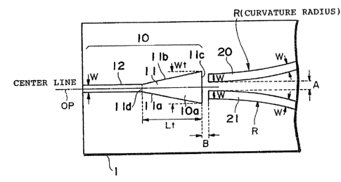
The waveguide type optical branching device of Fig. 1
comprises a substrate 1 made of a material comprising
silicon, for example, and overlying transparent material
layers (cladding member 2, and core members 10, 20 and 21)
composed of, e.g. SiOz (glass, silica glass) . That is,
these transparent material layers comprise the cores 10, 20
and 21 with higher refractive indexes than the cladding 2.
The transparent material layers comprise a non-branch
waveguide 10 , two separate branch waveguides 20 , 21, and a
cladding 2 with a lower refractive index than the core 10
embedded therein. The waveguides 10, 20 and 21 all are
arranged in the direction of propagation of light.
The non-branch waveguide 10 discussed here has a
tapered waveguide 11 at the end of a straight waveguide 12.
.. . 2134693
SE I 94-3 7
Both the branch waveguides 20, 21 are bent waveguides of
given widths and curvature radii, facing the edge face llc
of the tapered waveguide 11 at a given space.
For a more detailed explanation of the structure shown
in Fig.l, as shown in Fig. 2A and Fig. 3, the branch
waveguides 20 , 21 are bent waveguides of given widths ( Ws )
and curvature radii (Rs ) , located close to each other at a
space (A) . They are located facing the edge face of the
tapered waveguide 11 at a given space; they are positioned
symmetrically with respect to the center line of the non-
branch waveguide 10 (an alternating long and short dash line
in Fig. 3) and so that the space therebetween increases
gradually in the direction of propagation of light.
A characteristic aspect of the waveguide type optical
branching device shown in Figs . 1-3 resides in that the
terminal width (Wt) of the tapered waveguide 11 is larger
than the total ( 2W + A) of the subtotal ( 2W ) of the terminal
widths of the branch waveguides 20, 21 near the branching
section, and the space (A) between the branch waveguides 20,
21 at the branching section. In short, Wt > 2W + A. In this
aspect, this waveguide type optical branching device is
different from the waveguide type optical branching device
shown in Fig. 12.
Since the waveguide type optical branching device of
Fig. 2A comprises the branching section with a structure
wherein the non-branch waveguide 10 is separated from the
26
.2134693
SEI 94-37
branch waveguides 20, 21, there is no need for the provision
of a sharp "wedge section" as shown in Fig. 9, allowing
easier processing of the branching section and more
excellent processing stability. In addition to this
advantage, as the terminal width of the tapered waveguide
11 is made broader as mentioned above, the electric field
distribution of guided light may be spread in the direction
of width of the tapered waveguide 11-that is, in the
direction perpendicular to that of the light propagation
for closer overlapping of the electric field distributions
before and after- optical branching.
For a more detailed explanation, in the waveguide type
optical branching devices comprising the non-branch
waveguide 10 and branch waveguides 20, 21 separated
therefrom, the greater the coupling efficiency of the
electromagnetic field of the guided light at the terminal
of the non-branch waveguide 10 near the branching section,
and the electromagnetic field of the guided light at the
terminals of the branch waveguides 20, 21 near the branching
section, the less the optical branch loss.
As described above, the waveguide type optical
branching device according to the embodiment under
discussion provide the branching section with a structure
wherein the separate waveguides are located facing to each
other, and the terminal width of the tapered waveguide 11 is
enlarged, which structure allows the spreading of the
27
ww~. 2134693
SEI 94-37
electric field distribution at the terminal of the tapered
waveguide 1l in the direction of the width of the tapered
waveguide 11. As a result, the area of the overlapped
portions of the electric fields before and after optical
branching, which contributes to an improved coupling
efficiency as compared with the device shown in Fig. 1.
The above-noted device will be explained hereunder in
further detail.
The waveguide type optical branching device according
to the present embodiment comprises a silicon substrate 1,
a cladding member 2 formed on the supporting substrate 1, a
first core member ( first tapered waveguide ) 10 , a second
core member ( second waveguide ) 20 , and a third core member
(third waveguide) 21.
The first core member 10 is embedded in the cladding
member 2. The second core member 20 is embedded in the
cladding member 2 as well. Also, the second core member 20
has a second edge face 20c facing the edge face ilc of the
first core member 10 at a first space B. The third core
member 21 is also embedded in the cladding member 2. The
third core member 21 has a third edge face Zlc facing the
edge face llc of the first core member 10 at a second space
B. Here, the first space B and the second space B are
designed to be identical . The space B ( 1 ) between the edge
faces lic and 20c, and the space B ( 2 ) between the edge faces
lic and 21c have a following equation.
28
2s
SEI 94-37
B(2)-~. < B(1) 5 B(2)+~,,
where ~, is wavelength of the guided light traveling through
the core member 10 . Then the space B ( 1 ) is substantially
equal to B(2) . The wavelength ~, of the guided light using
in present embodiment is 1.55 ~,m. In other words, the first
space B ( 1 ) is not greater than the total of the space of
said second space B ( 2 ) and the wavelength ( ~, ) of the light
propagated in said second core member 20, and not smaller
than the difference between said second space B( 2 ) and the
wavelength (.1 ) of the light propagated in said second core
member 20.
The cladding member 2 (cladding 2, cladding layer 2) has
a first surface 2a. The first surface 2a is parallel to the
main surface la ( interface 1a between the substrate 1 and
cladding 2 ) of the substrate 1. "Direction of the width"
is defined to be the direction perpendicular to both the
direction perpendicular to the first surface 2a, and to the
direction of light propagation. "Direction of the
thickness" is defined to be the direction perpendicular to
the first surface 2a . The first core member 10 has a light
transmission path 12 of given width and thickness, and a
core section 11, which is contiguous with the light
transmission path 12, of a tapered type whose width
increases as the distance from the light transmission path
12 does. The width 12 of the light transmission path 12 is
defined by the distance between the side 12a and side 12b in
29
2134693
SEI 94-37
Fig. 2A. These side faces 12a and 12b are parallel to each
other.
The first core member 10 has a first perpendicular
section 12d which is def fined by intersection with a f first
plane (plane indicated by the arrows B-B in Fig. 2A) which
is perpendicular to the f first surface 2a and to an optical
axis OP of the first cladding member 10. The planes defined
by the arrows B-B through F-F are parallel to each other.
The f first core member 10 has a second perpendicular section
12e which is defined by intersection with a second plane
(plane indicated by the arrows C-C in Fig. 2A) perpendicular
to the first surface 2a and located between the fist edge
face 11c and f first plane (B-B plane ) . The f first core member
10 has a f first horizontal section ( 10a in Fig. 2A) which is
defined by intersection with a third plane (plane indicated
the arrows H-H in Fig. 1) parallel to the first surface 2a.
The second core member 20 has a third perpendicular
section 20e which is def fined by intersection with a fourth
plane (plane indicated by the arrows E-E in Fig. 2A) which
is perpendicular to the first surface 2a. The second core
member 20 has a second horizontal section (20f in Fig. 2A)
which is defined by intersection with the third plane (H-H
plane ) . The third core member 21 has a fourth perpendicular
section 21e which is defined by intersection with the fourth
plane (E-E plane) . The third core member 21 has a third
horizontal section 21f which is defined by intersection
r
2i3~s~3
SEI 94-37
with the third plane (H-H plane) .
In other words, the branch waveguide assembly shown in
Figs . 1-3 comprises a substrate 1, a first tapered waveguide
10, a second waveguide 20, and a third waveguide 21.
The substrate 1 has a substrate surface 1a.
The f first tapered waveguide 10 is formed on the
substrate surface la, and has a first edge face 11c.
The second waveguide 20 is formed on the substrate
surface la. The second waveguide 20 has a second edge face
20c facing the first edge face 11c at a given space B, a
first side 20a including a plane 20a crossing the substrate
surface la, and a second side 20b facing the first side 20a,
and the first side face 20a and the second side face 20b are
parallel to each other.
The third waveguide 21 is formed on the substrate
surface 1a. The third waveguide 21 has a third edge face
21c facing the first edge face llc at a given space B, a
third side 21a including the place 21a crossing the
substrate surface la, and a fourth side 21b facing the third
side 21a. The third side face 21a and the fourth side face
21b are parallel to each other. The fourth side 21b is
located between the first side 20a and the third side 21a.
The first side 20a is located between the second side 20b
and the fourth side 21b. The side 20a and the side 21b are
parallel to each other.
The width of the f first edge face 1a is identical to the
31
2134693
SEI 94-37
length of the first edge face la along the direction
(direction of the width) perpendicular to both the
direction of the normal to the substrate surface la
(direction of the thickness), and the direction of the
normal to the first edge face ilc (direction of the optical
axis ) . The width ( Wt ) of the first edge face l lc is greater
than the distance between the second side 20c and the third
side 21c.
In other words, an intersection (cross line) 20i is an
intersection of the second edge face 20c and second side
face 20b. An intersection (cross line) 21i is an
intersection of the third edge face 21c and third side face
21a.
An intersection ( cross line ) 20 j is an intersection of
the second edge face 20c and first side face 20a. An
intersection (cross line) 21j is an intersection of the
third edge face 21c and fourth side face 21b. An
intersection (cross line) lli is an intersection of the
first edge face llc and the side face lib. An intersection
( cross line ) 11 j is an intersection of the first edge face
ilc and the side face 11a. The distance between the line ili
and 11 j is Wt ( ~zm) , the distance between the line 20 i and
21j is (2W + A) (pm), distance Wt is greater than (2W + A).
The first core member 10 is located so that the light
input into the first core member 10 through the edge face
12c is propagated in the direction along the f first
32
' X134693
SEI 94-37
horizontal section 10a across the first perpendicular
section 12d and second perpendicular section 12e, and
output from the first edge face 11c.
The second core member is located so that the output
light from the first edge face llc is input into the second
core member 20 through the second edge face 20c, and is
propagated in the direction along the second horizontal
section 20f across the third perpendicular section 20e, and
output at the second edge face 20d of the second core member
20. The third core member 21 is located so that the output
light from the first edge face is input into the third core
member 20 through the third edge face, and is propagated in
the direction along the third horizontal section across the
fourth perpendicular section, and output from the third
core member.
In this connection, the area of the first edge face llc
is larger than the area of the first perpendicular section
I2d. This is because the first core member 10 has a tapered
section 1l which diverges toward the direction of the second
and third core members. The tapered section 11 has sides
11a, lib which forms given angles with the optical axis OP
(center line) of the first core member 10. In other words,
the tapered section 11 forms given angles with the two
surfaces perpendicular to the first surface 2a of the
section 11, while the lines 11a, 11b crossing the third
plane (H-H plane) form given angles with the optical axis OP
33
2134693
SEI 94-37
( center 1 fine ) of the f first core member 10 . As the f first
core member 10 comprises the tapered section 11, the density
of the energy (power) of the optical signal input into the
first core member 10 at the edge face 12c decreases
gradually as the light travels passing through the first
perpendicular section 12d toward the first edge face llc.
The output light from the edge face llc of the first
core member 10 is input into the second core member 20 at
the second edge face 20c, and into the third core member 2I
at the third edge face 21c. The present inventors have
found, based on their previous research, that for the
improvement in coupling efficiency of light propagated
between two optical components it is effective to make the
opposing edge faces of the respective optical components
perpendicular to the direction of light propagation. The
first edge face llc according to the present embodiment is
perpendicular to the direction of movement of the light
passing through the first edge face. Also, the second edge
face 20c is perpendicular to the direction of movement of
the incident light to the second edge face 20c. The third
edge face 21c is perpendicular to the direction of movement
of the incident light to the third edge face Zlc. As a
result, the first edge face 11c is opposite to the second
edge face 20c, whereas the first edge face llc is parallel
to the second edge face 20c. The first edge face llc is
opposite to the third edge face 21c, whereas the first edge
34
2134693
SET 94-37
face 11c is parallel to the third edge face 21c.
The second core member 20 has sides 20a, 20b
perpendicular to the first surface 2a. The side 20a and
side 20b are parallel to the direction of movement of the
light propagated in the second core member 20. In this
connection, the side 20a and side 20b faces each other,
while the side 20a and side 20b runs in parallel with each
other. Accordingly, the sides 20a and side 20b are
perpendicular to both the first surface 20a and the second
edge face 20b.
Similarly, the third core member 21 has sides 21a, 21b
which are perpendicular to the first surface 2a. The side
21a and side 21b axe parallel to the direction of movement
of the light propagated in the third core member 21. In
turn, the side 21a and side 21b are opposite to each other,
whereas the side 21a and side 2Ib are parallel to each
other. Thus, the side 21a and side 21b are perpendicular to
both the first surface 2a and third edge face 21c.
The distance between the second core member 20 and the
third core member 21 increases as their distance from the
f first core member 10 does . This is because the second core
member 20 comprises bent sides 30a, 30b bending apart from
the third core member 21. The bent side 30a is adjacent to
the plane 20a, whereas the bent side 30b to the plane 20b.
The curvature radius of the bent side 30a is R, and also the
curvature radius of the bent side 30b is almost R. The
213693
SEI 94-3 7
third core member 21 has bent sides 31a, 31b bending apart
from the second core member 20. The bent side 31a is
adjacent to the plane 21a, whereas the bent side 31b to the
plane 21b. The curvature radius of the bent side 31a is R,
and also the curvature radius of the bent side 31b is almost
R. The second core member 20 and the third core member 21
are S-shaped waveguides .
The light output from the second edge face 20c and input
into the second core member 20 is then output through the
edge face 20d of the second core member 20. The light
output from the third edge face 21c and input into the third
core member 21 is then output through the edge face 21d of
the third core member 21. In this connection, the optical
distance from the input edge face 20c to the output edge
face 20d of the second core member 20 is equal to the
optical distance between the input edge face 21c and the
output edge face 21d of the third core member 21. As a
result, in cases where beams of the light input from the
first core member 10 into the core members 20, 21 are output
from the core members 20, 21, the beams of the light
branched by the core members 20, 21 are irz the same phase
upon output from the edge faces 20d, 21d. Since the beams
of the output light from the edge faces 20d, 21d are in one
phase, the phase matching of the respective beams are easy
to perform for coupling of the output light, etc.
Fig. 4 shows a modification of the optical branching
36
2134693
SEI 94-37
device shown in Fig. 2A with improvements made on the edge
faces 20d, 21d of the second core member 20 and third core
member 21. The edge faces 20d, 21d of the optical branching
device shown in Fig. 2A is exposed. The direction of the
normal to the exposed edge face 20d forms a given angle with
the direction of movement of the light (direction of the
optical axis ) propagated in the third core member 21. Also,
the direction of the normal to the exposed edge face 21d
forms a given angle with the direction of movement of the
light propagated in the third core member 21. As mentioned
above, the present inventors have noted, based on their
previous research, that for the improvement in coupling
efficiency of light propagated between two optical
components it is effective to make the opposing edge faces
of the respective optical components perpendicular to the
direction of light propagation (direction of the optical
axis) . For this finding, as shown in Fig. 4, the optical
branching device according to the present embodiment is
positioned so that the output edge face 20d of the second
core member 20 is perpendicular to the optical axis OP2
( indicated by an alternating long and short dash line ) of
the second core member 20. Optical fiber F2 is located
opposite to the edge face 20d of the second core member 20
via a lens L2. The optical axis OP2 of the waveguide 20
corresponds to the optical axis OP2 of the fiber F2.
Additionally, the third core member 21 is located so that
37
r
2134693
SEI 94-37
the output edge face 21d of the third core member 21 is
perpendicular to the optical axis OP3 ( indicated by an
alternating long and short dash line) of the third care
member 2I. Optical fiber F3 is located opposite to the edge
face 21d of the third core member 21 via a lens L3. The
optical axis OP3 of the waveguide 21 corresponds to the
optical axis OP3 of the fiber F3. Additionally, the first
core member 10 is located so that the input edge face 12c of
the first core member 10 is perpendicular to the optical
axis OP1 ( indicated by an alternating long and short dash
line) of the first core member 21. Optical fiber F1 is
located opposite to the edge face 12c of the first core
member 10 via a lens L1. The optical axis OPl of the
waveguide 10 corresponds to the optical axis OP1 of the
f fiber F3 .
Fig. 5 is an optical branching device assembly with a 1
x 4 structure which consists of 3 connected optical
branching devices BR1, BR2 and BR3 of the type shown in Fig.
4. This optical branching device assembly comprises the
first optical branching device BR1, the second optical
branching device BR2 whose input edge face 12c is connected
to the output edge face 20d of the first optical branching
device BR1, and the third optical branching device BR3 whose
input edge face 12c is connected to the output edge face 21d
of the first optical branching device BR1.
The optical signal OS1 ( indicated by a solid arrow in
38
2134693
SEI 94-37
the drawing) input into the first optical branching device
BR1 through the edge face P1 is divided with this optical
branching device, and output through the edge faces P2, P3
of the second optical branching device BR2, and through the
edge faces P4, P5 of the third optical branching device BR3.
Conversely, the respective optical signals (indicated by
alternating long and short dash arrows ) input at the edge
faces P2-P5 are coupled with the optical branching device,
and output from the edge face P1.
Fig. 6 is an optical branching device assembly with a 1
x 8 structure which consists of 7 connected optical
branching devices BR1, BR2 , BR3 , BR4, BR5 , BR6 and BR7 of
the type shown in Fig. 4. This optical branching device
assembly comprises the first optical branching device BRl
with an input edge face ( input port ) , the second optical
branching device BR2 whose input edge face 12c is connected
to the output edge face 20d of the first optical branching
device BR1, and the third optical branching device BR3 whose
input edge face 12c is connected to the output edge face 21d
of the first optical branching device BR1.
In addition, this optical branching device assembly
comprises the fourth optical branching device BR4 whose
input edge face 12c is connected to the output edge face 20d
of the second optical branching device BR2, the fifth
optical branching device BR5 whose input edge face 12c is
connected to the output edge face 21d of the second optical
39
2134693
SEI 94-37
branching device BR1, the sixth optical branching device
BR6 whose input edge face 12c is connected to the output
edge face 20d of the third optical branching device BR3, and
the seventh optical branching device BR7 whose input edge
face 12c is connected to the output edge face 21d of the
third optical branching device BR3.
Accordingly, this optical branching device assembly may
branch single light beam input into the assembly, into eight
beams, and reversely may couple eight beams input into this
assembly into single beam. In this connection, all the
optical branching devices BR1, BR2, BR3, BR4, BRS, BR6, and
BR7 are formed on the same substrate 1.
Next, an explanation will be made regarding
optimization of the shape of the optical branching device
described with reference to Figs . 1-3 .
Fig. 7B is an illustration extractive of Figs. 1-3,
which shows only the f first core member 10 , second core
member 20 and third core member 21 of the optical branching
device assembly shown in Figs . 1-3 . Fig. 7B includes
coordinate axes. Fig. 7A is a graph showing the electric
field distribution of guided light at the terminal of the
first core member 10 or at the coordinate Yl, and the
electric ffield distribution of guided light at the
terminals of the second and third core members 20 , 21 or at
the coordinate Y2, shown in Fig. 7H. In Fig. 7A, the
electric field distribution of guided light at the
X134693
SE I 94-3 7
coordinate Y1 is shown by a solid line, whereas the electric
field distribution of guided light at the coordinate Y2, by
a dotted line. The coordinates X1 and X2 shown in Fig. 7A
correspond to the position coordinates Xl and X2 of Fig. 7B.
Here "guided light" means light propagated through the core
members 10, 20 and 21 of the optical branching device in
question. Each distribution shown in Fig. 7A is normalized
so that the optical power carried in each waveguide mode is
set at 1. Here, it is assumed that excitation is effected
only in the lowest mode in either of the non-branch
waveguide 10 and branch waveguides 20, 21.
In the optical branching device assembly according to
the present embodiment, the length (Wt) of the intersection
of the first horizontal section 10a and first edge face 11c
is greater than the total of the length (W1 ) of the
intersection of the second horizontal section 20f and
second edge face 20c, the length (W2) of the third
horizontal section 21f and third edge face 21c, and the
distance (A) between the second edge face (20c) and third
edge face ( 21c ) . More precisely, the distance between the
side face 20a and side face 21b is A. In other words, the
distance between the line 21 j and 20 j is A.
That is, Wt is larger than W1 + W2 + A. In short, Wt >
Wl + W2 + A. Incidentally, in the present embodiment, W1 =
W2 = W.
Fig. 10 shows the electric field distribution of the
41
2134fi93
SEI 94-37
comparison optical branching device assembly shown in Fig.
11. In the optical branching device assembly shown in Fig.
11, the terminal width (Wt) of the tapered waveguide added
to the straight waveguide 12 is equal to the total (2W + A)
of the subtotal (2W) of the widths of the branch waveguides
20, 21 (each W in the case of Fig. 11), and the direction (A)
between the branch waveguides 20, 21 at the branching
section.
Fig. 10B is an illustration extractive of Fig. 10, which
shows only the first core member 10, second core member 20
and third core member 21 of the optical branching device
assembly shown in Fig. 11. Fig. 10B includes coordinate
axes.
Fig. 10A is a graph showing the electric field
distribution of guided light at the terminal of the first
core member IO or at the coordinate Yl , and the electric
field distribution of guided light at the terminals of the
second and third core members 20, 21 or at the coordinate
Y2, shown in Fig. 10B. In Fig. 10A, the electric field
distribution of the guided light at the coordinate Yl is
shown by a solid line, whereas the electric field
distribution of the guided light at the coordinate Y2, by a
dotted line. The coordinates X1 and X2 shown in Fig. 10A
correspond to the position coordinates Xl and X2 of Fig.
10B, respectively. Here "guided light" means light
propagated through the core members 10 , 20 and 21 of the
42
X134693
SEI 94-37
optical branching device in question. Each distribution
shown in Fig. 7A is shown normalized so that the optical
power is set at 1. Here, it is assumed that excitation is
effected only in the lowest mode in either of the non-branch
waveguide 10 and branch waveguides 20, 21.
As mentioned above, the optical branching device shown
in Fig. 7A and Fig. 7B has a larger width (Wt) of the first
edge face llc of the tapered section 11 than the optical
branching device shown in Fig. 10A and Fig. 10B, related to
the dividing waveguide 20, 21.
As Fig. 7A shows, with the increased terminal width (Wt)
of the tapered waveguide 11, the electric field
distribution at the terminal of the tapered waveguide 11
spreads in the direction of the width of the tapered
waveguide 11, providing a larger area of the overlapped
portions of the electric fields before and after optical
branching. As a result, there is an improvement in the
coupling efficiency resulting from the overlap integral of
the electric field distributions before and after optical
branching. With this improvement, the radiation of guided
light between the branch waveguides 20, 21 is suppressed,
leading to a reduced optical branch loss as compared with
the comparison waveguide type optical branching device.
As explained above, it has been revealed that the
optical branching device shown in Figs . 7A and 7B which
satisfies the relationship: wt > W1 + W2 + A provides a
43
2134693
SEI 94-37
higher optical coupling efficiency than the optical
branching device shown in Figs . 10A and lOB which satisfies
the relationship: Wt = W1 + W2 + A.
The position of the peak P1 of the electric field at end
face 20c corresponds to the optical axis OP2 of the second
waveguide 20, and the position of the peak P1 of the
electric field at end face corresponds to the optical axis
OP3 of the third waveguide 21. The distance Wp-p between the
peaks PI and P2 is greater than 2 (um) and smaller than Wt
(gym), where Wt is the width of the first edge face.
Next, in order to further increase the optical coupling
efficiency, the optical branching device stands in need for
further improvement.
Fig. 8 is a graph showing the relationship between the
width ( Wt ) at the terminal of the tapered waveguide 11 and
the excess branch loss (dB) of the optical branching device
shown in Figs . 1-3 . Particularly, Fig. 8 shows a graph
representing the results of calculation of the excess
branch loss at a wavelength of guided light of 1.55 ~m while
changing the width (Wt) at the terminal llc of the tapered
waveguide 11. Here, the excess branch loss was calculated
by the beam propagation method. For this calculation, the
dimensions of the respective parts of the waveguide type
optical branching device shown in Fig, 2A and Fig. 3 were
set as A = 4 Vim, B = 4 Vim, W = 8 Vim, Lt = 1200 Vim, and R = 50
mm, and the specific refractive index difference between
44
2134693
SE I 94-3 7
the core and cladding at 0 . 3 0 . B stands for the distance
between the second edge face 20c of the second core member
20 and the first edge face 11c of the first core member 10.
It is noted that B is substantially equal to the distance
between the third edge face 21c of the third core member 21,
and the first edge face lic of the first core member 10. Lt
stands for the distance between the edge face llc of the
tapered section 1l, and the interface lid between the
tapered section 11 and the straight section 12, shown in
Fig. 3 .
To suppress the loss to a satisfactory degree while
maintaining favorable processing stability, preferably the
distance (A) between the branch waveguides 20, 21 at the
branching section is about 2-4 Vim, and the distance (B)
between the non-branch waveguide 10 and the branch
waveguides 20, 21 facing it is desired to be about 2-8 Vim.
According to the graph shown in Fig. 8, a minimum loss
of 0. 27 dB is accomplished in the case where the width (Wt)
of the terminal 11c of the tapered waveguide 11 is 6 ~m
greater than 20 ~m which is the total ( 2W + A) of the
subtotal ( W + W ) of the widths ( Ws ) of the terminals 20c,
21c of the branch waveguides 20, 21, and the distance (A)
between the branch waveguides Z0, 21-that is, in the case of
Wt = 26 Vim. The excess branch loss of the optical branching
device scaled to Wt = 20 ~m is 0.42 dB, whereas the excess
branch loss of the optical branching device scaled to Wt =
2134693
SEI 94-37
26 ~m is 0.27 dB. Accordingly, the optical branching device
shown in Figs 7A and 7B provides a considerable reduction in
the loss as compared with the optical branching device with
the non-increased width of the terminal llc which is shown
in Fig. 10A and Fig. 10B, and suffers from an increased loss
of 0.42 dB.
If the width (Wt) of the terminal 11c of the tapered
waveguide 11 is enlarged excessively, the radiation of
guided light through the enlarged terminal section 11
(described later) increases with a greater loss of the
light. In summary, as the graph shown in Fig. 7 suggests,
the enlarged width (wt) of the terminal 11c of the tapered
waveguide 11 is desired to be about 10 ~m or less . For long-
distance optical communication, the excess branch loss is
desired to be 0.3 dB or less. In conclusion, desirably the
width (Wt) of the terminal 11c is greater than 23
micrometers, but smaller than 29 micrometers.
Particularly, in the case where the terminal width ( Wt ) of
the tapered waveguide 11 is about 25-27 ~m ( the increased
terminal width is about 5-7 Vim) , the excess branch loss
converges on a constant value of 0.27 dB. Therefore, for a
maximum loss reduction, desirably the width (Wt) of the
terminal llc is larger than 25 micrometers, but smaller than
27 micrometers.
Hereunder, an optical branching device according to
another embodiment of the present invention will be
46
X134693
SEI 94-37
explained.
Fig. 12 is a perspective view of an optical branching
device according to another embodiment of the present
invention.
Fig. 13A is a section view of this device, taken along
the plane indicated by the arrows H-H in Fig. 12.
Fig. 13B is a section view of the device shown in Fig.
13A, taken along the plane indicated by the arrows B-B in
the drawing.
Fig. 13C is a section view of the device shown in Fig.
13A, taken along the plane indicated by the arrows C-C in
the drawing.
.Fig. 13D is a section view of the device shown in Fig.
13A, taken along the plane indicated by the arrows D-D in
the drawing.
Fig. 13E is a section view of the device shown in Fig.
13A, taken along the plane indicated by the arrows E-E in
the drawing.
Fig. 13F is a section view of the device shown in Fig.
13A, taken along the plane indicated by the arrows F-F in
the drawing.
Fig. 13G is a section view of the device shown in Fig.
13A, taken along the plane indicated by the arrows G-G in
the drawing.
Fig. I4 is a section view of the device shown in Fig.
13A.
47
2134693
SEI 94-37
This waveguide type optical branching device comprises,
at the terminal llc of the tapered waveguide 11 of the
waveguide type. optical branching device shown in Fig. 1, a
tapered waveguide 115 with a structure constructed by
addition to the terminal ilc of the tapered section 11 of a
straight section 116 of almost the same width.
With this structure, the guided light whose wave front
has spread radially in the tapered section 115 may be input
into branch waveguides 120, 121 after being restored to a
plane.
Fig. 15 illustrates the manner of travelling of the wave
front. The above-noted restoration contributes to the
suppressed radiation (reflection, diffraction) of guided
light at the section of the edge face of the tapered
waveguide 111 near the branching section which is provided
for increasing the terminal width ( the section having a
width larger than the total of the terminal widths of the
branch waveguides 120, 121, and the distance between the
branch waveguides 120, 121), thereby enabling a further
reduction in the radiation loss at the branching section.
A more detailed explanation will be made regarding the
optical branching device according to the present
embodiment.
As Fig. 12 shows, the waveguide type optical branching
device according to the present embodiment comprises a
silicon substrate 101, a cladding member 102 formed on the
48
ur. 2134693
SEI 94-37
supporting substrate 101, a f first core member ( f first
tapered waveguide ) 110, a second core member ( second
waveguide) 120, and a third core member (third waveguide)
121.
The first core member 110 is embedded in the cladding
member 102. The second core member 120 is embedded in the
cladding member 102 as well. Also, the second core member
120 has a second edge face 120c facing the edge face lllc of
the f first core member 110 at a f first space B . The third core
member 121 is also embedded in the cladding member 102. The
third core member 121 has a third edge face 121c facing the
edge face 111c of the f first core member 110 at a second
space B . Here, the f first space B and the second space B are
des igned to be identical . The space B ( 1 ) between the edge
faces laic and 120c, and the space B ( 2 ) between the edge
faces 111c and 121c have a following equation.
B(2)-~, <_ B(1) 5 B(2)+7l,
where ~, is wavelength of the guided light traveling through
the core member 110 . Then the space B ( 1 ) is substantially
equal to B( 2 ) . The wavelength .1 of the guided light using
in present embodiment is 1.55 Vim. In other words, the first
space B ( 1 ) is not greater than the total of the space of
said second space B ( 2 ) and the wavelength ( ~, ) of the light
propagated in said second core member 120, and not smaller
than the difference between said second space B ( 2 ) and the
wavelength ( ~. ) of the light propagated in said second core
49
- 2134693
SE I 94-3 7
member 120.
The cladding member 102 (cladding 102, cladding layer
102) has a first surface 102a. The first surface 102a is
parallel to the main surface 101a of the substrate 101. The
main surface 101a is defined by the interface between the
cladding member 102 and substrate 101. "Direction of the
width" is defined to be the direction perpendicular to both
the direction perpendicular to the first surface 102a, and
to the direction of light propagation. "Direction of the
thickness" is defined to be the direction perpendicular to
the first surface 102a. The first core member 110 has a
light transmission path 112 of given width and thickness,
a core section 115, which is contiguous with the light
transmission path 112, of a tapered type whose width
increases as the distance from the light transmission path
112 does, and a second core section 116 adjacent to the core
section 1I5.
The width 112 of the light transmission path 112 is
defined by the distance between the side ll2a and side 112b
in Fig. 13A.
The f first core member 110 has a f fifth perpendicular
section 112d which is def fined by intersection with a plane
(plane indicated by the arrows B-B in Fig. 13A) which is
perpendicular to the first surface 102a.
The first core member 110 has a first perpendicular
section 112e which is defined by intersection with a first
2134693
SEI 94-37
plane (plane indicated by the arrows C-C in Fig. 13A)
perpendicular to the first surface 102a.
The first core member 110 has a second perpendicular
section 116c which is defined by intersection with a second
plane (plane indicated by the arrows G-G in Fig. 13A)
perpendicular to the first surface 102a and located between
the first edge face 111c and first plane (B-B plane) .
The first core member 110 has a first horizontal section
(110a in Fig. 13A) which is defined by intersection with a
third plane (plane indicated the arrows H-H in Fig. 1 )
parallel to the first surface 102a.
The second core member 120 has a third perpendicular
section 120e which is defined by intersection with a fourth
plane (plane indicated by the arrows E-E in Fig. 13A) which
is perpendicular to the first surface 102a. The second core
member 120 has a second horizontal section ( 120f in Fig.
13A) which is defined by intersection with the third plane
(H-H plane) . The third core member 121 has a fourth
perpendicular section 121e which is defined by intersection
with the fourth plane ( E-E plane ) . The third core member
121 has a third horizontal section 121f which is defined by
intersection with the third plane (H-H plane) .
The first core member 110 is located so that the light
input into the first core member 110 through the edge face
112c is propagated in the direction along the first
horizontal section 110a across the first perpendicular
51
X134693
SEI 94-37
section 112e and second perpendicular section 116c, and
output from the first edge face lilc.
Here, it is assumed that the sections are parallel to
the f first edge face 111c, and perpendicular to the direction
of movement of guided light.
The second core member 120 is located so that the output
light from the first edge face 111c is input into the second
core member 120 through the second edge face.120c, and is
propagated in the direction along the second horizontal
section 120f across the third perpendicular section 120e,
and output at the second edge face 120d of the second core
member 120. The third core member 121 is located so that
the output light from the first edge face is input into the
third core member 121 through the third edge face 121c, and
is propagated in the direction along the third horizontal
section 121f across the fourth perpendicular section 121e,
and output f rom , the third core member 121.
In this connection, the area of the first edge face lllc
is larger than the area of the f first perpendicular section
112e . This is because the f first core member 110 has a
tapered section 115 which diverges toward the direction of
the second and third core members 120 , 121. The tapered
section 115 has sides 115a, 115b which form given angles
with the optical axis OP1 ( center line ) of the f first core
member 110. Tn other words, the intersections 115a, 115b
between the two surfaces 115a, 115b perpendicular to the
52
2134fi93
SEI 94-37
first surface 102a of the section 115, and the lines 115a,
115b crossing the third plane (H-H plane) form given angles
AGl with the optical axis OP1 (center line) of the first
core member 1I0 in the third surface (H-H plane) .
In other words, this branch waveguide comprises a
substrate 101 with a substrate surface lOla, a first tapered
waveguide 110, a second waveguide 120 and a third waveguide
121.
The first tapered waveguide 110 comprises a fourth
waveguide 116, and a second tapered waveguide 115 which is
ad j acent thereto . The first tapered waveguide 110 is formed
on the substrate surface la.
The fourth waveguide 116 has a first edge face 111c
including a plane which crosses the substrate surface la,
a fifth side 116a including a plane which crosses the
substrate surface la, and a sixth side lllc parallel to the
fifth side 116a.
The second tapered waveguide 115 is contiguous with the
fourth waveguide (straight waveguide) 116. The second
tapered waveguide 115 diverges toward the fourth waveguide
116. The second waveguide 120 is formed on the substrate
surface la. The second waveguide 120 has a second edge face
120c facing the first edge face 111c at a given space.
The third waveguide 121 is formed on the substrate
surface lOla. The third waveguide 121 has a third edge face
121c facing the first edge face lllc at a given space. As
53
- 2134693
SEI 94-3 7
the first core member 110 comprises the tapered section 115,
the density of the energy (power) of the optical signal
input into the first core member 110 at the edge face 112c
decreases gradually as the light travels passing through
the f first perpendicular section 112d toward the f first edge
face 111c .
The output light from the edge face lllc of the first
core member 110 is input into the second core member 120
through the second edge face 120c, and into the third core
member 121 through the third edge face 121c. The present
inventors have found, based on their previous research,
that for the improvement in coupling efficiency of light
propagated between two optical components it is effective
to make the opposing edge faces of the respective optical
components perpendicular to the direction of light
propagation. The first edge face lllc of the optical
branching device according to the present embodiment is
perpendicular to the direction of movement of the light
passing through the first edge face lllc. Also, the second
edge face 120c is perpendicular to the direction of movement
of the incident light to the second edge face 120c. The
third edge face 121c is perpendicular to the direction of
movement of the incident light to the third edge face 121c.
As a result, the first edge face lllc is opposite to the
second edge face 120c, whereas the first edge face 111c is
parallel to the second edge face 120c. The first edge face
54
2134693
SEI 94-37
lllc is opposite to the third edge face 121c, whereas the
first edge face lllc is parallel to the third edge face
l2ic.
For a further improvement in the optical coupling
efficiency of the optical branching device, the area of the
second perpendicular section 116c is made identical to the
area of the first edge face lllc for the optical branching
device according to the present embodiment. In other words,
the width of the second perpendicular section 116c is
identical to the width ( Wt ) of the first section lllc .
More particularly, as shown in Fig. 15, the light input
into the first core member 110 gradually loses its optical
power density (energy density) as it travels from the first
perpendicular section 112e to the first edge face 111c,
while the wave front of the light fans out in the first
horizontal section 110a. In the case where the area of this
second perpendicular section 116c is equal to the area of
the first edge face lllc, the wave front becomes parallel to
the first edge face during its propagation from the second
perpendicular section 116c to the first edge face 111c.
As a result, the directivity of the light output from
the first edge face 111c is increased, which results in an
increased coupling efficiency of the light entering the
second core member 120 and third core member 121.
In addition, as the second edge face 120c and third edge
face 121c are parallel to the wave front WA2 leaving the
2~346~3
SE I 94-3 7
first edge face lllc, the optical coupling efficiency is
increased.
In summary, the first core member 110 has the first edge
face lllc which aids in lowering the energy density of the
input light, and is in the form which makes the wave front
WAl of the light parallel to the first edge face illc for
its exit through the first edge face lllc. The second core
member 120 has the second edge face 120c facing the first '.
edge face 111c at a given space, and the third core member
121c has a third edge face 121c facing the first edge face
111c at a given space ( B ) .
The light travels through the light transmission path
( core ) 112 of a given width ( core size ) . The light
transmission path 112c is a part of the first core member
110 which is adjacent to the tapered waveguide 115, and has
the same sectional area as the minimum sectional area of the
first perpendicular section 112e.
The second core member 120 has sides 120a, 120b
perpendicular to the f first surface 102a and to the second
edge face 120c. The side 120a and side 120b are parallel to
the direction of movement of the light propagated in the
second core member 120. In this connection, the side 120a
and side 120b faces each other, while the side 120a and side
120b run in parallel with each other. Accordingly, the sides
120a and side 120b are perpendicular to both the first
surface 102a and the second edge face 120b.
56
2134693
SE I 94-3 7
Similarly, the third core member 121 has sides 121a,
121b which are perpendicular to the first surface 102a. The
side 121a and side 121b are parallel to the direction of
movement of the light propagated in the third core member
121. In turn, the side 121a and side 121b are opposite to
each other, whereas the side 121a and side 121b are parallel
to each other . Thus , the side 121a and s fide 121b are
perpendicular to both the f first surface 102a and third edge
face 121c.
The width (Wt) of the first edge face 111c is greater
than the distance between the second side 120c and the third
side 121c.
In other words, an intersection (cross line) 120i is an
intersection of the second edge face 120c and second side
face 120b . An intersection ( cross line ) 1211 is an
intersection of the third edge face 121c and third side face
121a.
An intersection (cross line) 120j is an intersection of
the second edge face 120c and first side face 120a. An
intersection (cross line) 121j is an intersection of the
third edge face 121c and fourth side face 121b. An
intersection (cross line) IIIi is an intersection of the
first edge face 111c and the side face lllb. An intersection
( cross line ) 111 j is an intersection of the f first edge face
111c and the side face 111a. The distance between the line
111i and 111j is Wt (pm), the distance between the line 1201
57
2~34fi93
SEI 94-37
and 121 j is ( 2W + A) ( pm) , distance Wt is greater than ( 2W
+ A) . The distance between the side face 20a and side face
21b is A. In other words, the distance between the line 21 j
and 20 j is A.
The space between the second core member 120 and the
third core member 121 increases as their distance from the
first core member 110 does . This is because the second core
member 120 comprises bent sides 130a, 130b bending apart
from the third core member 121. The bent side 130a is
adjacent to the plane 120a, whereas the bent side 130b to
the plane 120b. The curvature radius of the bent side 130a
is R, and also the curvature radius of the bent side 130b is
almost R. The third core member 121 has bent sides 131a,
131b bending apart from the second care member 120. The
bent side 131a is adjacent to the plane 121a, whereas the
bent s ide 131b to the plane 121b . The curvature radius of
the bent side 131a is R, and also the curvature radius of
the bent side I3Ib is almost R.
The light output from the second edge face 120c and
input into the second core member 120 is then output through
the edge face 120d of the second core member 120. The light
output from the third edge face 121c and input into the
third core member 121 is then output through the edge face
121d of the third core member 121. In this connection, the
optical distance from the input edge face 120c to the output
edge face 120d of the second core member 120 is equal to the
58
2134693
SEI 94-37
optical distance between the input edge face 121c and the
output edge face 121d of the third core member 121. As a
result, in cases where beams of the light input from the
first core member 110 into the core members 120, 121 are
output from the core members 120, 121, the beams of the
light branched by the core members 120, 121 are in the same
phase upon output from the edge faces 120d, 121d. Since the
beams of the output light from the edge faces 120d, 121d are
in one phase, the phase matching of the respective beams are
easy to perform for coupling of the output light, etc.
The fourth waveguide 116 has face (fifth side) 116a and
face (sixth face) 116b. These faces 116a, 116b are
substantially parallel to each other, and in other words,
the area ( S1 ) of first edge face lllc is substantially equal
ZS to the area(S2) of the second perpendicular section 116c.
The word "substantially" means as follows. The angle
between the line 116a and line 116b is less than 3 degree
and more than and equal to 0 degree . The area ( S1 ) is
greater than the area(S2)x97% and less than the
area(S2)x103%.
The optical component device shown in Fig. 15 comprises
a light input means IM, first optical detector OM1, and
second optical detector OM2. The input means IM is connected
to the edge face 112c of the f first waveguide 110 . The input
means IM comprises a light source IM1, a first input fiber
IM4 , a second input f fiber IM6 , a lens IM3 arranged between
59
2134693
SE I 94-3 7
said light source such as laser diode IM1 and said first
input fiber IM4, a lens IM5 arranged between said first
input f fiber IM4 and second input f fiber IM6 . The second input
f fiber IM6 is connected to the f first waveguide 110 at the
S edge face 112c directly. The first output detector OMI is
connected to the edge face 120d of the second waveguide 120,
through a output f fiber F102 . The output f fiber is connected
to the edge 120d of the second waveguide 120 directly. The
second output detector OM2 is connected to the edge face
IO 121d of the third waveguide 121, through a output f fiber
F102. The output fiber OM2 is connected to the edge 121d of
the third waveguide 121 directly. The light travelling
through the system is identified by signs IM2, IM7, IM12,
IM8 , IM9 , IM10 , IM11, in th is f figure .
15 Fig. 16 shows a modification of the optical branching
device shown in Fig. 13A with improvements made on the edge
faces 120d, 121d of the second core member 120 and third
core member 121. The edge faces 120d, 121d of the optical
branching device shown in Fig. 13A is exposed. The
20 direction of the normal to the exposed edge face 120d forms
a given angle with the direction of movement of the light
(direction of the optical axis) propagated in the third core
member 121. Also, the direction of the normal to the
exposed edge face 121d forms a given angle with the
25 direction of movement of the light propagated in the third
core member 121. More particularly, the second core member
f
X134693
SEI 94-37
120 and the third core member 121 are S-shaped waveguides .
As mentioned above, the present inventors have noted, based
on their previous research, that for the improvement in
coupling efficiency of light propagated between two optical
components it is effective to make the opposing edge faces
of the respective optical components perpendicular to the
direction of Light propagation (direction of the optical
axis ) . For this f finding, as shown in Fig. 16, the optical
branching device according to the present embodiment is
positioned so that the output edge face 120d of the second
core member 120 is perpendicular to the optical axis OP2
( indicated by an alternating long and short dash line) of
the second core member 120 . Optical f fiber F102 is located
opposite to the edge face 120d of the second core member 120
via a lens L102. Additionally, the third core member 121 is
located so that the output edge face 121d of the third core
member 121 is perpendicular to the optical axis OP3
( indicated by an alternating long and short dash line ) of
the third core member 121. Optical fiber F103 is located
opposite to the edge face 121d of the third core member 121
via a lens L103. Additionally, the first core member 110 is
located so that the input edge face 112c of the f first core
member 110 is perpendicular to the optical axis OP1
( indicated by an alternating long and short dash line) of
the first core member 121. Optical fiber F101 is located
opposite to the edge face 112c of the first core member 110
61
213493
SE I 94-3 7
via a lens L101. The optical axes OP1, OP2; OP3 of the
waveguide 110, 120, 121 correspond to axes OP1, OP2, OP3 of
the fiber FI01, F102, F103, respectively.
Fig. 17 is an optical branching device assembly with a
1 x 4 structure which consists of 3 connected optical
branching devices BR101, BR102 and BR103 of the type shown
in Fig. 16. This optical branching device assembly
comprises the f first optical branching device BR101, the
second optical branching device BR102 whose input edge face
112c is connected to the output edge face 120d of the first
optical branching device BR101, and the third optical
branching device BR103 whose input edge face 112c is
connected to the output edge face 121d of the first optical
branching device BR101. The optical signal (indicated by
a solid arrow in the drawing) input into the first optical
branching device BR101 through the edge face P101 is divided
with this optical branching device, and output through the
edge faces P102, P103 of the second optical branching device
BR102, and through the edge faces P104, P105 of the third
optical branching device HR103. Conversely, the respective
optical signals ( indicated by alternating long and short
dash arrows ) input at the edge faces P102-P105 are coupled
with the optical branching device, and output from the edge
face P101.
Fig. 20 is an optical branching device assembly with a
1 x 8 structure which consists of 7 connected optical
62
2134693
SEI 94'37
branching devices HR101, BR102, BR103, BR104, BR105, BR106
and BR107 of the type shown in Fig. 4. This optical
branching device assembly comprises the first optical
branching device BR101 with an input edge face ( input port) ,
the second optical branching device BR202 whose input edge
face 112c is connected to the output edge face 120d of the
first optical branching device BR101, and the third optical
branching device BR103 whose input edge face 112c is
connected to the output edge face 121d of the f first optical
branching device BR101. In addition, this optical
branching device assembly comprises the fourth optical
branching device BR104 whose input edge face 112c is
connected to the output edge face 120d of the second optical
branching device BR102, the fifth optical branching device
BR105 Whose input edge face 112c is connected to the output
edge face 121d of the second optical branching device HR101,
the sixth optical branching device BR106 whose input edge
face 112c is connected to the output edge face 120d of the
third optical branching device BR103, and the seventh
optical branching device BR107 whose input edge face 112c
is connected to the output edge face 121d of the third
optical branching device BR103.
Accordingly, this optical branching device assembly may
branch single light beam input into the assembly, into eight
beams, and reversely may couple eight beams input into this
assembly into single beam. In this connection, all the
63
2134fi93
SEI 94-37
optical branching devices BR101, BR102, BR103, HR104,
BR105, BR106, and BR107 are formed on the same substrate 1.
Fig. 18 is a graph showing the relationship between the
length Ls of the straight section 116 and the excess branch
loss . More particularly, it is a graph which represents the
results of calculation by the beam propagation method of the
excess branch loss of the optical branching device shown in
Fig. 12 for guided light at a wavelength of 1.55 Vim. For
calculation, the dimensions of the respective parts of the
waveguide type optical branching device were set to be A =
4 um, B = 4~m, W = 8~m, Lt = 1200 Vim, and R = 50 mm. The
terminal width (Wtj of the tapered section 15 is 26 Vim, the
wavelength for which a maximum loss reduction was observed
with the waveguide type optical branching device shown in
Fig. 1. The specific refractive index difference between
the core and cladding was set to be 0.3%. B is the distance
between the second edge face 120c of the second core member
120 and the first edge face lllc of the first core member
110. Here, B is equal to the distance between the third
edge face 121c of the third core member 121, and the first
edge face 111c of the first core member 110 . Ls is the
distance between the edge face 111c of the fourth waveguide
116 of the tapered section 111, and the interface between
the fourth waveguide 116 and the second tapered section 115,
shown in Fig. 14. Lt is the distance between the interface
llle, and the interface 111d between the second tapered
64
2134693
SEI 94-37
waveguide 115 and the optical waveguide 112, shown in Fig.
14.
As Fig. 18 shows, the minimum excess loss is 0.23 dB
with the waveguide type optical branching device shown in
Fig. 12. This minimum value is accomplished when the length
of the straight section 116 is about 300 Vim. The minimum
excess loss with the waveguide type optical branching
device shown in Fig. 1 is 0.27 dB. Tn conclusion, the
optical branching device shown in Fig. 12 is more excellent
than the optical branching device shown in Fig. 1. Tt has
been confirmed that the waveguide type optical branching
device shown in Fig. 12 has a greater effect on the loss
reduction.
If the straight section (fourth waveguide) 116 is
excessively long, then loss at sections other than the
branching section increases due to the occurrence of the
higher mode, etc. Therefore, the length (Ls) of the
straight section 116, or the length of the sixth side 116c
is preferred to be about 300 ~,m for which the minimum loss
is observed. In this connection, the excess branch loss
significantly lowers in cases where the length of the
straight section 116 is shorter than 400 micrometers, but
is longer than 100 Vim. Accordingly, it is desired that the
length of the third waveguide 116, or the length of the
sixth side 116b is shorter than 400 micrometers, but is
longer than 100 Vim. At a length of the straight section
X134693
SEI 94-37
116, or the length of the sixth side 116c of 300 micrometers
or less, but greater than 250 hem, the value of excess branch
loss converges on a constant value (the minimum value: 0.27
dB).
For the confirmation of the effect of the optical
branching device according to the present embodiment, the
present inventors fabricated the optical branching devices
shown in Fig. 1, Fig. 12, and Fig. 11. The present
inventors measured the light transmission properties of the
devices. The results will be given hereunder.
First experiment
The present inventors prepared the waveguide type
optical branching devices shown in Fig. 1, Fig. 12, and Fig.
11. The branch waveguide of Fig. I1 was prepared for
comparison in properties with the branch waveguide of Fig.
1 and Fig. 12. 1 x 2 structures were fabricated with these
branch waveguides.
These waveguide type optical branching devices were
prepared by forming a Si02 glass layer (cladding) on a
silicon substrate 1 or 101 by the FHD (flame hydrolysis
deposition) method, depositing a doped SiOz glass layer with
a high refractive index, forming a core by etching, and
forming a upper cladding by the deposition of a Si02 glass
layer.
The dimensions of the respective parts of the
respective devices are represented as follows using the
66
w,.2 , ~ 213693
SEI 94-37
reference characters employed in Fig.l, Fig. 12, Fig. 11.
A = 4 ~m
B = 4 ~,m
W = 8 ~,m
Lt = 1200 ~m
R = 50 mm
( The above dimens ions are common to the three types of
Figs. 1, 12, and 11. )
The terminal widths ( Wts ) of the f first tapered
waveguides and the length Ls of the straight section 16 were
different as follows:
For the type shown in Fig. 1 (an embodiment of the
present invention) , Wt = 26 Vim, Ls = 0 Vim.
For the type shown in Fig. 12 (another embodiment of the
present invention) , Wt = 26 Vim, Ls = 250 ~,m.
For the type shown in Fig. 11 (a comparison) , Wt = 20
Vim, Ls = 0 ~m .
In all the cases, the specific refractive index difference
between the core and cladding was 0.3~, and the thickness of
the waveguide was 8 Vim.
Laser diode light with a wavelength of 1.55 ~m was input
into and output from each of the above-noted waveguide type
optical branching devices through single mode fiber for
measurement of the excess branch loss . The excess branch
loss is defined to be the value calculated by subtracting
the total of the essential loss with a 1 x 2 branching
67
..... .
2134fi93
SEI 94-37
structure of 3 dB, the coupling loss with the input, output
fiber, and the transmission loss of the waveguides from the
entire loss with the optical branching device .
Ten samples were prepared for each type of device, and
averages of the measured values were taken. As a result,
the mean excess branch losses were as follows
0. 36 dB for the type of Fig. 1 (an embodiment of the
present invention);
0. 32 dB for the type of Fig. 12 (another embodiment of
the present invention); and
0. 55 dB for the type of Fig. 11 (a comparison) .
The measurement error was ~ 0.05 db. Accordingly, even if
a measurement error happened, it is noted that there exists
a significant difference between the devices according to
the present embodiments and the comparison device. It was
actually confirmed that the scaling up of the terminal width
of the first tapered waveguide 11 or 111 contributed to a
reduction in the optical branch loss .
Second experiment
The present inventors manufactured waveguide type
optical branching devices with a 1 x 8 structure shown in
Fig. 6 and Fig. 20. Further, another waveguide assembly
with a 1 x 8 structure (device as a second comparison) using
waveguides shown in Fig. 11. The second comparison device
was prepared for comparison in properties with the branch
waveguide assemblies shown in Fig. 6 and Fig. 20. The
68
2134693
SEI 94-37
present inventors measured the excess branch loss with each
device . The 1 x 8 device according to each of the
embodiments of the invention was constructed with a
structure where the terminals of branch waveguides 20, 21
( 120 , 121 ) of the 1 x 2 device according to the embodiment
of the invention were connected to the first tapered
waveguide 11 (or 111 ) of another 1 x 2 device according to
the same embodiment. The entire device comprised a
combination of a plurality of the 1 x 2 devices of each
embodiment arranged in the direction of propagation of
light.
The prepared devices are a 1 x 8 device which is a
three-stepped branching assembly of the 1 x 2 devices shown
in Fig. 1, and another three-stepped branching 1 x 8 device
comprising the devices shown in Fig. 12. The comparison 1
x 8 device was also prepared by a three-stepped combination
of the devices shown in Fig. 11.
The mean excess branch loss of guided light with a
wavelength of 1.55 ~m was measured for the output from each
of the eight output ports of each 1 x 8 device, and averages
were taken. As a result of the measurement, the mean excess
branch loss of the 1 x 8 device shown in Fig. 6 was 1.02 dB,
whereas the mean excess branch loss of the 1 x 8 device
shown in Fig. 20 was 0.89 dB. The 1 x 8 device prepared with
the devices shown in Fig. 11 (the second comparison device)
produced a mean excess branch loss of 1.53 dB. The mean
69
2134693
SEI 94-37
excess branch losses of the devices shown in Fig. 6 and Fig.
20 were less than the mean excess branch loss observed with
the device shown in Fig. 11. Thus, the superiority of the
waveguide assembly shown in Fig, 6 over the second
comparison device has been revealed experimentally. Also
the experiments have revealed that the device shown in Fig.
20 is more excellent than the device shown in Fig. 6. The
level of lowering of the mean excess branch loss with the
improved devices is much higher than the level of the
measurement error. This proves that the effect of addition
of the straight section 116 are produced in a cumulative
manner by the three=stepped combination of the 1 x 2 devices
shown in Fig. 1 and Fig. 12. As proof of this, it has been
confirmed that the optical branch loss is more effectively
reduced with the waveguide type optical branching device of
Fig. 12.
Fig. 19 is a graph showing the results of measurement of
wavelength-dependency of the excess branch loss with the 1
x 8 device shown in Fig. 20, and the second comparison 1 x
8 device. During the measurement, the incident light into
the respective devices was emitted from a spectroscope.
Referring to the graph shown in Fig. 19, it may be
confirmed that the 1 x 8 device of Fig. 20 suffers from a
Lower loss than the second comparison device over a wide
range of wavelength of guided light. In addition, the types
of the embodiments of the present invention are less
2134693
SEI 94-37
susceptible to variance in the loss depending on the guided
light width changes, as compared with the comparison type.
For this reason, the waveguide type optical branching
device according to the present invention has an additional
advantage in that it may be used satisfactorily even for
optical measurement systems which sweep light over a wide
wavelength range.
Fig. 21 shows an optical branching device comprising a
light-shielding member 140. The light shielding-member 140
is arranged between the second waveguide 120 and third
waveguide 121. The light-shielding member is for example
made of a material of which color is black. The black
material is made of black rubber and carbon graphite. The
light-shielding member can be made of a metal including Au,
Fe, Cu, Ag, Sn, Zn or solder, rubber or resign.
Hereunder, an optical branching device according to
another embodiment of the present invention will be
explained.
An optical branching device comprise waveguide present
invention is shown in Figs . 22-24 . This is a roughly Y-
shaped branching and coupling device (Y-shaped device) for
branching or coupling guided light transmitted along the
single mode waveguide 312 or 320, 321, via the multimode
tapered waveguide 311.
One type of the waveguide type optical branching
devices of the present invention comprises one multimode.
71
2134693
SEI 94-37
waveguide 310, and two single mode waveguides 320, 321. The
single mode waveguides 320, 321 are located close at the
edge faces 320c, 321c at the side of the multimode waveguide
310. The edge faces 320c, 321c oppose either terminal 311c
of the multimode waveguide 310 at a given space (B) .
At least one of the two single mode waveguides 320, 321
gradually tapers in the direction from the proximal end to
the multimode waveguide 311.
Here, the multimode waveguide 310 comprises a single
mode waveguide of constant width 312, and a tapered
waveguide 311 connected to either terminal thereof . This
taper waveguide 31T may be such type as provided with a
tapered section which is connected to the waveguide of
constant width, and a straight section which is connected
to the tapered section and is of roughly the same width as
the terminal of the tapered section, as described later.
Further, as mentioned below, this type waveguide may be
provided with two single mode waveguides facing the other
terminal of the multimode waveguide at a given space,
wherein their terminals are located close to each other at
the side of waveguide multimode waveguide.
The optical branching device comprises a multimode
waveguide, and two single mode waveguides which are
connected to either terminal of the multimode waveguide,
and are located close to each other at the terminals near
the multimode waveguide, and is characterized in that at
72
- 2134693
SEI 94-37
least one of the two single mode waveguide tapers in the
direction from the proximal end to the multimode waveguide
to reduce the space between the centers of the two single
mode waveguides.
This waveguide type optical branching device may be
provided with two additional single mode waveguides which
are connected to the other terminal of the multimode
waveguide, and situated close to each other at the terminals
near the multimode waveguide. The above-noted waveguide
type optical branching device may be of such type where the
terminal widths of the single mode waveguides near the
multimode waveguide may be reduced to 1/2 - 4/5 the proximal
width.
Of the optical branching devices of the present
invention, the one with either terminal of the multimode
waveguide being opposite to the edge faces of the two single
mode waveguides has a branching structure wherein the
multimode waveguide is separated from the two single mode
waveguides, thereby allowing branching and coupling of
guided light without provision of a hard-to-process gap
section at the branching section. As a result, there is
provided easier processing of the branching section, and
excellent processing stability.
Furthermore, since the widths of the two single mode
waveguides gradually lower in the direction from the
proximal ends to the multimode waveguide, the space between
73
2134693
SEI 94-37
the centers of the two single mode waveguides becomes
smaller. With this configuration, the two peaks of the
electric field distributions at the terminals of the single
mode waveguides become closer, resulting in an increased
coupling efficiency of the electric field distributions at
the branching section. This means that with a minimum loss
at the branching section the guided light may be branched,
coupled, and output.
Of the above-noted types of waveguide type optical
branching device, the one whose multimode waveguide is a
tapered waveguide comprising a tapered section and straight
section has the following functions as well as those
mentioned above. Specifically, in the case of transmitting
guided light from the multimode waveguide to single mode
waveguide, the guided light with a wave front which has been
spread radially is input into the single mode waveguide
after restoration to a plane wave front at the straight
section. With this restoration, it is possible to output
branched guided light with a minimum level of radiation of
the guided light at the edge face of the multimode waveguide
to which no waveguide edge face is opposite, due to the
reduction of the terminal width of the single mode
waveguide.
Of the waveguide type optical branching devices
according to the present invention, in the type wherein two
single mode waveguides are connected to either terminal of
74
X134693
SEI 94-37
the multimode waveguide, since the widths of the two single
mode waveguides gradually lower toward the multimode
waveguide, the distance between the centers of the two
single mode waveguide becomes smaller. With this
configuration, the two peaks of the electric field
distributions of the two single mode waveguides at the
terminals are located close to each other, resulting in an
increased coupling efficiency of the electric field
distributions at the branching section which allows output
of branched or coupled guided light with a minimum loss of
light at the branching section.
As is shown in Fig. 22, a transparent material layer
comprising Si02, for example, is formed on the upper surface
of a substrate 301 composed of, e.g. silicon. This
transparent material layer is made up with a highly
refractive core or single mode waveguide 312, a multimode
tapered waveguide 311 and single mode waveguides as
branches (hereunder, referred to as branch waveguides) 320,
321, and a low refractive cladding 302 with the core
embedded therein. Incidentally, all the waveguides 311,
312, 320 and 321 are formed in the direction of transmission
of light in the members.
The tapered waveguide 311 is connected to the single
mode waveguide 312. The two edge faces 320c, 321c of the
branch waveguides 320, 321 faces the edge face of the
tapered waveguide 311 at a given space .
- 2134693
SEI 94-37
The two-dimensional configuration of the single mode
waveguide 312 in the direction of the surface of the
substrate is linear, whereas tapered waveguide 311 tapers
in a two-dimensional manner, wherein the width diverges in
the direction from the single mode waveguide 312 to the
branching section. Also, the widths of the branch
waveguides 320, 321 gradually decrease in the direction
from the proximal ends 320d, 321d to the tapered waveguide
312.
Referring to Fig. 24, the structure of the optical
branching device shown in Figs . 22 and 23A-23E will be
detailed. As shown in Fig. 24, the tapered waveguide 311
has a terminal width Wt, a length Lt, and is connected to
the single mode waveguide 312 of a width W1. The edge faces
320c, 321c of the single mode waveguides 320, 321 near the
branching section face the terminal of the tapered
waveguide 311 at a given space B. In turn, the branch
waveguides 320, 321 are located close, but at a space A, at
the terminals near the branching section, in such a manner
that the space gradually increases symmetrically with
regard to the center line of the tapered waveguide 311, in
the direction of transmission of light, For simultaneous
accomplishment of excellent processing stability and
reduced loss of light, the space B between the edge face of
the tapered waveguide 311 and the edge faces of the branch
waveguides 320, 321 are preferred to be approximately 2-8
76
2134693
SEI 94-37
Vim.
The space B{ 1 ) between the edge faces 311c and 320c, and
the space B ( 2 ) between the edge faces 311c and 321c have a
following equation.
B(2)-~, < B(1) <_ B(2)+h,
where ~, is wavelength of the guided light traveling through
the core member 310 . Then the space B ( 1 ) is substantially
equal to B( 2 ) . The wavelength ~, of the guided light using
in present embodiment is 1.55 ~,m. In other words, the first
space B ( 1 ) is not greater than the total of the space of
said second space B ( 2 ) and the wavelength ( ~, ) of the light
propagated in said second core member 320, and not smaller
than the difference between said second space B( 2 ) and the
wavelength (.1 ) of the light propagated in said second core
member 320.
The branch waveguides 320, 321 are constructed with
proximal ends of constant width 320x, 321x to which there
are connected single mode waveguide 320y, 321y having a
peripheral curvature radius R and a width which gradually
lowers toward the tapered waveguide 311. Here, both of the
proximal ends 320x, 321x are bent single mode waveguides
whose widths are W1, and curvature radii are R. In this
connection, the terminal widths of the branch waveguides
320, 321 at the side of the first edge face 311c is W2. The
widths of the branch waveguides 320, 321 decrement by 3 ~m
per mm-travelling along the center of the optical axis in
77
- 2134693
SET 94-37
the direction from the proximal ends 320x, 321x to the
tapered waveguide 12.
Focusing now on the width of the single mode waveguide,
for light transmission while inducing the adequate function
of confining the electric field under single mode
conditions, and suppressing radiation from the waveguide to
an acceptable extent, the width (W) of the waveguide is
desired to be set so that the normalized frequency V of the
waveguide satisfies the following requisite:
(3/8) n <_ V <_ (1/2) rt ... (1)
wherein V = (n~W/~,) ~ (Nlz-Nzz)liz
where W = width of the waveguide
Jl = wavelength of guided light
Nl = Refractive index of the core
Nz = Refractive index of the cladding
For the device according to the present invention which
is shown in Fig.24, the widths of the proximal ends 320x,
321x and the s ingle mode waveguide 312 are set to meet the
requisite represented by the above-noted formula (1). The
values of widths of the proximal ends 320x, 321x and the
single mode waveguide 312 each are W2. This type device is
clearly differentiated from the device of Fig. 11 in that
the former has a branching structure wherein the tapered
waveguide 311 is separated form the branch waveguides 320,
321, and in that the terminal widths ( = W2 ) of the branch
waveguides 320, 321 is smaller than the width (= W1) of the
78
2134693
SEI 94-37
proximal ends 320x, 321x and the single mode waveguide 312.
The device according to the present embodiment will de
detailed hereunder.
The optical branching device according to the present
invention has a structure wherein the second and third core
members 320, 321 are separated from the first core member
310. The second core 320 member and third core member 321
taper toward the first edge face 311c.
Fig. 22 is a perspective view of this optical branching
device according to another embodiment of the present
invention. Fig. 23A is a section view of this device, taken
along the plane indicated by the arrows H-H in the drawing.
Fig. 23B is a section view of the device shown in Fig. 23,
taken along the plane indicated by the arrows B-B in the
drawing. Fig. 23C is a section view of the device shown in
Fig. 23A, taken along the plane indicated by the arrows C-C
in the drawing. Fig. 23D is a section view of the device
shown in Fig. 23A, taken along the plane indicated by the
arrows D-D in the drawing. Fig. 23E is a section view of the
device shown in Fig. 23A, taken along the plane indicated by
the arrows E-E in the drawing. Fig. 23F is a section view
of the device shown in Fig. 23A, taken along the plane
indicated by the arrows F-F in the drawing. Fig. 23G is a
section view of the device shown in Fig. 23A, taken along
the pane indicated by the arrows G-G in the drawing. Fig.
24 is a section view of the optical branching device shown
79
2134693
SEI 94-37
in Fig. 23A.
The waveguide type optical branching device (optical
branching device) according to the present embodiment
comprises a silicon substrate 301, a cladding member 302
formed on the supporting substrate 301, a first core member
( first tapered waveguide ) 310 , a second core member ( second
waveguide ) 320 , and a third core member ( third waveguide )
321.
The first core member 310 is embedded in the cladding
member 302. The second core member 320 is embedded in the
cladding member 302 as well. Also, the second core member
320 has a second edge face 320c facing the edge face 311c of
the first core member 310 at a first space. The third core
member 321 is also embedded in the cladding member 302. The
I5 third core member 321 has a third edge face 321c facing the
edge face 311c of the first core member 310 at a second
space.
The cladding member 302 (cladding 302, cladding layer
302) has a first surface 302a. The first surface 302a is
parallel to the main surface 301a of the substrate 301.
"Direction of the width" is defined to be the direction
perpendicular to both the direction perpendicular to the
first surface 302a, and to the direction of light
propagation. "Direction of the thickness" is defined to be
the direction perpendicular to the first surface 302a. The
first core member 310 has a light transmission path 312 of
2134fi93
SEI 94-37
given width and thickness, and a core section 311, which is
contiguous with the light transmission path 312, of a
tapered type whose width increases with distance from the
light transmission path 12. The width 312 of the light
transmission path 312 is defined by the distance between the
side 312a and side 312b in Fig. 23A.
The first core member 310 has a first perpendicular
section 312d which is defined by intersection with a first
plane (plane indicated by the arrows B-B in Fig. 23A) which
is perpendicular to the first surface 302a. The first core
member 310 has a second perpendicular section 312e which is
defined by intersection with a second plane (plane
indicated by the arrows C-C in Fig. 23A) perpendicular to
the first surface 302a and located between the fist edge
face 311c and first plane (B-B plane) . The first core
member 310 has a first horizontal section (310a in Fig. 23A)
which is defined by intersection with a third plane (plane
indicated the arrows H-H in Fig. 22) parallel to the first
surface 302a.
The second core member 320 has a third perpendicular
section 320e which is defined by intersection with a fourth
plane (plane indicated by the arrows E-E in Fig. 23A) which
is perpendicular to the first surface 302a. The second core
member 320 has a second horizontal section ( 320f in Fig.
23A) which is defined by intersection with the third plane
( H-H plane ) .
81
X134693
SEI 94-3 7
The third core member 321 has a fourth perpendicular
section 321e which is def fined by intersection with the
fourth plane (E-E plane) . The third core member 321 has a
third horizontal section 321f which is defined by
intersection with the third plane ( H-H plane ) .
In other words, the branch waveguide assembly shown in
Figs. 22-24 comprises a substrate 301, a first tapered
waveguide 310, a second waveguide 320 and a third waveguide
321.
The second core member 320 tapers toward the first core
member 310. The third core member 321 tapers toward the
first core member 310 as well. In addition, the distance
between the second core member 320 and third core member 321
lowers toward the first core member 310. In this optical
branching device, the f first core member 310 is a f first
multimode waveguide 310, while the second core member 320
is a first single mode waveguide 320, and the third core
member 321 is a second single mode waveguide 321. The first
core member 310 comprises a tapered waveguide 311.
Since both the second core member 320 and third core
member 321 are tapered, if the space between the second core
member 320 and third core member 321 is constant, the
optical axis of the second core member 320 at the second
edge face 320c, and the optical axis of the third core
member 321 at the third edge face 321c may be situated
closely.
82
2134693
SE I 94-3 7
Accordingly, at the second edge face 320c of the second
core member 320, the light transmitted in this second core
member 320 has an electric field distribution in the radial
direction of the core 320. The peak position of the
electric field distribution (the first peak position)
corresponds to the position of the axis of the second core
member 320. At the third edge face 321c of the third core
member 321, the light transmitted in this third core member
321c has an electric field distribution in the radial
direction of the core 321. The peak position of the
electric field distribution (the second peak position)
corresponds to the position of the axis of the third core
member 321. With the first peak and the second peak
situated closely, improvements are obtained in the coupling
efficiency of the light transmitted between the first core
member 310 and second core member 320 as well as in the
coupling efficiency of the light transmitted between the
first core member 310 and third core member 321. As a
result, according to the present invention, it is possible
to input guided light which has been branched or coupled,
with a minimum loss at the branching section.
The second core member 320 comprises a second edge face
320c, third perpendicular section (320e) and second
horizontal section 320f.
The second edge face 320c opposes the first edge face
311c of the f first core member ( f first tapered waveguide ) 310 .
83
2134693
SEI 94-37
The third perpendicular section 320e is defined by
intersection with a fourth plane (E-E plane) perpendicular
to the first surface 302a. The second horizontal section
320f is defined by intersection with the third plane (H-H
plane) . Here, since the second core member 320 tapers, the
area of the second edge face 320c is smaller than the area
of the third perpendicular section 320e. The second core
member 320 comprises a section 320h which is defined by
intersection with the plane (G-G plane) parallel to the
fourth plane . The third perpendicular section 320e is
situated between the interface 320c and the section 320h.
The area of the section 320h is larger than the area of the
third perpendicular section 320e.
The third core member 321 is embedded in the cladding
member 302. The third core member 321 comprises a third
edge face 321c, fourth perpendicular section 321e and third
horizontal section 321f . The third edge face ( interface)
321c opposes the first edge face 311c of the first core
member 310. The fourth perpendicular section 321e is
def fined by intersection of the third core member 321 with a
fourth plane (E-E plane) . The third horizontal section 321f
is defined by intersection of the third core member 321 with
the third plate (H-H) . As the third core member 321 tapers,
the area of the third edge face 321c is smaller than the
area of the fourth perpendicular section 321e . The third
core member 321 comprises a section 321h which is defined by
84
2134693
SEI 94-37
intersection with the plane (G-G plane) parallel to the
fourth plane (E-E). The fourth perpendicular section 321e
is situated between the interface 321c and the section 321h.
The area of the section 321h is larger than the area of the
fourth perpendicular section 321e.
The substrate 301 has a substrate surface 301a.
The first tapered waveguide 310 is formed on the
substrate surface 301a, and has a first edge face 311c.
The second waveguide 320 is formed on the substrate
surface 301a. The second waveguide 320 has an interface
320c with the first edge face 3lic, a first side 320a
including a plane crossing the substrate surface 301a, and
a second side 320b facing the first side 320a.
The third waveguide 321 is formed on the substrate
surface 301a. The third waveguide 321 has an interface 321c
with the first edge face 311c, a third side 321a including
the place crossing the substrate surface 301a, and a fourth
side 321b facing the third side 321a. The fourth side 321b
is located between the first side 320a and the third side
321a. The first side 320a is located between the second
side 320b and the fourth side 321b.
The width of the first edge face 311c is identical to
the length of the f first edge face 311c along the direction
(direction of the width) perpendicular to both the
direction of the normal to the substrate surface 301a
(direction of the thickness), and the direction of the
213693
SE I 94-3 7
normal to the first edge face 311c (direction of the optical
axis) . The width (Wt) of the first edge face 311c is
greater than the distance between the second side 320c and
the third side 321c.
The first core member 310 is located so that the light
input into the first core member 310 through the interface
312c is propagated in the direction along the first
horizontal section 310a across the f first perpendicular
section 312d and second perpendicular section 312e, and
output from the first edge face 311c.
The second core member is located so that the light
output from the first edge face 311c is input into the
second core member 320 through the second interface 320c,
and is propagated in the direction along the second
25 horizontal section 320f across the third perpendicular
section 320e, and output at the second edge face 320d of the
second core member 320.
The third core member 321 is located so that the light
output from the first edge face 311c is input into the third
core member 321 through the third edge face 321c, and is
propagated in the direction along the third horizontal
section 321f across the fourth perpendicular section 321e,
and output from the third core member 321.
In this connection, the area of the first edge face 311c
is larger than the area of the first perpendicular section
312d. This is because the first core member 310 has a
86
~34ss3
SEI 94-37
tapered section 311 which diverges toward the direction of
the second and third core members 320, 321. The tapered
section 311 has sides 311a, 311b which forms given angles
with the optical axis OP 310 (center line) of the first core
member 310.
In other words, the intersections 311a, 311b between
the two sides perpendicular to the first surface 302a of the
tapered section (tapered waveguide) 311, and the third
plane (H-H plane) form given angles with the optical axis
OP310 ( center 1 fine ) of the f first core member 310 in the
third plane.
As the f first core member 310 comprises the tapered
section 311, the density of the energy (power) of the
optical signal input into the first core member 310 at the
edge face (fourth edge face) 312c decreases gradually as the
light travels passing through the first perpendicular
section 312d toward the f first edge face 311c .
The light output from the edge face ~ 311c of the f first
core member 310 is input into the second core member 320 at
the interface 320c, and into the third core member 321 at
the third edge face 321c.
The first edge face 311c of the optical branching device
according to the present embodiment is perpendicular to the
direction of movement of the light passing through the first
edge face. Accordingly, the second edge face 320c is
perpendicular to the direction of movement of the incident
87
~13~~93
SEI 94-3 7
light to the second edge face 320c. The third edge face
321c is perpendicular to the direction of movement of the
incident light to the third edge face 321c. As a result,
the first edge face 311c is opposite to the second edge face
320c, whereas the first edge face 311c is parallel to the
second edge face 320c. The first edge face 311c is opposite
to the third edge face 322c, whereas the first edge face
311c is parallel to the third edge face 321c.
The second core member 320 has sides 320a, 320b
perpendicular to the first surface 302a. The side 320a and
side 320b are parallel to the direction of movement of the
light propagated in the second core member 320. In this
connection, the side 320a and side 320b faces each other,
while the side 320a and side 320b runs in parallel with each
other. Accordingly, the sides 320a and side 320b are
perpendicular to both the f first surface 320a and the second
edge face 320b.
Similarly, the third core member 321 has sides 321a,
321b which are perpendicular to the first surface 302a. The
side 321a and side 321b are parallel to the direction of
movement of the light propagated in the third core member
321. In turn, the side 321a and side 321b are opposite to
each other, whereas the side 321a and side 321b are parallel
to each other. Thus, the side 321a and side 321b are
perpendicular to both the first surface 302a and third edge
face 321c .
88
Y . 2.134693
SEI 94-37
The second waveguide 320 comprises a waveguide of
constant width 320x which have a given width and a waveguide
of variable width 320y which is contiguous with this
waveguide of constant width 320x. The waveguide of variable
width 320y tapers toward the f first edge face 311c . The
width of the waveguide of variable width 320y preferably
ranges from 1/2 to 4/5 the width of the waveguide of
constant width.
The third waveguide 321 comprises a waveguide of
constant width 321x which have a given width and a waveguide
of variable width 321y which is contiguous with this
waveguide of constant width 321x. The waveguide of variable
width 321y tapers toward the first edge face 311c. The
width of the waveguide of variable width 321y preferably
ranges from 1/2 to 4/5 the width of the waveguide of
constant width.
An intersection ( cross line ) 320 i is an intersection of
the second edge face 320c and second side face 320b. An
intersection ( cross line ) 3211 is an intersection of the
third edge face 321c and third side face 321a.
An intersection ( cross line ) 320 j is an intersection of
the second edge face 320c and first side face 320a. An
intersection (cross line) 321j is an intersection of the
third edge face 321c and fourth side face 321b. An
intersection (cross line) 311i is an intersection of the
first edge face 311c and the side face 311b. An intersection
89
... ~I34fi93
SEI 94-37
( cross line ) 311 j is an intersection of the f first edge face
311c and the side face 311a. The distance between the line
311i and line 311j is Wt (pm), the distance between the line
3201 and line 321j is (2W + A) (gm), distance Wt is greater
than (2W + A) . The distance (A) is defined by the space
between the second core member 320 and third core member
321. More precisely, the distance (A) is defined by the
distance between the line 320 j and line 321 j .
The distance between the second core member 320 and the
third core member 321 increases with distance from the first
core member 310 does . This is because the second core
member 320 comprises bent sides 330a, 330b bending apart
from the third core member 321. The bent side 330a is
contiguous with the plane 320a, whereas the bent side 330b
with the plane 320b. The curvature radius of the bent side
330a is R, and also the curvature radius of the bent side
330b approximates R. The third core member 321 has bent
sides 331a, 331b bending apart from the second core member
320. The bent side 331a is adjacent to the plane 321a,
whereas the bent side 331b to the plane 321b. The curvature
radius of the bent side 331a is R, and also the curvature
radius of the bent side 331b approximates R. The second
core member 320 and the third core member 321 are S-shaped
waveguides.
The light output from the second edge face 320c and
input into the second core member 320 is then output through
... ~ 134693
SEI 94-37
the edge face 320d of the second core member 320. The light
output from the third edge face 321c and input into the
third core member 321 is then output through the edge face
321d of the third core member 321. In this connection, the
optical distance from the input edge face 320c to the output
edge face 320d of the second core member 320 is equal to the
optical distance between the input edge face 321c and the
output edge face 321d of the third core member 321.
As a result, in cases where light input from the first
core member 310 into the core members 320, 321 are output
from the core members 320, 321, the beams of the light
branched by the core members 320, 321 are in the same phase
upon output from the edge faces 320d, 321d. Since the beams
of the output light from the edge faces 320d, 321d are in
one phase, the phase matching of the respective beams are
easy to perform for coupling of the output light, etc.
Fig. 25 shows -a modification of the optical branching
device shown in Fig. 23A with improvements made on the edge
faces 320d, 321d of the second core member 320 and third
core member 321. The edge faces 320d, 321d of the optical
branching device shown in Fig. 23A is exposed. The
direction of the normal to the exposed edge face 320d forms
a given angle with the direction of movement of the light
(direction of the optical axis) propagated in the third core
member 321. Also, the direction of the normal to the
exposed edge face 321d forms a given angle with the
91
2.134693
SEI 94-37
direction of movement of the light propagated in the third
core member 321. As mentioned above, the present inventors
have noted, based on their previous research, that for the
improvement in coupling efficiency of light propagated
between two optical components it is effective to make the
opposing edge faces of the respective optical components
perpendicular to the direction of light propagation
(direction of the optical axis).
Considering the above-noted fact, as shown in Fig. 25,
the optical branching device according to the present
embodiment is positioned so that the output edge face 320d
of the second core member 320 is perpendicular to the
optical axis OP302 ( indicated by an alternating long and
short dash line) of the second core member 320. Optical
fiber F302 is located opposite to the edge face 320d of the
second core member 320 via a lens L302. Additionally, the
third core member 321 is located so that the output edge
face 321d of the third core member 321 is perpendicular to
the optical axis OP303 ( indicated by an alternating long and
short dash Line) of the third core member 321. Optical
fiber F303 is located opposite to the edge face 321d of the
third core member 321 via a lens L303. Additionally, the
first core member 310 is located so that the input edge face
312c of the first core member 310 is perpendicular to the
optical axis OP301 ( indicated by an alternating long and
short dash line) of the first core member 321. Optical
92
2134693
SEI 94-37
fiber F301 is located opposite to the edge face 312c of the
first core member 310 via a lens L301.
Fig. 26 is an optical branching device assembly with a
1 x 4 structure which consists of 3 connected optical
branching devices BR301, BR302 and BR303 of the type shown
in Fig. 25. This optical branching device assembly
comprises the first optical branching device BR301, the
second optical branching device BR302 whose input edge face
312c is connected to the output edge face 320d of the first
optical branching device BR301, and the third optical
branching device BR303 whose input edge face 312c is
connected to the output edge face 321d of the first optical
branching device BR301. Thus, an end of the S-shaped
waveguide comprises the tapered waveguide.
The optical signal ( indicated by a solid arrow in the
drawing) input into the first optical branching device
BR301 through the edge face P301 is divided with this
optical branching device, and output through the edge faces
P302, P303 of the second optical branching device BR302, and
through the edge faces P304, P305 of the third optical
branching device BR303. Conversely, the respective optical
signals ( indicated by alternating long and short dash
arrows ) input at the edge faces P302-P305 are coupled with
the optical branching device, and output from the edge face
P301.
Fig. 27 is an optical branching device assembly with a
93
X134593
SEI 94-37
1 x 8 structure which consists of 7 connected optical
branching devices BR301, BR302, BR303, BR304, BR305, BR306
and BR307 of the type shown in Fig. 25. This optical
branching device assembly comprises the first optical
branching device BR301 with an input edge face ( input port) ,
the second optical branching device BR302 whose input edge
face 312c is connected to the output edge face 320d of the
first optical branching device BR301, and the third optical
branching device BR303 whose input edge face 312c is
connected to the output edge face 321d of the first optical
branching device BR301.
In addition, this optical branching device assembly
comprises the fourth optical branching device BR304 whose
input edge face 312c is connected to the output edge face
320d of the second optical branching device BR302, the fifth
optical branching device BR305 whose input edge face 312c
is connected to the output edge face 321d of the second
optical branching device BR302, the sixth optical branching
device BR306 whose input edge face 312c is connected to the
output edge face 320d of the third optical branching device
BR303, and the seventh optical branching device BR307 whose
input edge face 312c is connected to the output edge face
321d of the third optical branching device BR303.
Accordingly, this optical branching device assembly may
branch single light beam input into the assembly, into eight
beams, and reversely may couple eight beams input into this
94
213~ss3
SEI 94-37
assembly, into single beam. In this connection, all the
optical branching devices BR301, BR302, BR303, BR304,
BR305, BR306, and BR307 are formed on the same substrate 1.
The Y-shaped device of the present embodiment differs
from the Y-shaped device of Fig. 9 in that the former has a
branching structure where the tapered waveguide 311 is
separated from the branch waveguides 320, 321. With this
aspect, need for the sharp gap section 80 shown in Fig. 9 is
eliminated, and this elimination facilitates the processing
of the branching section. As a result, the optical branching
device of the present embodiment may be prepared in high
yields on a large scale for the construction of a large
scale communication system, etc.
The branch waveguide 20, 21 of the device of Fig. 11 has
a constant width ( = W ) , whereas the device of the present
embodiment comprises the branch waveguides 320, 321 having
smaller terminal widths than the widths of the proximal ends
320, 321x.
For the foregoing reasons, at the branching section of
the device of the present embodiment, the electric field
distribution of the terminals 320c, 321c of the branch
waveguides 320, 321 match the electric field distribution
of the terminal 311c of the multimode waveguide 311.
For a detailed explanation, at such points as the
branching section of the optical branching device of the
present embodiment which is susceptible to undergo drastic
2134693
SEI 94-37
changes in the shape of the waveguide, with a greater
coupling efficiency of the electric field distribution of
guided light, at the terminal 311c of the multimode
waveguide 311, and the terminals 320c, 321c of the branch
waveguides 320, 321, the loss of guide light due to
branching or coupling becomes less.
Fig. 28B is an extractive illustration of Figs. 22-24,
which shows only the first core member 310, second core
member 320 and third core member 321 of the optical
branching device assembly shown in Figs . 22-24 . Fig. 28B
includes coordinate axes . Fig. 28A is a graph showing the
electric field distribution of guided light at the terminal
of the first core member 310 or at the coordinate Yl, and
the electric field distribution of guided light at the
terminals of the second and third core members 320, 321 or
at the coordinate Y2, shown in Fig. 28B. In Fig. 28A, the
electric field distribution of guided light at the
coordinate Y1 is shown by a solid line, whereas the electric
field distribution of guided light at the coordinate Y2, by
a dotted line. The coordinates X1 and X2 shown in Fig. 28A
correspond to the position coordinates X1 and X2 of Fig.
28B. Here "guided light" means light propagated through the
core members 310, 320 and 321 of the optical branching
device in question. Here, the widths of the terminals 320c,
321c of the second and third core members 320, 321 are half
the widths of the terminals 20c, 21c of the second and third
96
~134fi93
SEI 94-37
core members 20, 21 shown in Fig. 11, respectively.
Each electric field distribution shown in Fig. 28A is
normalized for power with the optical power carried over
each guided mode set at 1. Here, it is assumed that
excitation is effected only in the lowest mode in either of
the non-branch waveguide 310 and branch waveguides 320,
321. The electric field distribution after optical
branching is determined by synthesis of the electric field
distributions for the respective branch waveguides 320,
321. On the other hand, the electric f field distribution
related to the comparison device illustrated in Fig. 11 is
shown in Fig. 10A.
Apparently form Fig. 28A, with the second core member
320 tapering toward the first edge face 311c and the third
core member 321 tapering toward the first edge face 311c,
the electric f field distribution at the terminals 320c, 321c
of the second core material 320 and third core material 321
overlaps the electric field distribution at the terminal
311c of the tapered waveguide 311 to a higher degree than
with the optical branching device shown in Fig. 11. In
short, the overlapping area of the electric fields before
and after the optical branching increases. For the
foregoing reasons, the coupling efficiency defined by the
overlap integral of electric f field distributions increases .
Thus, the radiation of guided light through the branch
waveguides 320, 321 is suppressed, and the loss of light
97
X134693
SEI 94-37
upon optical branching lowers as compared with the case of
using the comparison waveguide type optical branching
device.
As is apparent form Fig. 28A, with smaller widths of the
terminals 320c, 321c of the branch waveguides 320, 321 than
the widths of the proximal ends 320x, 321x, the distance
between the centers of the branch waveguides 320, 321
(between the optical axes ) is shortened, and the two peaks
PE1, PE2 of the electric field distributions (dotted Line)
at the side of the branch waveguides 320, 321 come close,
and match the electric field distribution at the side of the
multimode waveguide 311 to a satisfactory extent.
Thus, the area of the overlapping portions of the
electric fields increases, and the coupling efficiency
def fined by the overlap integral of the electric f field
distribution at the side of the branch waveguides 320, 321
and at the side of the multimode waveguide 311 is improved.
Consequently, output of guided light after branching or
coupling may be performed with a minimum coupling loss at
the branching section.
In other words, at the second edge face 320c of the
second core member 320, the light transmitted in this second
core member has an electric field distribution in the radial
direction of the core 320. The peak position of the
electric field distribution (position of first peak PE1)
corresponds to the position of the axis OP320 of the second
98
X134693
SEI 94-37
core member 320. At the third edge face 321c of the third
core member 32I, the light transmitted in this third core
member 321c has an electric f field distribution in the radial
direction of the core 321. The peak position of the
electric field distribution (position of second peak PE2)
corresponds to the position of the axis OP321 of the third
core member 321. With the f first peak and the second peak
situated closely, improvements are obtained in the coupling
efficiency of the light transmitted between the first core
member 310 and second core member 320 as well as in the
coupling efficiency of the light transmitted between the
f first core member 3-10 and third core member 321. As a
result, according to the present invention, it is possible
to input guided light which has been branched or coupled,
with a minimum loss at the branching section .
To achieve prevention of reduction in yields while
ensuring satisfactory processing stability and lower loss,
preferably the distance between the second waveguide 320
and the third waveguide 321 is 2-4 Vim.
In contrast to the comparison, the Y-shaped device of
the embodiment of the invention is constructed in such a
manner that the widths of the terminals 320c, 321c of the
branch waveguides 320, 321 are smaller than the widths of
the proximal ends 320x, 321x. Accordingly, it is possible
to reduce the distance between the centers of the waveguides
320, 321 (between the centers of the cores of the device),
99
2134fi93
SEI 94-37
without shortening the distance between the branch
waveguides 320, 321. The distance between the second
waveguide 320 and the third waveguide 321, as short as 2-4
Vim, facilitates the processing,
As compared with the optical branching device shown in
Fig. 11, the optical branching device of the present
. embodiment, "provides a lower loss of guide light when
branched or coupled.
Next, an explanation will be made of an optical
branching device according to an embodiment of the present
invention.
Fig. 29 is a perspective view of an optical branching
device according to an embodiment of the present invention.
Fig. 30A is a section view of this device, taken along the
plane indicated by the arrows H-H in Fig. 29. Fig. 30B is
a section view of the device shown in Fig. 30A, taken along
the plane indicated by the arrows B-B in the drawing. Fig.
30C is a section view of the device shown in Fig. 30A, taken
along the plane indicated by the arrows C-C in the drawing.
Fig. 30D is a section view of the device shown in Fig. 30A,
taken along the plane indicated by the arrows D-D in the
drawing. Fig. 30E is a section view of the device shown in
Fig. 30A, taken along the plane indicated by the arrows E-E
in the drawing. Fig. 30F is a section view of the device
shown in Fig. 30A, taken along the plane indicated by the
arrows F-F in the drawing. Fig. 30G is a section view of the
100
- 2134693
SEI 94-37
device shown in Fig. 30A, taken along the plane indicated by
the arrows G-G in the drawing. Fig. 31 is a section view of
the device shown in Fig. 30A.
As shown in Figs. 29-31, this Y-shaped device comprises
a tapered section of a terminal width Wt to which a straight
section 416 with a width Wt and a length Ls is connected.
with this conf iguration, in the case where guided light is
transmitted from the tapered waveguide 411 to the branch
waveguides, the guided light may be input into the branch
waveguides 420, 421, after the wave front which has spread
radially through the tapered section 415, is restored to a
plane.
This restoration contributes to a further reduction of
the loss upon optical branching, by suppressing the
radiation of the guided light at the site which has no
opposing edge faces of the waveguides due to the reduced
terminal widths of the branch waveguides 420, 421; this site
is produced because now the edge face of the tapered
waveguide 412 is wider than the total of the terminal widths
of the branch waveguides 420, 421, and the space between the
branch waveguides 420, 421.
This waveguide type optical branching device is
constructed with such a structure that to the terminal 411c
of the tapered waveguide 411 (first tapered waveguide) is
added a straight section 411 of roughly the same width as of
the terminal 311c of the tapered section 411.
101
2134693
SEI 94'37
With this structure, the guided light whose wave front
has spread radially in the tapered section 115 may be input
into branch waveguides 120, 121 after being restored to a
plane.
Fig. 37 illustrates the manner of travelling of the wave
front. The above-noted restoration contributes to
suppression of the radiation (reflection, diffraction) of
guided light at the section of the edge face of the tapered
waveguide 411 near the branching section which is provided
for increasing the terminal width ( the section having a
width larger than the total of the terminal widths of the
branch waveguides 420, 421, and the distance between the
branch waveguides 420, 421), thereby enabling a further
reduction in the radiation loss at the branching section.
An input means IM shown in Fig, 31, comprises: a light
source IM1, an optical f fiber IM2 so arranged that a 1 fight
beam IM4 output from the light source IM1 enters thereto,
and a lens IM3 so arranged that a light IM5 output from the
optical fiber IM2 enters thereto. A light IM6 output from
the lens IM3 enters into the f first core member 410 through
the fourth edge face 412d of the first core member 410. The
light IM6, travels through the first core member 410, and
outputs from the first edge face 411c. A light IM7 output
from the first edge face 411c inputs into the second core
member 420 through the second edge face 420c. A light IM8
output from the first edge face 411c inputs into the third
102
2134693
SEI 94-37
core member 421 through the third edge face 421c. A light
IM9 output from the second core member 420 inputs into a
first optical detector OM1, and is detected with the first
detector OMl. A light IM10 output from the third core
member 421 inputs into a second optical detector, and is
detected with the second optical detector.
A more detailed explanation will be made regarding the
optical branching device according to the present
embodiment.
As Figs. 29-31 shows, the optical branching device
according to the present embodiment comprises a silicon
substrate 401, a cladding member 402 formed on the
supporting substrate 401, a first core member 410, a second
core member 420 , and a third core member 421.
The f first core member 410 is embedded in the cladding
member 402. The second core member 420 is embedded in the
cladding member 402 as well. Also, the second core member
420 has a second edge face 420c facing the edge face 411c of
the f first core member 410 at a f first space B . The third core
member 421 is also embedded in the cladding member 402. The
third core member 421 has a third edge face 421c facing the
edge face 411c of the first core member 410 at a second
space B. Here, the first space B and the second space B are
designed to be identical . The space B ( 1 ) between the edge
faces 411c and 420c, and the space B ( 2 ) between the edge
faces 411c and 421c have a following equation.
103
2134693
SE I 94-3 7
B{2)-J~ _< B(1) < B(2)+~1,
where ~, is wavelength of the guided light traveling through
the core member 410 . Then the space H ( 1 ) is substantially
equal to B(2) . The wavelength h of the guided light using
in present embodiment is 1.55 Vim. In other words, the first
space B ( 1 ) is not greater than the total of the space of
said second space B ( 2 ) and the wavelength ( ~, ) of the light
propagated in said second core member 420, and not smaller
than the difference between said second space B(2) and the
wavelength (~.) of the light propagated in said second core
member 420.
The cladding member 402 (cladding 402, cladding layer
402 ) has a f first surface 402a . The f first surface 402a is
parallel to the main surface 401a of the substrate 401. The
main surface 401a is defined by the interface between the
cladding member 402 and substrate 401. "Direction of the
width" is def fined to be the direction perpendicular to both
the direction perpendicular to the f first surface 402a, and
to the direction of light propagation. "Direction of the
thickness" is defined to be the direction perpendicular to
the f first surface 402a . The f first core member 410 has a
light transmission path 412 of given width and thickness,
a core section 415, which is contiguous with the light
transmission path 412, of a tapered type whose width
increases as the distance from the light transmission path
112 does, and a second core section 416 adjacent to the core
104
2134693
SEI 94-37
section 415.
The width 412 of the light transmission path 412 is
defined by the distance between the s fide 412a and s fide 412b
in Fig. 30A.
The first core member 410 has a fifth perpendicular
section 412d. which is def fined by intersection with a plane
(plane indicated by the arrows B-B in Fig. 30A) which is
perpendicular to the f first surface 402a .
The first core member 410 has a first perpendicular
section 412e which is def fined by intersection with a f first
plane (plane indicated by the arrows C-C in Fig. 30A)
perpendicular to the first surface 402a.
The first core member 410 has a second perpendicular
section 416c which is defined by intersection with a second
plane (plane indicated by the arrows G-G in Fig. 30A)
perpendicular to the first surface 402a and located between
the f first edge face 411c and f first plane (B-B plane ) .
The first core member 410 has a first horizontal section
(4IOa in Fig. 30A) which is defined by intersection with a
third plane (plane indicated the arrows H-H in Fig. 29 )
parallel to the first surface 402a.
The second core member 420 has a third perpendicular
section 420e which is defined by intersection with a fourth
plane (plane indicated by the arrows E-E in Fig. 30A) which
is perpendicular to the first surface 402a. The second core
member 420 has a second horizontal section (420f in Fig.
105
2134693
SEI 94-37
30A) which is def fined by intersection with the third plane
(H-H plane) . The third core member 421 has a fourth
perpendicular section 421e which is defined by intersection
with the fourth plane ( E-E plane ) . The third core member
421 has a third horizontal section 421f which is def fined by
intersection with the third plane (H-H plane) .
The first core member 410 is located so that the light
input into the first core member 410 through the edge face
412c is propagated in the direction along the f first
horizontal section 410a across the first perpendicular
section 412e and second perpendicular section 416c, and
output from the first edge face 411c.
Here, it is assumed that the sections are parallel to
the first edge face 411c, and perpendicular to the direction
of movement of guided light.
The second core member 420 is located so that the output
light from the first edge face 411c is input into the second
core member 420 through the second edge face 420c, and is
propagated in the direction along the second horizontal
section 120f across the third perpendicular section 420e,
and output at the second edge face 420d of the second core
member 420. The third core member 421 is located so that
the output light from the first edge face is input into the
third core member 421 through the third edge face 421c, and
is propagated in the direction along the third horizontal
section 421f across the fourth perpendicular section 421e,
106
2134693
SEI 94-37
and output f rom the third core member 421.
In this connection, the area of the first edge face 411c
is larger than the area of the first perpendicular section
412e. This is because the first core member 410 has a
tapered section 415 which diverges toward the direction of
the second and third core members 420, 421. The tapered
section 415 has sides 415a, 415b which form given angles
with the optical axis OP410 (center line) of the first core
member 410.
In other words , the intersections 415a, 415b between
the two sides 415a, 415b perpendicular to the first surface
402a of the section (liner waveguide) 415, and the third
plane (H-H plane) form given angles with the optical axis
OP410 ( center 1 fine ) of the first core member 410 in the
third plane.
In other words, this branch waveguide comprises a
substrate 401 with a substrate surface 401a, a first tapered
waveguide 410 , a second waveguide 420 and a third waveguide
421.
The f first tapered waveguide 410 comprises a fourth
waveguide 416, and a second tapered waveguide 425 which is
contiguous therewith. The first tapered waveguide 410 is
formed on the substrate surface 401a.
The fourth waveguide 416 has a first edge face 411c
including a plane which crosses the substrate surface 402a,
a fifth side 416a including a plane which crosses the
107
213493
SEI 94-37
substrate surface 401a, and a sixth side lllc parallel to
the fifth side 416a.
The second tapered waveguide 415 is contiguous with the
fourth waveguide (straight waveguide) 416. The second
tapered waveguide 415 diverges toward the fourth waveguide
416. The second waveguide 420 is formed on the substrate
surface 401a. The second waveguide 420 has a second edge
face 420c facing the first edge face 411c at a given space.
The third waveguide 421 is formed on the substrate
surface 401a. The third waveguide 421 has a third edge face
421c facing the first edge face 411c at a given space. As
the first core member comprises the tapered section 415, the
density of the energy (power) of the optical signal input
into the first core member 410 at the edge face 412c
decreases gradually as the light travels passing through
the first perpendicular section 412d toward the first edge
face 411c.
The output light from the edge face 411c of the first
core member 410 is input into the second core member 420
through the second edge face 420c, and into the third core
member 421 through the third edge face 421c. The present
inventors have found, based on their previous research,
that for the improvement in coupling efficiency of light
propagated between two optical components it is effective
to make the opposing edge faces of the respective optical
components perpendicular to the direction of light
108
'~1346g3
SEI 94-37
propagation. The first edge face 411c of the optical
branching device according to the present embodiment is
perpendicular to the direction of movement of the light
passing through the first edge face 411c. Also, the second
edge face 420c is perpendicular to the direction of movement
of the incident light to the second edge face 420c. The
third edge face 121c is perpendicular to the direction of
movement of the incident light to the third edge face 421c.
As a result, the first edge face 411c is opposite to the
second edge face 420c, whereas the first edge face 411c is
parallel to the second edge face 420c. The first edge face
411c is opposite to the third edge face 421c, whereas the
first edge face 411c is parallel to the third edge face
421c.
For a further improvement in the optical coupling
efficiency of the optical branching device, the area of the
second perpendicular section 416c is made identical to the
area of the first edge face 411c for the optical branching
device according to the present embodiment. In other words,
the width of the second perpendicular section 416c is
identical to the width (Wt) of the first section lilc.
More particularly, as shown in Fig. 30A, the light input
into the f first core member 410 gradual 1y loses its optical
power dens ity ( energy density ) as it travels f rom the f first
perpendicular section 412e to the first edge face 411c,
while the wave front of the light fans out in the first
109
N134693
SEI 94-37
horizontal section 410a. In the case where the area of this
second perpendicular section 116c is equal to the area of
the first edge face 411c, the wave front becomes parallel to
the first edge face during its propagation from the second
perpendicular section 416c to the first edge face 411c.
As a result, the directivity of the light output from
the first edge face 411c is increased, which results in an
increased coupling efficiency of the light entering the
second core member 420 and third core member 421.
In addition, as the second edge face 420c and third edge
face 421c are parallel to the wave front WA2 leaving the
first edge face 411c, the optical coupling efficiency is
increased.
In summary, the first core member 410 has the first edge
face 411c which aids in lowering the energy density of the
input light, and is in the form which makes the wave front
WA1 of the light parallel to the first edge face 411c for
its exit through the first edge face 411c . The second core
member 420 has the second edge face 420c facing the first
edge face 412c at a given space, and the third core member
421c has a third edge face 421c facing the first edge face
411c at a given space ( B ) .
The light travels through the light transmission path
(core) 412 of a given width (core size) . The light
transmission path 412c is a part of the first core member
410 which is adjacent to the tapered waveguide 415, and has
110
2.134693
SEI 94-37
the same sectional area as the minimum sectional area of the
first perpendicular section 412e .
The second core member 420 has sides 420a, 420b
perpendicular to the first surface 402a. The side 420a and
side 420b are parallel to the direction of movement of the
light propagated in the second core member 420. In this
connection, the side 420a and side 420b faces each other,
while the side 420a and side 420b run in parallel with each
other. Accordingly, the sides 420a and side 420b are
perpendicular to both the first surface 420a and the second
edge face 420b.
Similarly, the third core member 421 has sides 421a,
421b which are perpendicular to the first surface 402a . The
side 421a and side 421b are parallel to the direction of
movement of the light propagated in the third core member
421. In turn, the side 421a and side 421b are opposite to
each other, whereas the side 421a and side 421b are parallel
to each other. Thus, the side 421a and side 421b are
perpendicular to both the first surface 402a and third edge
face 421c .
The space between the second core member 420 and the
third core member 421 increases as their distance from the
first core member 410 does . This is because the second core
member 420 comprises bent sides 430a, 430b bending apart
from the third core member 421. The bent side 430a is
contiguous with the plane 120a, whereas the bent side 130b
111
2134693
SEI 94-37
to the plane 420b. The curvature radius of the bent side
430a is R, and also the curvature radius of the bent side
430b is almost R. The third core member 421 has bent sides
431a, 431b bending apart from the second core member 420.
The bent side 131a is adjacent to the plane 421a, whereas
the bent side 431b to the plane 421b. The curvature radius
of the bent side 431a is R, and also the curvature radius of
the bent side 431b is almost R.
The light output from the second edge face 420c and
input into the second core member 420 is then output through
the edge face 420d of the second core member 420. The light
output from the third edge face 421c and input into the
third core member 421 is then output through the edge face
421d of the third core member 421. In this connection, the
optical distance from the input edge face 420c to the output
edge face 420d of the second core member 420 is equal to the
optical distance between the input edge face 421c and the
output edge face 421d of the third core member 421. As a
result, in cases where beams of the light input from the
first core member 410 into the core members 420, 421 are
output from the core members 420, 421, the beams of the
light branched by the core members 420, 421 are in the same
phase upon output from the edge faces 420d, 421d. Since the
beams of the output light from the edge faces 420d, 421d are
in one phase, the phase matching of the respective beams are
easy to perform for coupling of the output light, etc.
112
213493
SEI 94-37
An intersection ( cross line ) 420 i is an intersection of
the second edge face 420c and second side face 420b. An
intersection ( cross line ) 4211 is an intersection of the
third edge face 421c and third side face 421a.
An intersection ( cross line ) 420 j is an intersection of
the second edge face 420c and first side face 420a. An
intersection ( cross line ) 421 j is an intersection of the
third edge face 421c and fourth side face 421b. An
intersection (cross line) 411i is an intersection of the
first edge face 411c and the side face 416b. An intersection
(cross line) 411j is an intersection of the first edge face
411c and the side face 416a. The distance between the line
4111 and line 411 j is Wt (pm) , the distance between the line
4201 and line 421j is (2W + A) (pm), distance Wt is greater
than (2W + A) . The distance (A) is defined by the space
between the second core memer 420 and third core member 421.
More precisely, the distance (A) is defined by the distance
between the line 420 j and line 421 j .
Fig. 32 shows a modification of the optical branching
device shown in Fig. 30A with improvements made on the edge
faces 420d, 421d of the second core member 420 and third
core member 421. The edge faces 420d, 421d of the optical
branching device shown in Fig. 30A is exposed. The
direction of the normal to the exposed edge face 120d forms
a given angle with the direction of movement of the light
(direction of the optical axis) propagated in the third core
113
w. 2~34~93
SE I 94-3 7
member 421. Also, the direction of the normal to the
exposed edge face 421d forms a given angle with the
direction of movement of the light propagated in the third
core member 421. More particularly, the second core member
120 and the third core member 121 are S-shaped waveguides .
As mentioned above, the present inventors have noted, based
on their previous research, that for the improvement in
coupling efficiency of light propagated between two optical
components it is effective to make the opposing edge faces
of the respective optical components perpendicular to the
direction of light propagation (direction of the optical
axis ) . For this f finding, as shown in Fig. 32 , the optical
branching device according to the present embodiment is
positioned so that the output edge face 420d of the second
core member 420 is perpendicular to the optical axis OP402
( indicated by an alternating long and short dash line) of
the second core member 420. Optical fiber F402 is located
opposite to the edge face 420d of the second core member 420
via a lens L402. Additionally, the third core member 421 is
located so that the output edge face 421d of the third core
member 421 is perpendicular to the optical axis OP3
( indicated by an alternating long and short dash line) of
the third core member 421. Optical fiber F403 is located
opposite to the edge face 121d of the third core member 121
via a lens L103. Additionally, the first core member 110 is
located so that the input edge face 112c of the first core
114
2134693
SEI 94-37
member 110 is perpendicular to the optical axis OP401
( indicated by an alternating long and short dash line) of
the first core member 121. Optical fiber F101 is located
opposite to the edge face II2c of the first core member 110
via a lens L101.
Fig. 33 is an optical branching device assembly with a
1 x 4 structure which consists of 3 connected optical
branching devices BR101, BR102 and BR103 of the type shown
in Fig. 32. This optical branching device assembly
comprises the first optical branching device BR401, the
second optical branching device BR402 whose input edge face
412c is connected to the output edge face 420d of the first
optical branching device BR401, and the third optical
branching device HR403 whose input edge face 412c is
connected to the output edge face 421d of the first optical
branching device BR401. The optical signal ( indicated by
a solid arrow in the drawing) input into the first optical
branching device BR401 through the edge face P401 is divided
with this optical branching device, and output through the
edge faces P402, P403 of the second optical branching device
BR402, and through the edge faces P404, P405 of the third
optical branching device BR403. Conversely, the respective
optical signals ( indicated by alternating long and short
dash arrows ) input at the edge faces P402-P405 are coupled
with the optical branching device, and output from the edge
face P401.
115
X134693
sEZ 94-37
Fig. 35 is an optical branching device assembly with a
1 x 8 structure which consists of 7 connected optical
branching devices BR401, BR402, BR403, BR404, BR405, BR406
and BR407 of the type shown in Fig. 32. This optical
branching device assembly comprises the first optical
branching device BR401 with an input edge face ( input port) ,
the second optical branching device BR402 whose input edge
face 412c is connected to the output edge face 420d of the
first optical branching device BR401, and the third optical
branching device BR403 whose input edge face 412c is
connected to the output edge face 421d of the first optical
branching device BR401. In addition, this optical
branching device assembly comprises a fourth optical
branching device BR404 whose input edge face 412c is
connected to the output edge face 420d of the second optical
branching device BR402, the fifth optical branching device
BR405 whose input edge face 412c is connected to the output
edge face 421d of the second optical branching device BR401,
the sixth optical branching device BR406 whose input edge
face 412c is connected to the output edge face 420d of the
third optical branching device BR403, and the seventh
optical branching device BR407 whose input edge face 412c
is connected to the output edge face 421d of the third
optical branching device HR403.
Accordingly, this optical branching device assembly may
branch single light beam input into the assembly, into eight
116
2134693
SEI 94-37
beams, and reversely may couple eight beams input into this
assembly into single beam. In this connection, all the
optical branching devices BR401, BR402, BR403, BR404,
BR405, BR406, and BR407 are formed on the same substrate.
Fig. 34 is a graph showing the results of calculation of
excess branch loss for guided light at a wavelength of 1.55
Vim, using as' the parameters the width of the straight
section 416, and the terminal widths of the branch
waveguides 420 , 421 (= W2 ) , with a Y-shaped device of the
present embodiment shown in Figs. 29-31. The calculation
of the excess branch loss was conducted by the beam
propagation method. For this calculation, the dimensions
of the respective parts shown in Fig. 31 were set as A = 4
Vim, B = 4 Vim, W1 = 8 Vim, Lt = 1200 Vim, and R = 50 mm, and the
specific refractive index difference between the core and
cladding at 0 . 3% . Data at the respective values of the
terminal width was obtained for f ive samples each of the
devices which had different widths (= Wt) in I ~m intervals.
From the graph of Fig. 34, it is recognized that the
smaller the terminal widths ( = W2 ) of the branch waveguides
420, 421, the smaller the width (= Wt) of the straight
section 416 which provides a minimum excess branch loss,
with a tendency of the minimum value itself to lower.
However, the excessively shortened terminal widths
causes a lower level of function of confining the electric
fields, thereby spreading the electric fields, increasing
117
2134693
SE I 94-3 7
the radiation loss, and lowering the processability.
According to the findings of the present inventors, in order
to produce significant effects due to the reduction in the
terminal widths which exceeds an increased radiation loss
and to ensure satisfactory processing stability, desirably
the widths of the terminals 420c, 421c of the branch
waveguides 420, 421 are 1/2 - 4/5 the widths of the proximal
ends 420x, 421x. Here, it is assumed that the wavelength of
the guided light is about 1.3 - 1.55 Vim.
For confirmation of the effects of the Y-shaped device
of the embodiment, the present inventors prepared branch
waveguides with a 1 x 8 structure as shown in Fig. 35. The
device shown in Fig. 35 is an optical component prepared by
three-stepped combination of the Y-shaped device shown in
Fig. 32. The transmission characteristics of the optical
component shown in Fig. 35 were measured. Further, for
comparison, a 1 x 8 device assembly comprising a three-
stepped combination of the Y-shaped device shown in Fig. 11
(Comparison) was also prepared for measurement of
transmission characteristics.
The 1 x 8 device assembly was prepared by forming a SiOz
layer (cladding) on a silicon substrate 401 by the flame
hydrogen deposition (FED), depositing a layer of doped,
highly refractive SiOz glass thereon, etching the core, and
depositing a SiOZ layer as the upper cladding.
The dimensions of the respective parts of the Y-shaped
118
X134693
SEI 94-37
device constructing the 1 x 8 device assembly follow, using
the reference characters in Fig. 31 and Fig. 11.
A = 4 ~,m;
B = 4 Vim;
W1 = 8 ~,m;
Lt = 1200 Vim; and
R = 50 mm.
The terminal widths of the branch waveguides 420, 421 (_
W2 ) , the terminal width Wt of the straight section 416, and
the length Ls of the straight section 416 were as follows
For the device of Fig. 35: W2 = 4 Vim; Wt = 18 Vim; Ls = 150 ~m
For the device of Fig. 11 (Comparison) : W2 = Wl = 8 Vim; Wt =
~,m; Ls = 0 ~m
For all the devices, the specific refractive index
15 difference between the core and cladding was 0.3°s, while the
thickness of the waveguide was 8 Vim. The above-noted
dimensions were selected on the basis of the data shown in
Fig. 34. More specifically, they were selected on the fact
that the optical branching device of the above-noted
20 dimensions provided a relatively small excess branch loss
among the data at W2 = 4 ~m shown in Fig. 34.
Laser diode light at a wavelength of 1.55 ~m was input
into and output from the Y-shaped devices shown in Figs. 35,
11 for measurement of the excess branch loss ( the value
calculated by subtracting the total of the essential loss
with a 1 x 8 branching structure of 9 dB, the coupling loss
119
~i3~693
SEI 94-37
with the input, output fiber, and the transmission loss of
the waveguide from the entire loss with the device) .
The outputs from the 8 output ports of the 1 x 8 device
assembly were averaged to determine the mean excess branch
loss. As a result, the value was 1.53 dB for the 1 x 8
device assembly of the type shown in Fig. 11 (Comparison),
whereas a mean excess branch loss of 0.80 dB was observed
with the 1 x 8 device assembly shown in Fig. 35 (comprising
the device of Fig. 29 ) , and thus the device of the present
invention demonstrated exceptionally excellent properties
as compared with the comparison device. This effect is
believed to have resulted from the use of the structure of
branch waveguides 420, 421 with reduced terminal widths.
Fig. 36 is a graph showing the results of measurement of
wavelength-dependency of the excess branch loss with the 1
x 8 device assembly of Fig. 35 {Embodiment) , and another 1
x 8 device assembly of Fig. 11 (Comparison). Here, the
excess branch loss is per branching step, and actually
calculated by dividing the excess branch loss of the entire
1 x 8 assembly by 3.
From Fig. 36, it is apparent that the device shown in
Fig. 29 (Embodiment) provides a lower loss over the full
range of wavelengths, and particularly in the range of long
wavelengths, the loss of light is roughly half that caused
with the comparison device shown in Fig. 11. It is
understood that the device of the embodiment is more
120
2134693
SE I 94-3 7
excellent than the comparison device over a rather wide
range of wavelengths of guided light. In addition, the
device of the embodiment is less susceptible to variance of
the level of loss depending on the change in wavelengths of
guided light. In conclusion, as compared with the
comparison type, the waveguide type optical branching
device according to the present invention has an additional
advantage in that it may be used satisfactorily even for
optical measurement systems which sweep light over a rather
wide wavelength range.
Next, an explanation will be made regarding a
directional coupler according to one embodiment of the
present invention.
Fig. 38 is a perspective view of this directional
coupler. Fig. 33 is a section view of the device shown in
Fig. 38, taken along the plane indicated by the arrows H-H
in Fig. 38. Fig. 40A is a section view of the device shown
in Fig. 39, taken along the plane indicated by the arrows A-
A in the drawing. Fig. 40B is a section view of the device
shown in Fig. 39, taken along the plane indicated by the
arrows B-B in the drawing.
Fig. 40C is a section view of the device shown in Fig.
39, taken along the plane indicated by the arrows C-C in the
drawing. Fig. 40D is a section view of the device shown in
Fig. 39, taken along the plane indicated by the arrows D-D
in the drawing. Fig. 40E is a section view of the device
121
2134693
SEI 94-37
shown in Fig. 39, taken along the plane indicated by the
arrows E-E in the drawing.
The directional coupler according to the present
embodiment comprises a silicon substrate 601, a cladding
member 602 formed on the supporting substrate 601, a first
core member 660, a second core member (second waveguide)
620, and a third core member ( third waveguide ) 621.
The first core member 660 is embedded in the cladding
member 602. The second core member 620 is embedded in the
cladding member 602. The second core member 620 comprises
a second edge face 620c which faces the first edge face 611c
of the first core member 660 at a given space (B) . The third
core member 621 is also embedded in the cladding member 602.
The third core member 621 comprises a third edge face 621c
which faces the first edge face 611c of the first core
member 660.
The first core member 660 comprises a fourth edge face
611d facing the first edge face 611c.
The fourth core member 640 is embedded in the cladding
member 602. The fourth core member 640 comprises a fifth
edge face facing the fourth edge face 611c of the first core
member 660 at a given space .
Also the f fifth core member 641 is embedded in the
cladding member 602. The fifth core member 641 comprises a
sixth edge face facing the fourth edge face 611d of the
first core member 660 at a given space (B) .
122
2134693
SEI 94-3 7
The cladding member 602 (cladding 602, cladding layer
602) has a first surface 602a. The first surface 602a is
parallel to the main surface 601a of the substrate 601.
"Direction of the width" is defined to be the direction
perpendicular to both the direction perpendicular to the
f first surface 602a, and to the direction of light
propagation. "Direction of the thickness" is defined to be
the direction perpendicular to the first surface 602a. The
first core member 660 has given width and thickness.
i0 The first core member 660 has a first perpendicular
section 612d which is defined by intersection with a first
plane (plane indicated by the arrows C-C in Fig. 39) which
is perpendicular to the first surface 602a. The width of
the f first perpendicular section 612d is constant .
The first core member 660 has a first horizontal section
( 660a in Fig. 39 ) which is defined by intersection with a
third plane (plane indicated the arrows H-H in Fig. 38)
parallel to the first surface 602a.
The second core member 620 has a third perpendicular
section 620e which is def fined by intersection with a fourth
plane (plane indicated by the arrows E-E in Fig. 39 ) which
is perpendicular to the first surface 602a. The second core
member 620 has a second horizontal section ( 620f in Fig. 39 )
which is defined by intersection with the third plane (H-H
plane).
The third core member 621 has a fourth perpendicular
123
213493
SEI 94-37
section 621e which is def fined by intersection with the
fourth plane (E-E plane) . The third core member 621 has a
third horizontal section 621f which is defined by
intersection with the third plane (H-H plane) .
The fourth core member 640 has a fifth perpendicular
section 640e which is def fined by intersection with a f if th
plane (plane indicated by the arrows A-A in Fig. 39 ) which
is perpendicular to the first surface 602a. The fourth core
member 640 has a fourth horizontal section ( 640f in Fig. 39 )
which is defined by intersection with the third plane (H-H
plane).
The fifth core member 641 has a sixth perpendicular
section 641e which is def fined by intersection with the f if th
plane (A-A plane) . The fifth core member 641 has a fifth
horizontal section 641f which is defined by intersection
with the third plane (H-H plane) .
In other words, the branch waveguide shown in Figs . 38-
32-34E comprises a substrate 601, straight waveguide
(mixer) 660, second waveguide 620, third waveguide 621,
fourth waveguide 640, and fifth waveguide 641.
The width of the f first edge face 611c is the length of
the first edge face 611c along the direction (direction of
the width) perpendicular to both the direction of the normal
to the substrate surface 601a (direction of the thickness ) ,
and the direction of the normal to the first edge face 611c
(direction of the optical axis) . The width of the first
124
X134693
SEI 94-37
edge face 611c is greater than the distance between the
second side 620c and the third side 521c. The width of the
first edge face 611c is greater than the distance between
the second side 620b and the third side 621a.
S The width of the second waveguide 620 lowers toward the
mixer 660. Accordingly, the area of the section 620e is
smaller than the area of the second edge face 620c.
The width of the third waveguide 621 lowers toward the
mixer 660. Accordingly, the area of the section 621e is
greater than the area of the third edge face 621c.
The width of the fourth waveguide 640 lowers toward the
mixer 660. Accordingly, the area of the section 640e is
greater than the area of the fifth edge face 640c.
The width of the f if th waveguide 641 lowers toward the
mixer 660. Accordingly, the area of the section 641e is
greater than the area of the sixth edge face 641c.
The first core member 660 is positioned so that the
light input into the first core member 660 via the fourth
waveguide 640 and fifth waveguide 641, is output from the
optical branching device through the second waveguide 620
and third waveguide 621.
The directional coupler shown in Fig. 39 comprises, in
the same manner as the Y-shaped device of the present
embodiment, a core formed on a silicon substrate 601-that
is, single mode waveguides 620, 621, 640, 641, and a
multimode waveguide 660, and a cladding 602 with the core
125
X134593
SEI 94-37
embedded therein.
To either terminal 611c of the multimode waveguide 660
there are connected the single mode waveguides 620, 621,
while the single mode waveguides 640, 641 are connected to
the other terminal 611d. The single mode waveguides 620,
621, 640 , and 641 are located c lose at a space A, and are
positioned symmetrically with respect to the center line
(optical axis OP660) of the multimode waveguide 660. The
space between the single mode waveguides 620, 621 increases
with distance from the first core member 660. The space
between the single mode waveguides 640, 641 increases with
distance from the first core member 660.
For a more detailed explanation about the structure
shown in Fig. 39, the edge faces 640c, 641c of the single
mode waveguides 640, 641 face the edge face 660d of the
multimode waveguide 660 at space B. This spacing is the
same for the single mode waveguides 620, 621. To acquire
excellent processing stability and enough lowered loss, the
spaces B between the edge faces 640c, 641c of the single
mode waveguides 640, 641, or the edge faces 620c, 621c of
the single mode waveguides 620, 621 and the edge face 660d
or 660c of the multimode waveguide 660 are all preferred to
be on the order of 2-8 Vim.
In the branching structure of the directional coupler
shown in Fig. 39, the single mode waveguides 620, 621, 640
641 are separate from the multimode waveguide 660.
126
SEI 94-37
Therefore, this coupler is free from sections susceptible
to rounding during the preparation, such as the gap section
30 in the vicinity of the branching section of the optical
branching device shown in Fig. 9. Accordingly, the device
shown in Fig. 39 has more excellent processing stability
than the device shown in Fig. 9, and my be prepared in high
yields on a large scale more suitably for the construction
of a large scale communication system, etc.
The present invention is not limited to the embodiments
described above, and may be modified in various ways . For
example, so long as the structure where the terminal width
of the single mode branch waveguide is smaller than the
proximal width, is maintained, the composition of the
waveguide type optical branching device, forms and
dimens ions of the respective parts thereof , etc . are not
limited to those of the above-noted embodiments. In
addition, the configuration of the waveguide type optical
branching device is not limited to the embedded
configuration of the present embodiments, and any other
configuration including ridge type, loading type, etc. may
be used .
Furthermore, the single mode branch waveguides need not
be placed symmetrically with respect to the center line of
the multimode waveguide. The present inventors believe
that the same excellent processing stability and loss
reduction as noted above may be accomplished even with
127
X134693
SEI 94-37
asymmetrical optical branching devices .
Y-shaped devices and directional couplers were referred
to as examples of optical coupling devices which further
include star couplers, and all these devices are within the
scope of the present invention so long as they have the
branching structure characteristic of the present
invention.
Furthermore, a plurality of the optical branching
devices of the present invention may be combined to form a
waveguide type device assembly by situating the output
terminal of each waveguide so as to connect to the input
terminal of the waveguide positioned directly downstream
therefrom. With the resulting waveguide type device
assembly, the respective constituent devices produce
satisfactory effects in a cumulative manner, thereby
allowing drastic suppression of the loss while keeping
excellent processing stability, for the output of guided
light which has been subjected to branching or coupling.
Another characteristic aspect of the present invention
is in the reduced space between the centers of two single
mode waveguides which is a fruit of provision of single mode
waveguides with terminals less wide than the proximal ends,
at the side of the multimode waveguide, and waveguide type
devices with this characteristic structure fall within the
scope of the present invention.
Fig. 41 is an optical component comprising 3 connected
128
X134693
SEI 94'37
optical branching devices of the type shown in Fig. 39. The
optical branching devices are designated as BR601, BR602
and BR603, respectively.
This optical component is provided with a first optical
mixer 660, an S-shaped waveguide 621 with a first end 621c
and a second end 621p, an S-shaped waveguide 620 with a
first end 620c and a second end 620p, a second optical mixer
1660, and a third optical mixer 2660.
The first end 621c faces the first mixer 660. The
second end 621p faces the third mixer 2660. The first end
620c faces the first mixer 660. The second end 620p faces
the second mixer 1660.
The beams of light input through the ports P1-P4 are
coupled and output via ports P5-P8.
Needless to say, the present invention is not limited
to the embodiments described above, and may be modified in
various ways . For example, so long as the terminal width of
the tapered waveguide is enlarged, the construction of the
waveguide type optical branching device, forms and
dimens ions of the respective parts thereof , etc . are not
limited to the above-noted embodiments. In addition, the
configuration of the waveguide type optical branching
device is not limited to the embedded configuration of the
present embodiments, and any other configuration including
ridge type, loading type, etc. may be used. Furthermore,
the two paired waveguides are not limited to those according
129
2134693
SEI 94-37
to the present embodiments which are placed symmetrically
with respect to the center line of the non-branch waveguide;
it is expected that the same effect of loss reduction as
noted above may be accomplished with asymmetrical optical
branching devices.
As detailed above, the waveguide type optical branching
device according to the present invention has a branching
section with a structure wherein the non-branch waveguide
is separated from the branch waveguides, and thus the guided
light may be branched without provision of a hard-to-
process wedge section. With this structure, the device with
an excellent processing stability may be prepared
repeatedly, particularly on large scales in goods yields
for the construction of a large scale optical communication
system.
In addition to the above-mentioned effect, the
waveguide type optical branching device according to the
present invention has effects noted below. First, since the
terminal width of the tapered waveguide is greater than the
total of the subtotal of the respective widths of the
terminals of the two paired branch waveguides near the
branching section, and the distance between the two branch
waveguides, guided light may be branched with a greater
overlapping of the electric field distributions of guided
Light before and after optical branching and with an
improved coupling efficiency. For this reason, guided
130
X134693
SE I 94-3 7
light may be branched while drastically reducing the
radiation of the guided light between the two branch
waveguides, thereby allowing a maximum reduction of the
optical branch loss.
Second, since the waveguide type optical branching
device according to the present invention of the type
wherein the tapered waveguide comprises a tapered section,
and a straight section added to the tip of the tapered
section and of almost the same width as of the wider
terminal of the tapered section, has the straight section
added to the wider end of the tapered section, the guided
light may be input into the branch waveguides after its wave
front has been restored to a plane, for optical branching
with a much less branch loss over a wide wavelength range
due to suppressed radiation of the guided light at one of
the edge faces of the non-branch waveguide near the
branching section which has a width greater than the total
of the respective widths of the two branch waveguides near
the branching section, and the space between the two branch
waveguides at the branching section.
Third, with the waveguide type optical branching device
composed of a multi-stepped combination of the above-noted
waveguide type optical branching devices, the foregoing
effect is increased in a cumulative manner, allowing the
output of branched guided light with an exceptionally
lowered optical branch loss over a wide wavelength range.
131
2134693
SEI 94-37
From the invention thus described, it will be obvious
that the invention may be varied in many ways . Such
variations are not to be regarded as a departure from the
spirit and scope of the invention, and all such
modifications as would be obvious to one skilled in the art
are intended to be included within the scope of the
following claims.
The basic Japanese Application Nos. 5-273288 filed on
November 1, 1993; and 5-286831 filed on November 16, 1993
are hereby incorporated by reference.
132