Note: Descriptions are shown in the official language in which they were submitted.
W O 93123952 2 1 3 ~ ,~ 7 S PCT/SE93/00404
Method for compensation of dark current Or CCD-sensor in dental X-raying
Technical field -
The present invention relates to a method to on a displayobtaining a curve of luminous flux corresponding to a photo~
graphic film when using an image sensor formed by a CCD member
(Charge Coupled Device) instead of x-ray film for dental x-raying
and more exactly to a method for compensation of dark current in
the use of a CCD member for dental x-raying due to the CCD member
having a strongly temperature and integration time dependent dark
signal.
Prior art
In dental x-ray examinations small pieces of photographic film
encapsuled in what could be called a cover to protect the film
to light have for a long time been used, whereby said cover was
being brought into the oral cavity. This film particularly
adapted for exposure by x-ray radiation is in darkness developed
after exposure and removal of the cover in a normal way, whereby
an image is obtained where e.g. the jawbone and teeth will appear
lighter in the film than for example soft tissues due to the
difference in material density.
~ '.
Today according to prior art the photographic film is replaced
by electronic image sensors, usually in form of an image sensor
of a CCD type (Charge Coupled Device). Such image sensing members
are also frequently to be found in e.g. video technique but are
then meant to especially operate within the wavelength range of
visual light. The technique implies that immediately after the
exposure with x-ray radiation a corresponding image is obtained
for example on some type of display and thereby one avoids all
of the developing process simultaneously as the radiation dose
in most cases essentially is decreased due to that the image
sensor itself may sense the necessary radiation dose to obtain
the sufficient exposure. Such a system for dental x-raying named
SEN-A-RAY is marketed for example by Regam Medical Systems AB,
Sundsvall.
.
: . .
~W0~3/2395~ ~ 3 ~ ) PCT/SE93/00404 s- -"
!:. 2
t~lWhen these images produced by the previously used dental x-ray
film were evaluated, this was done by permitting light from
behind to fall through the obtained image. The darkening of the
film may be expressed by the optical density D as a function of
the light intensity I, reaching the eye relative to the light
intensity Io falling in.
.
D = (optical density) = 10 log Io/I1
In a dental film D is basically proportional to the exposure
dose. If one thereby, according to Fig. 2, draws a graph of the
light intensity as a function of the optical density D a
nonlinear curve having the largest slope at high material
densities of the object within the interval marked by a in Fig.
2 is obtained, i.e. the areas in the exposed film corresponding
.~
to enamel and dentine. Thus it desirable that the intensity curve
within this density range is as steep as possible to be able to
discriminate small changes in e.g. the enamel of a tooth.
In the case of a CCD sensor an intensity value is obtained, which
is proportional to the exposure, and primarily the film and the
sensor in this respect have equal qualities. Upon the presenta-
tion of the signal from such a CCD sensor is generally obtained
a visualization where the relation between intensity of light on
the display and D will be a linear function, as is exemplified
in Fig. 3. But simultaneously as a high resolution of gray levels
within the area comprising e.g. the enamel of a tooth is desired,
also still a resolution is desired at high optical densities
corresponding to portions more opaque to the x-ray radiation, to
e. g. clearly be able to indicate an eventual root infection and
the like, why the problem is not simply solved only by making the
linear function steep within a limited density interval.
Accordingly an image having the linear intensity imaging does not
to the user appear quite similar compared to film images and may
sometimes result in certain interpretation difficulties, why it
is desirable to be able to present image data also on a video
monitor having the logarithmic or non-linear curve of Fig. 2.
,,
,.
.
. .
.
, W093/239~2 2 1 ~ ~ ~ 7 ~ PCT/SEg3/00404
...; . ~ .
By utilization of different technical methods it is of course
possible by hardware or software to transform the image from the
CCD sensor presented at the display screen to have a correspond-
ing non-linear relation between the intensity of light an the
density of the imaged object. By such a method a transfer
function may be obtained which offers a steep slope i the y-
direction within a certain desired interval along the x-axis of
the graph.
Anyhow, one difficulty in this case is to be able to ensure that
the steep portion of the curve really falls within the interest-
ing influenced interval as the reference point or starting point
of the curve is not fixed due to that the dark current of the CCD
sensor is highly dependent of e.g. the surrounding temperature
and the integration time as it is necessary to operate in a
temperature interval between about 20C and 37C, whereby thus
the temperature of the sensor will vary between a temperature
higher than room temperature and higher than the body temperature
about 37C due to its own power dissipation and dependent of how
much heat for example is transferred to the CCD cell within the
oral cavity during the preparations before and also during the
exposure and which at each different occasion for example is
dependent of how the encapsuling of the CCD device transmits the
environment temperature as well as how it makes contact to tissue
and how exhalation air will affect the sensor. The necessary dose
and consequently also the integration time will also vary from
exposure to exposure because different ob;ects require more or
less dose to be penetrated. Thus, the integral of the dark
current, the dark signal will be strongly dependent on both
temperature and integration time.
In a document US-A-4 628 357 is disclosed a digital fluorographic
system for the display of images of ob~ects wherein by base line
clipping an improvement is affected in the circuitry for log
amplifying the video signal from a camera. However this is not
intended for a single direct frame from a CCD cell and utilizing
fixed settings and clipping will not be a proper way to handle
W O 93/23952 ~ 7 tj PCT/SE93/00404 `.,
`~,. '". :.". ;:
4 `
varying dark signal to obtain maximum sensitivity for faintly
exposed areas of an image.
In another document US-A-4 467 35} is disclosed a way to decrease
the dose by deliberately underexposing the image on a film, an
X-ray intensifier or the like and by means of a television camera
enhancing the contrast by means of a digital imaging processor.
The television camera then operates in a normal mode and does not
produce only one single frame and here there are no measures- ~
taken regarding a possible dark signal which is highly dependent ~-
of the operating temperature as well as the integration time,
which in the case of a CCD sensor for dental x-ray will be in a
critical important range.
Thus there is an obvious need to be able to control the influence ~;
of the dark signal on the starting point of the graph within the
most interesting interval (marked by a in Fig. 2) of the contrast
curve shown in Fig. 2 in the use of a CCD sensor. According to -
prior art this should normally be created by a simple transforma- -
tion of the already digitized image signal by any suitable trans-
fer function and eventually by means of a fixed compensation. A
much better way should be to already from start dynamically
depending on a precalculated dark signal component influence and
lock the image signal within the correct amplitude interval `
before digitalization and thereby facilitate a further improved
dynamics within the range of interest. ``
Descri~tion of the invention
A purpose of the present invention is by a method and a corre- ~
sponding device to solve the problem to from an x-ray electroni- `
cally detector generated image displayed on a video monitor~ -
primarily obtain a curve of the intensity of light which i,
corresponds to the curve of intensity of light obtained by means
of ordinary film for dental x-raying which film is illuminated
from behind.
W093/~3952 ~ 7 à PCT/SE93/004~
An additional purpose of the method and the device according to
the present invention is by a dynamically precalculated correc-
tion signal to obtain that the signal levels of the image
elements within preferably weak exposed imaging areas do fall
within a desired signal level interval of the curve of light
intensity to thereb~ facilitate an improved dynamics and then
obtain maximum imaging sensitivity for, e.g., enamel and dentine
in dental x-raying.
A third purpose of the method and the device according tO the
present invention is to by this obtain that the image sensor
strong dependence of e.g. ambient temperature regarding its dark
current, exposure time and own power dissipation, is compensated
already upon creation of raw data for the image before the
subsequent processing of this signal data to thereby make use of
maximum possible image quality and gray level resolution.
Descri~tion of the drawinqs
The invention will be described in preferred embodiments by means
of the attached drawings and in which:
:
Fig. 1 is the principe of an incident light intensity on a
film and the corresponding viewed outgoing light
intensity,
.:
Fig. 2 an exemplifying relation between light intensity and ~-
optical density in evaluation of dental x-ray images,
Fig. 3 a typical relationship between light intensity and
signal level of an image generated by a CCD sensor and
presented on a linear video moni~or,
Fig. 4 an example of transmission of analog signals from an
image sensor via a device having a non-linear transfer
function,
~13487i
W093/23952 PCT/SE93/00404 ,~
Fig. 5 an example of transmission of analog signals from an
image sensor via a non-linear A/D converter,
Fig. 6 an example of transmission of analog signals from an
image sensor via a linear A/D converter having 12 bits 1-
and conversion of the value into a non-linear digital
function by reading tabulated values from a memory,
Fig. 7 an embodiment of an A/D converter having a possibility
of changing linearity within four signal level inter-
vals, -
~ .
Fig. 8 an embodiment of a device according to the invention to
compensate dark signal of an image sensor, ;~
Fig. 9 an additional embodiment of a device according to the
inventio~ to compensate the output signal of an image ~`
sensor for dark current. `
Embodiments of the invention
In figure 4 is in principle demonstrated by an embodiment how the
output signal of an image sensor 1 is processed to obtain a
desired non-linear relationship between the light intensity on
a display and the signal level, for example according to the
graph of Fig. 2. The signal from the image sensor 1 will pass a
unit 2 having a non-linear transfer function, e.g. according to
a logarithmic curve, before the signal according to the example ; -~
is digitized by means of an A/D converter 3 to be further
processed, before the image is presented on a suitable video
monitor. In the most simple embodiment the display in principle
is connected directly after the unit 2 via only a suitable inter- ¦-
face.
The unit 2 in the embodiment of Fig. 4 is constituting an analog
logarithmic amplifier. The logarithmic or non-linear transfer
function is possible to obtain according to prior art in a
W093/23952 2 13 ~ ~ 7 S PCT/SE93/00404
multitude of ways, e.g., by means of combinations of diodes and
resistors in a feedback loop and will not be explained here as
the construction of that does not constitute any part of the
invention as such.
Figure 7 shows more detailed an embodiment of an A/~ converter
suitable for use as the A/D converter 3 of the embodiment
according to Fig. 4. The A/D converter according to this
principle relies on a voltage divider having for example 256
different resistors Ro - R2ss which from a voltage reference V~EF
generates 256 different stepwise voltage levels which each is fed
to one input terminal of a corresponding comparator Kl - K256.
The analog signal B from each picture element achieved by the
image sensor 1 is fed into the other input terminal of each
comparator K1 - K256. All comparators for which the input voltage
B of the other input terminal exceeds the reference voltage at
the first input terminal of the comparator give a logic level
out, for example a "one", while the comparators for which the
input voltage B of the other input terminal does not exceed the
reference voltage of the first input terminal give out a logic
"zero". The advantage of having all the comparators working
simultaneously causes the analog-to-digital conversion to be
fast. Via a gate circuitry this thus digitally represented value
is translated into a binary number having for example 8 bits as
in the embodiment and which binary number in a simple way may be
handled by a processor, $or example, in form of a personal
computer. To be able to convert each picture element separately
the ordinary clocking signals for the image sensor is used
according to the state of the art to also synchronously control
the gate circuit lO such that a digital 8 bit word is transferred
out for each picture element being fed into the input terminal
B.
In figure 5 is demonstrated in another embodiment how the output
slgnal from the image sensor 1 is carried directly to an A/D
converter 4 which is having a non-linear transfer function, i.e.,
it applies different sizes of amplitude steps to the digital
W0 93/23952 2 l 3 l ~ ;7 J PCI/SE93/00404 ~...... 1; ~
`.; .. ~,.'.'
representation of the picture elements signal upon the transmis-
sion from the image sensor 1.
l ~...
An A/D converter according to Fig. 5 may be realized e.g. by
making the resistors R~ - R2ss different whereby the comparator
steps K1 to K256 will represent voltage steps which do not have
the same step size in the conversion to the binary number in the
embodiment having 8 bits. In the embodiment the circuitry shown
in Fig. 7 constitutes one single component and then the different
resistance values Ro - R2ss may not simply be changed. Anyhow this
integrated component is available having extra terminals C, D and
E at the resistors R63, R127, and R~gl, respectively corresponding
to 1/4, 1/2 and 3/4 of the resistance ladder. By parallel
connection of a suitable resistor over each of the terminal pairs
A - C, C - D, D- E, and E- F respectively a non-linear transfer
function for the A/D conversion is achieved which demonstrates
four different intervals having different slopes for the graph
of the relationship between radiation intensity and signal level
in the application shown in Fig. 5.
Fig. 6 shows another alternative embodiment of the A/D converter
in which a linear A/D converter 5 is used equivalent with the A/D
converter 3, but preferably having a larger number of bits to
obtain a satisfactory step resolution. The digital word obtained
at the output terminal of the A/D converter 5 is used as an
address to a memory 6 containing a table by means of which the
values obtained from the converter 5 are translated into 8 bits
data words, according to a logarithmic scale or any other
suitable non-linear function, corresponding to what is achieved
in the embodiment according to ~ig. 5.
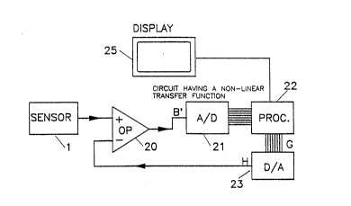
Fig. 8 shows an embodiment of a total system according to the
present invention. Analog image signals from the image sensor 1
are fed via a first input terminal into a device 20, which in
this embodiment is constituting an operational amplifier. An
output signal B' from the device 20 is further fed into an A/D
converter 21. The block 21 represent in principle, for example,
~ W093/239s2 ~1 3 ~ , 7 i PCT~SE93/00~4
any of the embodiments shown in Fig. 4 to Fig. 6. The output
signal from the block 21 in the form of a digital word, in the
demonstrated embodiment having 8 bits, is fed to a processor 22.
In the embodiment the processor is a personal computer provided
with a video monitor 25 on which the finally processed image is
presented. The processor precalculates and weights a correction
signal G which in digital form is fed to a D/A converter 23. In
the D/A converter the digital correction signal is converted into
an analog correction signal H, which is fed into a second input
terminal of the device 20 and which adds this to or alternatively
I subtracts this feedback signal H from the signal from the image
sensor~l dependent on which is applicable.
While the image sensor 1 is standing by it is, according to known
technique, continuously emptied of charges caused by the dark
current resulting in its different picture element first of all
due to the relatively high ambient temperature of the order 20 -
37-C. In the processor thereby is precalculated a measure of
this offset to which the device 20 should be set to compensate
this dark signal such that a totally unexposed picture element
should be exactly at the beginning of the signal level range
~marked by a in Fig. 2. By means of the multitude of picture
element in the image sensor an image ~s integrated during the
exposure of the image sensor by x-ray radiation simultaneously
as the processor 22 calculates a further supplementary correction
to the feedback signal H to the device 20 dependent of the
exposure time starting from the previous established dark current
correction, such that the least exposed picture elements will
subsequent be ~ust at the beginning of this interval a which is
having the steepest gradient in the relationship between signal
level and material density to thereby obtain the best posslble
gray level resolution in the weakest exposed portions which
princ1pally correspond to enamel and dentine in the image
obtalned in connection wlth the dental examination.
.
Finally in Fig. 9 is additionally shown another embodiment
according to the present invention. The embodiment of Fig. 9 is
:,
W093/23952 ~ 1 3 ~ S ~ i PCT/SE93/00404 ~ r ~:
$`~
demonstrating a solution utilizing the principal technique shown
in Figure 6, ~ut having the addition that the processor 22 like
the embodiment shown in Figure ~ calculates a correction which
is applied to the tabulated transfer function of the function
block 32. The A/D converter 31 utilizes in this embodiment like
in the block 5 of Figure 6 a greater number of bits than what is
finally applied to the processor 22. The tabulated corrected
transfer function is transmitted from the processor 22 to the
unit 32 which then preferably is constituting a RAM where the
output from the A/D converter performs the memory addressing for
the values to be read in the memory 32 and fed further to the
processor 22 in form of corrected values for the respective
picture element. The combination of memory 32 and processor 22
is additionally also possible to entirely be replaced by software
with a suitable processor 22.
In a further different embodiment of the present invention is
utilized a conventional linear A/D converter, eventually
integrated with the processor, instead of the unit 21 having the
non-linear transfer function, whereby the non-linear transfer
function is obtained by software for a fast processor 22
according to the method discussed previously in connection with
Figure 9.
In the embodiments digital words, e.g., having a resolution of
8 bits, have been utilized, but of course it is possible to use
any number of bits, anyhow preferably having a number being
divisible by four to, for example, utilize a number of words
having four bits. By such a higher contrast resolution having a
greater number of bits it is, for example, possible to also
present the image by means of pseudo colors, where different
color shades eventually more easily could indicate differences
in density than a pure gray scale on a display having a certain
limited light dynamics. By experience though it has been noted
that the black and white presentation so far has proven to be the
most effective way of presentation in this application of dental
x-ray images.