Note: Descriptions are shown in the official language in which they were submitted.
2134903
QUADRATURE SIGNALS FREQUENCY DOUBLER
Field of the Invention
This invention relates to a circuit for processing
quadrature signals and more particularly to a circuit,
preferrably an integrated circuit capable of processing a
pair of quadrature input signals so as to generate a pair of
quadrature output signals having a frequency that is double
the frequency of the input signals.
Backaround of the Invention
Quadrature signals, i.e. signals having the same
frequency but a phase difference of 90 (~/2), are used
with many circuits and find particular application in
circuits for fibre optic transmission systems and wireless
communications. One important property of quadrature
signals is that they can be multiplied to generate signals
having a frequency that is double the frequency of the
original signals. If the two quadrature signals are:
a = Asin(wt+ 0)
and
b = A cos(wt+ 0)
then by multiplying the two signals the result can be
written:
c = kA sin(2wt+ 0)
where k is the multiplier gain.
The quadrature signals frequency doubler circuit of the
present invention generates two quadrature output signal~
2134903
-
having a frequency equal to double the frequency of the two
quadrature input signals utilizing conventional integrated
circuit fabrication technology.
PRIOR ART
As discussed previously it is a property of quadrature
signals that they can be multiplied to generate quadrature
signals having double the frequency of the input signals.
In U.S. Patent 3,626,308, which issued December 7, 1971 to
T.O. Paine et al, a wide-band signal quadrature and second
harmonic generator is disclosed. A voltage-controlled phase
shifter is used to generate an output representing a phase
shifted sine input signal. A photoresistor is used to
control the output signal. The frequency range of this
circuit is limited to the range 100 Hz to 100 kHz and
includes components not compatible with integrated circuit
fabrication. U.S. Patent 3,676,660, which issued July 11,
1972 to L.R. Miller, relates to an analog computer and a
circuit that generates quadrature gating signals at both a
first frequency and a second frequency equal to twice the
first frequency. The circuit requires frequency doubler
stages, amplifiers and filters, i.e. the circuit is very
complex and not applicable to I.C. fabrication.
In the present invention a pair of dual phase shifters
is used to generate the phase difference between signals.
The use of phase shifters in related technology is known.
Eor example, P.A. Dawson and S.P. Rogerson in the IEEE
Journal of Lightwave Technology, Vol. LT-2, No. 6, pp. 926-
932, December 1984, describe a phase shifter circuit
consisting of two differential stages with connected
outputs. The input of the second stage is delayed by 0ma~
which delay is generated by an off-chip, fixed delay line
and accordingly a continuously variable frequency of
operation can not be achieved. H.M. Rein et al at the IEEE
International Solid-State Circuits Conference 1989 describe
in a paper entitled ~A 3Gb/s sipolar Phase Shifter and AGC
213~903
`
AmplifierN, a digital version of the circuit disclosed by
Dawson at al. This circuit according to Rein et al utilizes
a static master/slave flip-flop version of a frequency
divider for the generation of a phase difference. The
signal is halved prior to phase shifting followed by a
doubling stage to get the original frequency. A wide-band
low-pass filter is used to obtain continuous output signals
from the phase-shifting stage. This filtering stage
restricts the operable frequency range.
Summary of the Invention
It is an object of the present invention to provide a
circuit which is capable of generating, from a pair of
quadrature input signals of a first frequency, a pair of
quadrature output signals of a second frequency which
preferrably is double the first frequency.
It is a further object of the invention to provide a
circuit which can operate at any frequency from DC to the
maximum operating frequency allowed by the technology used
for implementation.
It is yet a further object of the invention to provide
n circuits which can be cascaded for a multiplication factor
of 2 .
Therefore in accordance with a first aspect of the
present invention there is provided a circuit adapted to
receive a pair of quadrature input signals of a first
frequency and to generate a pair of quadrature output
signals of a second frequency, the second frequency being
greater than the first. The circuit comprises a pair of
dual phase shifters each having input means to independently
receive the pair of input signals and to genereate a pair of
output signals having a phase difference therebetween.
Control means is connected to each of said pair of dual
phase shifters, the control means having phase adjusting
21~903
`
means to control the phase difference between the pair of
output signals. A pair of symmetrical multipliers are
provided, each of the pair receive the pair of output
signals from the phase shifters and generate a pair of
quadrature output signals having a second frequency which
according to a preferred embodiment is double the frequency
of the input signals. A biasing sub-circuit is provided
which supplies operating voltage to each element of the main
circuit.
According to a second aspect of the invention there is
provided a method of generating a pair of quadrature output
signals from a pair of quadrature input signals the output
signals having a frequency which is double the frequency of
the input signals. The method includes the steps of
supplying the pair of quadrature input signals to a pair of
dual phase shifters, each of the phase shifters having means
to generate a pair of phase shifted output signals. A
differential phase control signal is generated in a phase
controller and this signal is supplied to each of the dual
phase shifters to control the phase between the phase
shifted output signals. The phase shifted output signals
are supplied to a pair of symmetrical multipliers which
generate the pair of quadrature output signals having a
frequency which is double the frequency of the quadrature
input signals.
Brief Description of the Drawings
Figure 1 is a block diagram of the frequency doubler
circuit of the present invention;
Figure 2 is a schematic diagram of one of the dual
phase shifters;
Figure 3 is a schematic diagram of the dual phase
shifter controller andi
Figure 4 illustrates the phase relationship between the
quadrature input and output signals.
213~gO3
-
Detailed Description of the Invention
For identification purposes the quadrature input
signals will be identified as (hck,hckb) and (hckq,hckqb). The
quadrature output signals are identified as (ck,ckb) and
(ckq,ckqb). The phase difference between hck and hckq and
between ck and ckq is 90. All input and output signals are
of differential type.
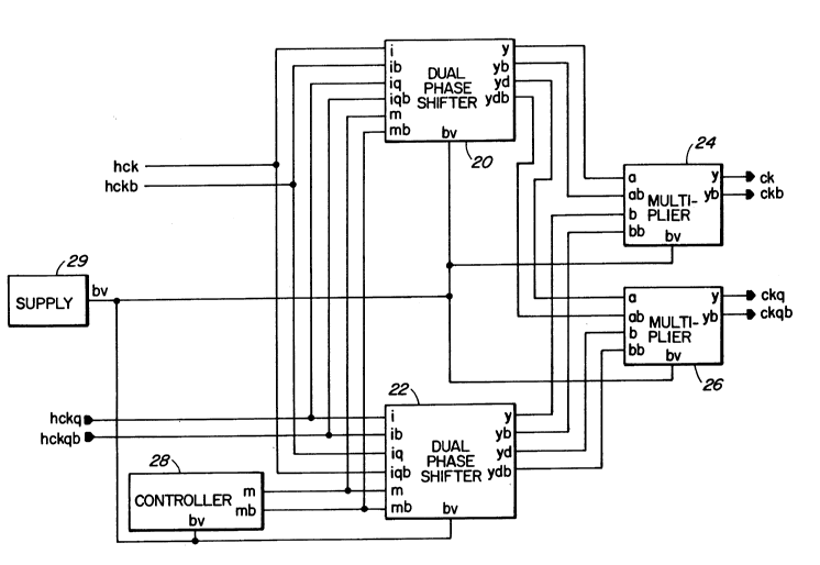
As shown in Figure 1 each of the pair of quadrature
input signals (hck,hckb) and (hckq,hckqb) is coupled to a pair of
dual phase shifters 20, 22. Respective outputs of each of
the pair of dual phase shifters are coupled to each of a
pair of symmetrical multipliers 24, 26. Dual phase shifter
controller 28 under control of bias voltage supplied by a
power supply 29 provides phase control to each of the phase
shifters 20, 22. Quadrature output signals (ck,ckb) and
(ckq,ckqb) as shown in Figure 1 are generated by multipliers
24, 26.
The dual phase shifter as seen in Figure 2 comprises
two multipliers each having their outputs connected as two
summing amplifiers. As shown in Figure 1 the quadrature
input signals are supplied to input terminals of the phase
shifters as follows:
input phase shifter 20 Dhase shifter 22
hck i iqb
hckb ib iq
hckq i iq
hckqb iqb ib
The outputs from each dual phase shifter are identified as
(y,yb) and (yd,ydb).
It is to be noted that the input signals are of
differential type for generality. If desired they can be
single ended in which case ib and iqb will be substituted
with reference voltages Vref and Vrefq respectively.
213~903
,
The manner in which these signal are processed in each
dual phase shifter will be described with reference to
Figure 2. As shown differential input signals (i,ib) are
supplied to the bases 44, 46 of transistors 40 and 42
respectively. Differential input signals (iq,iqb) are supplied
to the base 54, 56 of transistors 50, 52 respectively.
Current sources 48, 58 comprising transistor 47 and resistor
49 and transistor 57, resistor 59, respectively controlled
by bias voltage (bv) supply current to respective
transistors 40, 42 and 50, 52 via degeneration resistors 43,
45 and 53, 55 respectively.
The two current sources are shown for generality. They
can be replaced with resistors if desired.
- Emitter coupled second level transistors 60 and 70 are
connected to the collector 61 of transistor 40. Transistors
80 and 90, also emitter coupled, are connected to collector
81 of transistor 42. Similarly transistors 100 and 110 are
connected to transistor 50 while transistors 120 and 130 are
connected to transistor 52. Second level transistors 60,
70, 80, 90, 100, 110, 120 and 130 are controlled by
differential inputs (m,mb) supplied by dual phase shifter
controller 28 (Figures 1 and 3).
The operation of the dual phase shifter can be
described as follows:
differential input signal (i,ib) is defined as Asin(wt) and;
(iq,iqb) as Acos(wt) where;
(i,ib) and (iq,iqb) are the quadrature input signals and
A is the voltage amplitude of the input signals.
Then:
l I + Asin(wt)
213~903
`
where:
I42 = the collector current for transistor 42
I0 = the current supplied by the current source 48 as
controlled by DC bias voltage (bv). The total current
supplied is 21o;
Re = sum of resistors 43 and 45
also:
I _ I Asin(wt)
44 -- -- R
l44 iS the collector current for transistor 44. Other
values as set out above.
Acos(wt)
IQ = IO + Re
and
Acos(wt)
Iso = Io Re
where 15~ = collector current for transistor 52,
Iso = collector current for transistor 50,
I0 = current supplied by current source 58 (total
current is 2Io) and;
Re = sum of resistors 53 and 55.
The aforementioned collector currents are multiplied by m
and (1-m) respectively, where m < 1, by the upper
transistor pairs (60, 70), (80, 90), (100, 110) and (120,
130) under the DC voltage control (m,mb) as previously
discussed and supplied by dual phase shifter controller 28.
These multiplier circuits provide outputs (y,yb) and
213~903
(yd,ydb) via summing amplifiers comprising transistors 160,
162, 164 and 166 as well as resistors 170, 172, 174 and 176.
The summing amplifiers are shown for generality only.
The complementary output signals of each phase shifter
(y,yb) and (yd,ydb) can be approximated as:
(y,yb) = 2 R C [msin(wt)+(1-m)cos(wt)]
and;
(yd,ydb) = 2 RC[(l-m)sin(wt)+mcos(wt)]
where:
RC = load resistors (150, 152, 154 and 156).
The phase change introduced by the propagation time through
the phase shifter has been neglected in as much as only the
relative phase of the four output signals is of interest and
not the absolute value of the phases.
The two output signals can be rewritten as:
(y,yb) = Alsin(wt+ 0l) and;
(yd,ydb) = Alsin(wt+ 02)
where:
Al = 2 RC~(l-m)2+m2
l-m
01 = ~c~n
213490~
-
- and
02 = arCtall 1
The amplitude of the two output signals are the same,
and the relative phases are 01 and 02~ It is possible to
make 01 = 8 and:
02 - 8 by choosing an appropriate value of m.
The value of m is controlled by the phase shifter
controller best seen in Figure 3. The complementary outputs
m and mb are controlled by choosing the appropriate ratio
between resistor 140 and the sum of resistors 142 and 144.
This ratio can be chosen depending on the relative phase
difference desired. Control circuit 28 also includes
current sources comprising transistor 141, resistor 143 and
transistor 145, resistor 147. Transistors 146 and 148
provide outputs mb and m respectively.
From this analysis it is apparent that by utilizing the
circuit configutation shown in Figure 1 it is possible to
generate from two differential input signals having a
relative phase of ~/2, four output signals having relative
phases of 0, ~/4, ~/2, 3~/4.
Figure 4 is an illustration of the input signals and
their relative phases ( hck, hckb and hckq, hckqb) and the dual
phase shifter outputs and their relative phases. In Figure
4 the output signals of the two phase shifters 20 and 22 ( psl
and ps2) are identified as follows:
psl outputs y,yb and yd,ydb are psl.y, psl.yb, psl.yd and
psl.ydb
ps2 outputs y,yb and yd,ydb are ps2.y, ps2.yb, ps2.yd and
ps2.ydb
213~903
-
The output set of the four signals as shown in Figure 4
can be seen as a pair of quadrature signals having a
relative phase of ~/4:
- ( psl.y, psl.yb ) and ( ps2.y, ps2.yb )
- ( psl.yd, psl.ydb ) and ( ps2.yd, ps2.ydb )
By multiplying the quadrature signals employing the
circuit of Figure 1, a pair of output signals having a
frequency equal to double of the input signals can be
generated. The relative phase of the output signals is ~/2.
The multipliers are well known in the prior art and
will not be described in detail here. It is important,
however that multipliers be symmetrical in order not to
introduce phase errors.
As indicated previously the circuit can operate at any
frequency from DC to the maximum frequency allowed by the
technology used for implementation. An exclusive-or type
circuit can be used if a digital output signal is desired.
Another feature of the invention is that the basic
circuit as illustated in Figure 1 may be cascaded to double
the frequncy of the quadrature output signals. In the
cascade configuration the output shown as (ck,ckb) and (ckq,ckqb)
are supplied to a second similar circuit as inputs (hckl,hckbl)
and (hckql,hckqbl). Thus the multiplication factor for a
circuit having n stages is 2n.
While a specific embodiment of the invention has been
disclosed it will be apparent to one skilled in the art that
variations and alternatives to this embodiment can be
implemented. It is to be understood, however, that such
variations and alternatives will fall within the scope of
the invention as defined in the appended claims.
.