Note: Descriptions are shown in the official language in which they were submitted.
213~1SS
W O 93/2262Z P~T/U~93/04212
MONOLITHIC INTEGRATED CIRCUIT FOR USE WITHIN A ::
LINEAR YARIA~LE DIFFERENTIAL TRANSFORMER :
Cross-~eerence to Related AP~lications
This is a continuation-i~-paxt of pending
applicatio~ Serial ~o. 07~834,150 filed February 10,
1992, which is a di~ision of application Serial No.
07/483,657 filed F~bruary 23, 1~90, now U.S. Patent
No. 5,087,894, which is a division of application
Serial No. ~7/12~,118 filed No~ember 13, 1g87, now
U~S. Patent No. 4,904,921.
Field o the Invention
. This in~Qn~ion relates to interface circuitry ~.
for linear variable differential transormer
position transducers and, more particularly, to a
~onolithic i~tegrated circuit for driving the
primary winding of a linear variable differential :.
~ransormer and for decoding its secondary wi~ding
outputs to provide a highly a~curate analog vol~age
representatio~ of core position. The interface
~ircuitry is i~tended primarily for use with li~ear ~.:
~ari~ble differential transformers but is ~ot
limited to such use.
,~
~1~4'~ j
W093/22622 P~T/US93/o~
Backqround of the Inv ntion
T~e linear ~aria~le differential transformer
~L~DT) is a commonly-used linear position transducer
that includes a movable magne~ic core, a primary
winding and two secondary windings. Since there is
no contact between the core and the windings, there
is no friction and no mechanical wear to limit the
life o the ~ransducer. This is especially
important i~ high relia~ility applications and in
hostile environments. As an example, the control
surfaces of aircraft e~ibit vibra~ion which would
quickly destroy a mechani~al contact-type
transducer. The position of the magnetic core
determines the voltage induced on each of the two
secondary windings. When th~ core is approximately
centered in the secondary windings, an equal voltage
i,s induced o~ each secondary winding. As the core
is displaced from the center, or null point, the
voltage induced on one secondary winding incr~ases
while t~e voltage on the other secondary winding
decreases. The two secondary windings are usually
connec~ed in ~eries opposing, and the resulting
difference voltage is measured. The phase relati~e
to the primary voltage indicates th~ direction
rela~i~e to the null point. In this scheme, ~he
primary drive voltage is a scale factor that
directly affects the output Yoltage, and must be ~:
ætabilized. . :~
Another prior art detection scheme for LVDT's ~ .
employs synchronous full:wave detection. Since ~he
W093~22622 2 1 3 4 ~ ~ ~i PCT/USg3/042}~ -
output voltag~ goes to zero at ~he null point, the
reference signal for synchronous det~c~ion must be
dexived from the primary *ri~e-sig~ Since there
is usually a phase shift between the pri~ary and
s~condary signals, a ~omp~nsating phas~ shift must
b~ added to ~he r~ference signal. The required
phase shift complicates the det~tion ~echnigue, and
exrors are introduced if the phase ~hift is .
incorrectly compensa~ed. In this sch~me, the scale
factor is also sensitive to amplitude variations of
the primary drive signal.
In the past, the interface circuitry~for LVDT's
was mounted on pri~ted circuit boards a~d r~quired
various adjustments, thereby making LVDT's
relatively inconvenient to use as position
transducers. It is desirable to inaorporate the
drive and.deteation circui~ry for LVDT's in~o a
module or integrated aircuit that provides a vs~tage
represe~tative of core position. Such an in~egrated
circuit should be hiyhly accurate and should be
adaptable for use with a variety of different LVDT
types. In addition, it should have a minimum of
required e~ ernal components, particularly variable
components and active compo~ents, and should be easy
to use.
An integrated ~VDT interface circuit is ;:
described by ~icholas ~. ~ray in "Simplifying LVDT
Signal Conditioning," Machine_~e~gn, May 7, 19~7,
pp. 103-lO~ and by Zahid Rahim, "LVDT Interface
Chip's Fu~ctional Blocks O fer Versatility," EDN,
213~Q~
WO~3~22~22 PCT/US93/04212 ~
May 29, 1986, pp. 159-168. The interface circuit r
descrîbed in those references utilizes the
~traditional technique of synchronous de~F~i-o6. ~n
external voltage reference and an external
adjustment of the re~erence signal phase are
required. Since synchronous detection is u~ilized,
the above-described sensiti~ity to variatio~s in
primary dri~e ~oltage is present. In addition, a
change in phase shift from the-primary to the
secondary or an error in ~he phase s~ift network
represents a scale factor error.
An LVDT interface circuit having a binary ..
encoded output is described by Daniel Denaro in
"Transducer Converters Ease Industrial
Measurements," Electronic l~si~n, Septèmber 4, 1986,
pp. 118-124. The disclo~ed interface circuit
utilizes a ratiometric closed loop conversion
technique.~Another digital LYDT interface circuit
is:described in DD~ News, October 1987.
It is desirable to provide an LVDT interface
circuit that;is insensiti~e:to~primary voltage
~ariations, that has a scale factor and offset which
are relatively;insensiti~e to temperature ~ariations
and that has substantially better;linearity than the
LVDT transducer.; Furthermore, the~circuit must be
small in size, haYe a minimum of external components ~.
and be con~enient to use.
It~is a:general object~of the~presen~ in~ention
: to proyide a novel mo~olithic interface:circuit for
linear ~ariable differen~ial;transformer~s.
W093/22622 ~ 6 ~ PCT/U~93/04212
It is another object of the present invention to
provide an LVD~ interface circuit which generates an
analog output voltage that is a highly accurat~ ?
representation of core position.
It is yet ano~her object of the present
inven~ion to pruvide an r-VDT i~terface circuit
having a scale factor, whi~h rela~es output ~oltage
to LVDT core position, that i~ highly stable as a
~unction of ambient temperature.
It is still anothe~ object of ~h~ presen~
invention to provide an LVDT interface circuit that
has an ou~put voltage which is substantially
insensi~ive ~o varia~ions in the primary drîve
voltage.
Xt is a further object of ~he present invention
to provide an LVDT interface circuit wherein a
single passive compone~t determines the ~cale factor
which relates output ~oltage to LVDT core position.
It is a further object of the present invention
to provida an LV~ interface circuit tha~ has
substantially better transfer function linearity
than conventional LVDT interfa~e circuits.
It is a further object of th~ present in~ention
to provide an LVDT interface circuit that can
selectably generate an output which is thQ integral
of c~re po~ition for closed loop applications.
Xt i~ a furthe~ object of th~ prese~t inventi~n
to provide an LVDT int~rface circuit in which ~he
primary drive sig~al i~ ea~ily programmable in
amplitude and frequency.
2131~
W093/22622 PCT~US93/04212 ^
;:
.~ -6-
I~ is another object of the present invention to
pro~ide a monolithic integrated LVDT interface
circuit ~hat is compact and re~urres--d ~ im~m-of
external components.
I~ is another object of the present in~ention ~o
provide a decoder for processing a pair of signals
of Qqual frequen~y to determine the ratio of .
amplitudes.
...
Summary of the InYention
According to the present invention, these and
other objects and advantages are achieved~in a ::
decoder for processing a pair of signals of equal
freguency to determine their relati~e ampli~udes.
The decoder is typically used in a~ interface
circuit for a linear variable differential
transformer position transducer,:but is not limited l~;
to such use. The ~VDT includes a primary winding, ~
pair o secondary windings and a movable core. The j!:
decoder is responsive to signals induced in the
secondary windings of the LVDT for computi~g the `"
position of thQ~LVDT core.
In a first~embodiment of the invention, the :
decoder includes means for rectifying and fil~ering
a pair of signals to~p~ovide d~tected A and detected
B sig~als, a charge balanc~ loop responsive to the
deteated A and detected B signa1s~for~proyiding a
~inary signal having a duty cycle representative of ;
B/tA~B) (or A/(A~B) if the var:iables are defined
di~ferently),: whére A and B represent the respective ,~
W093/226~2 ~ 1 3 -~ :~ G S PcrJusg3/o42l~
amplitudes of the pair of signals, and output
circuit means responsive to the binary signal for
providing the ~alue of K(A-B)/(A+~), wher~ ~ is a
co~stant sQale ~actsr.
The charge balance loop in ~he first embodimen~
prefexably comprise~ first multiplier mea~s for
multiplying the de~ected A si~nal by the binary
signal and providing a first multiplier output,
second multiplier m~ans for multiplying the detected
B sig~al ~y the binary signal in~erted and pro~iding
a second multiplier output, integrator means
responsi~e to the first multiplier ou~put fQr
integrating in one direction and responsive to ~he
sec~nd multiplier output for integrating in the
opposite direction, and comparator means for
comparing the output of the integra~or means with a
predetermined reference signal and pro~iding ~he
binary signal.
The output circuit m~ans preferably compris~s
means for providing a reference curren~, third
multiplier means for multiplying ~he referen~e
current ~y the binary si~nal and providing a third
multiplier output, four~h multiplier means for
multiplying the ref~ren~e current by ~he binary
signal invert~d a~d providing a fourth multiplier
output, summing means for obtaining the dif~erence
between the third multiplier output and ~he fourth
m~ltiplier output, lowpass filter means for
filtering high frequency compone~ts of the
differe~ce output of the summing means ~nd
213'1~5
W0~3/22622 PCT/US93/0421' "
-8- :
operational amplifier means for converting tAe
filtered dif~erence output ~o an outpu~ voltage.
In a second embodime~t o~he invention,.the
decoder inaludes means for rectifying and filtering
a pair o~ ~ignals ~o provide detected A and detected
B signals, a charge balance loop responsive ~o the
detected A and detected B signals for providing a
binary signal having a duty cy~le representative of
(B-A)/2B, where A and B represent the respec~i~e ,~
amplitudes of ~he pair of sisnals r and output ~`
circuit means responsive to the binary signal for
providing ~he value of K A/B, where K is~a constant
saale f actor .
The charge balance loop in the second embodiment `~
preferably comprises first multiplier means for
multiplying the detected B sîgnal by the binary
signal and providing a first multiplier output,
second multiplier means for 1nultiplying the detected
B signal by the binary signal inverted and pro~iding ~`
a second multiplier output, integrator means
responsive to the detected A signal and to the first
mul~iplier output for i~tegrating in one direction
and responsive to the second mul~iplier outpu~ for
in~egrating in the opposite direction, and
comparator means for comparing the outpu~ of the
integrator means with a predetermined reference
level and providing the binary signal.
Brief DescriPtion of the Drawinqs
For a better understanding of the present
:i.
' .'
'.:;.
.... . . . . , : .. ...... .. ...... . . . .. ...... ..... . .. . . . ... . .. . ... ... .. .... . . . . . ... . ..
... . . . . . . . . . . . . .
W093/~622 2 ~ PCT/US93/04212
invention ~ogether with other and ~urther objects,
advantages and capabilities thereof, referen~e is
made to ~he accompanying drawin ~ ~ are.--
incorpora~ed ~erein by refere~ce and in which:
FIG. lA is a simplified block diagram of an ~VDT
syste~ in accordance with ~he pr~sent inYention;
FIG. lB is a graphic represen~ation o LVDT
secondary voltages as a function of core position;
FIG. 2 is an interconnection diagram for ~he
mo~olithic L~DT interface ~ircui~ in accordance with
~he present invention;
FIG. 3 is a fun~tional block diagram of the
decoder portion of the L~DT interfaca circuit;
FIGS. 4A-4D include a detailed schematic of the
decoder portion of the LVDT int0rface circuit;
FIG. 5 is a ~implified schematic diagram of ~he
output circuit of the decoder of FIGS. 3 and 4;
FIGS. 6A-6C include a detailed schematic diagram -
of the primary dri~er portion of the LVDT interface
circult;
FIG. 7 is a functional block diagram of an
alternate embodiment of a decoder;
FIG. 8 is a simplified block diagram of another
LVDT system in accordance with the present invention;
FIG. 9 is an int~rco~nection diagram for the
monoli~hic LVDT interface circuit of FIG. 8 in
accordance with the present invention;
FIG. lO is a ~unctional blo~k diagrzm of a
decoder that may be utilized in the system of FIGS.
8 and 9; -
W093/22622 2 1 3 ~ ~ 6 S PCT/US93/04212 ~
FIG. 11 is a simpliiëd schematic diagram of the
change balance loop in the decoder of FIG. 10; and
FIGS. 12A-12C are timing diagrams that . ~
illu~trate the i~tegrator voltage and comparator
output in the circuit of Fig. 11 ~or different input
conditio~s.
Detall-d nSO~ilLtion of the Invention
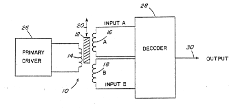
A block diagram of an LVDT system in accordance
with the present invention is shown in FIG. lA. ~n
LVDT 10 includes a movable core 12, a primary
winding 14 and a pair of secondary windings 16 and
18 designated as A and B, respectively. The LVDT
typically has the shape of a solenoid wi~h the core
12 linearly movable alo~g the axis in the dir~ction
indicated by the arrows 20 in FIG. lA. The primary
winding 14 is axially ce~tered in the devic~, a~d
secondary windings 16 and 18 are located an opposite
~nds of primary winding 14. Such de~ices are
well-~nown in the prior art and are commercially
a~ailable.
The secondary output ~oltages o~ the LVVT 10 as
a function of core 12 position are illustrated in
FIG. 1~. The primary winding 14 is dri~e.n by a si~e
wave, and the ou~put signals on seco~dary windings
16 and 18 are proportional to the displacement of
core 12. As the core 12 moves in a positi~e ! ~ ;
direction, the signal in secondary winding 16
de~reases as indicated by curve 22, and the signal
in secondary winding 18 increases as i~dicated by
W093/2262~ 2 1 ~ 5 PCT/US93/04212
1 1 !
curve 24. For core movement in a negative
direction, the winding 16 signal increases, and the
wi~ding lB signal decreases. When the core 12 is ;
centered, the outpu~ Yoltages are equal. Typ;cally, `;,
~he two secondary windi~gs 16 and 18 are connected
wi~h theix voltages opposing each other so that at
the center or null position, the sum of the output
signals is zero.
The LV~T interfaae circuit of the present
invention includes a primary driver 26 that supplies
a sine wave excitation signal to primary winding
14. As described hereinafter, the excitation si~nal
is programma~le in both frequency and amplitude so
that a ~ariety of different LVDT types can be
utilized with the cirauit. The LVDT interface
circuit further includes a decoder 28 that receives :~
the secondary voltages ~rom secondary windings 16 ``
and 18 and pro~ides a highly accurate analog output
signal on a line 30. As described hereinafter, the
decoder 28 does not reguire a phase shifted primary
refarence signal. Furthermore~ the dec~der 28
~alculates an output ~ue that is substantially
i~dependent of the primary dri~e amplitude, ~hereby
improving accuracy.
The LVDT circuit of the present i~vention is a
monolithic integrated circuit~ A typical
i~terconnection diagram is shown in FIG. 2. An -
integratedicircuit package 32 includes primary
driver 26 and decoder 28. Primary winding li is
coupled to pins 2 and 3 of package 32; one terminal
.
; :
:,
: .
213~5
WO 93/:2262~ PCI ~J593/0421 2 - `
--12--
of secondary winding 16 is coupled ~o pin 10; one
terminal o~ winding 18 is coupled to pin 11; and the
other terminals of windings 16 and ~~ar~-F~pled to `~
grou~d. Ei~her terminal of secondary windings 16,
18 can be connected to the i~terface circuit. Thi~
is an important advantage si~e the secondary
windings 16, 18 can't be connected incorrectly by
the user. ~ resistor 34 coupled between pins 4 and :~
5 det~rmines the amplitude of the primary dri~e
signal, and a capacitor 36 coupled betw0en pins 6 `
and 7 determines the freguency of the primary drive
signal. A capacitor 3~ coupled between pins 8 and 9
and a capacitor ~0 coupled between pin~ 1~ and 1
establish time constants of secondary signal
filkers. A capacitor 42 coupled between pins 14 and
15 es~ablishes a time constant of a duty cycle
signal ~ilter in the decoder as described
hereinaf~er. A resis~or 44 coupled between pins 15
and 16 establishes the scale factor between output ~:
~oltage and core 12 movement. The output siynal is
taken between pins 16 and 17. Positi~e and negative
supply ~oltages, typically 15 ~olts, are supplied to
pins 20 and 1, respecti~ely.
A block diagra~l of the decoder 28 is shown in
FIG. ~. The input signals, INPUT A and INPUT B, are
sine wa~es from the LVDT secondary windings 16 and
18, r~spectively. The INPUT A a~d INPUT B signals
may be shifted in phase relative to eac~ other,
depending on the type of L~DT and the core position,
by as mu~h as 10. The phase ca~ also ha~e a 180
213~S
W093t22622 PCT/US93/04212
-13
dQgree ambiguity depending on how the secondary
windings 1~, ~8 are con~ected to the interface
circuit. The INPUT A signal is supplle~-t~
voltag~-to-current converter 50 and to a comparator
52. The outputs of converter 50 and comparator 52
are supplied to;a multiplier 54. The ou~put o
multiplier 54 is coupled through a lowpa~s fil~er 56
to a du~y cycle multiplier ~8. Similarly, the INPUT
B ~ignal is supplied to a voltage-to-current
converter 60 and to a comparator 62, the outputs of
which are coupled to the inputs of a multiplier 64.
The output o~ multiplier 64 is coupled t~rough a;
lowpass filter 66 to a duty cycle multiplier 68. A
duty cycle binary signal d is suppli2d to the other
input of duty cycle multiplier 58, and a duty cycle
~inary signal l-d is supplied to the other input of
duty cycle multiplier 68. The outputs of
multipliers 58 and 68 are algebraially summed by an
adder 70 to pro~ide (A+B)d~B. The adder 70 output
is supplied to an integrator 72, and the integrator
output is supp}ied to a comparator 74. The output
o~ comparator 74 is the duty oycle bi~ary ~ignal d
and l-d which are connected ~ack as the inputs to
multipliers :58 and 68. (The binary signal d is the
logical complement or inversion of the binary signal
l-d .
In an alternative embodiment of the decoder,
duty cycle multipliers 58 and 68 ar~ replaced by
analog multipliers,: and comparator 74 is not used.
The signal d Is ~o long-r a binary signal, but is
~:'
: . ,;
213~"(;S
W093/22622 PCT/US93JO4212
.. ~ 1
~14-
now an ana1og signal. This variation of the decoder -
may find utility where speed is more impor~a~t than
accuracy,
The outputs o~ comparators 5~ and ~2 detect the
zero crossings of the respecti~e INPUT A and INPUT B ~:
æig~als and toggle the respective multipliers 54 and
64 operating on the sine wa~e input signals now
conver~ed to the current domain, multiplying by +~
to pro~ide full wave rectification at the outputs of
mul~ipliers 54 and 64. The full wave rectified
signals are lowpass filtered by filters 56 and 66 to
extrac~ a mean absolute de~iation measure of ~he
input signal amplitude.
The outputs of ~ilters 56 and 66 are then
processed in a charge balance loop comprising
multipliers ~8 and 68, adder 70, integrator 72 and
comparator 74. The multipliers 58 and 68 are
di~erential pair switches wi~h ~h0 control input :.
bei~g the binary signal of duty cycle d. When the :~
binary signal d is a square wave of 50% duty cycl0,
then d - O.5 and each multiplier 58,~68 scales its
signal input by O.5. This correspor.ds to the null `
point o~ the LVDT where the INPUT A and INPUT B
signals are equal. When the du~y cycle of ~he
binary signal is differen~ from 50%, then the A ~nd -
B channels are scaled by different amounts. The
Qutputæ of the~multipliers 58 and 68 are subtracted
by adder 70, and the differen~ is integrated by
integrator 72. ~he output of integrator 72 is :
compar~d with a refer~nce level by comparator 74, :~
wo 213`~G~
93/22622 ~ PCT/US93/0421~
--15--
and the binary output of the comparator is the duty
cycle control signal supplied back to multipliers 58
and 68.
The bi~ary signal has a duty cyele d which
coI1tinuously ~ari~s from zero to unity. By
in~arting the sense o the binary signal at the duty
cycle multipliers, the d and l-d signals are
pro~ided. Since the input to the in~egrator 7~ is
driven to zero, the output of comparator 74 has a
duty cycle d s B~A+B). Thus, ~he duty cycle d of
the binary signal provided by the charge balance
loop represents the relati~e amplitudes of the I~PUT
and INPUT B signals. The excellent linearity of
the charge balance loop is the direc~ result of the
inherent accuracy o~ the duty cycle multipliers 58
and 68. When the duty c~cle multipliers 58, 68 are
replaced by analog multipliers as described abo~e,
the linearity is degraded, but the inputs can chan~e
quickly and the output will accurately follow the:
difere~ce between A and B normalized to the sum of
their amplitudes, or (A~B)/~A~B).: Keeping the
finite gain of integrator 72 in the expression for
the loop output reveals
A-B - s(T+l)
OUT = G (l~
. i , ~ B - s~(T~
: G
: ~here G - d.c. gain, : :
,:
~:
~: :
.
213~J~S
W093/226~2 PCT~US93/04212 ~`
-16-
T = tim~ constan~ o~ integrator, and
s = complex frequen~y.
This result shows ~hat low in~egrator 72 gain can . ~:
cause o~fsets and scale factor errors which will
~cale with A~B. This means that if the primary
drive is not cons~ant with temperatur~ c~using A+B
to change a~d the int~grator 72 gain is low, then
o~fset and scale actor drifts can occur.
A parallel path is also driven by the binary
signal output o~ comparator 74. The binary signal
is supplied to a multiplier 80, and the binary
signal inverted is supplied ~o a multipl~er 82. The
other inputs ~o duty cycle multipliers 80 and 82 are
constant currents Ire~ derived from a bandgap
reference 84. The outputs of multipliexs 80 and 82
are subtracted by an adder 86. The output signal
from addQr 86 is a current express~d as
Iref(A-B)i(A~B~. The signal current from adder 86
is supplied through a lowpass filter 88 to an adder
90. The output of adder 90 ~s suppli~d through an
integrator 92 to the output. The output signal is
coupled through a voltage-to-current converter g~
back to addex 90. The output sig~al of the decoder :
~an be expressed as ~sCaleIref(
~RScale is the user-selectable resistor 44 ~hat
establishes the scale factor as descri~ed
herei~after. A referred-to-output (RT0) of~set 96
cbupled from the bandgap reference 84 ~o adder ~6
acilitate~ con~erting th~ bipolar output from the
~VD~ ~o a unipolar output. It may also be used to
W093/22622 ~ 9 6 ~ PCT/US93/04212
-17-
adjust zero.
A detailed schematic of the LVDT decoder 28 is
` shown in FIGS. ~A-4D. The elements shown in the
blocl~ diagram of FIG. 3 are enclosed by dashed
lines. The V-to-I con~rert~r 50 (~IGS. 4C and 4D)
includes transistors 102, 104, 106, 108 with PNP
current sources includi~g transistors 110, 112; NPN
current sources including transistors 114, 116; and
NPN current mirrors including tra~sistors 210-~20.
Similarly, V-to-I ~onver~er 60 (FIG~. 4C and 4D)
includes transistors 122, 124, 126, 128 wi~h P~P
curren.t sources ins:luding transistors l30~, 132; ~PN
current sources including transistors 134, 136; ana
~PN current mirrors including transistors 238-248.
Transistors 140-148 pro~ide appropriate bias
curren~ to the conveters 50 and 60. The scale
factor of converter 50 is established by resistor
103, and the scale factor of con~rerter 60 is
established by resistor 123. The INPUT P. signal is
supplied to the base of transistor 102, and the
INPUT B signal is supplied to the~ base of transistor
126. The configuration shown in FIGS. 4A and 4~ was
chosen to maximize input voltage swing~with low
supply voltages. Inputs can come within se~eral
~b~ of either supply, and the dif~erential output .-
curre~ts come from ~l?N sources at VMINUS. The input
de~rices ~are PNP tr~sistors 102, :106 for ~he P.
channel, and transistors 122, 126 for the B
channel. These de~ices operate as followers with a
bias of 10 mi~rozmps supplied by trans~istors 114,
.
:
,~.
,
2 1 3 ~
W093/22622 PCT/US93/04212-
-18-
11~, 13~, 136, respectively. Since the inputs
de~ices operate as followers, ther.e is no
nonlinear~ty to correct. The nonli~ear~ties are
primarily caused by the Early vol~age, a~d the
no~linearity is be~ter ~han 200 parts p~r million.
Th~ inpu~ de~i~es are PNP becaus~ their emitter-base
junctions are harder to destroy than that of ~PN
transistors.
The comparator 52 (FIG. 4C) includes transistors
150-164, and th~ ~omparator 62 (~IG. 4C) includes ~:
transistors 170-184. In comparator 52, the input
de~ices 150, 152 are PNP for robustness. ~The INPUT
A ~ignal is supplied to ~he base of ~ransistor 1$0.
The transistors 154 160 form a rege~erative la~ch.
Transistors 154 and 158 can share a poc~et in the
integrated cir~uit as can transistors 156 and 160,
thereby minimizi~g aapacitance at these switching
nodes. The comparator 62 has a similar stru~ture
with the INPUT B signal supplied to the base of
transistor 172. Resistor 186 coupled between the
collectors of transistors 150 and lS2 a~d resis~or
188 coupled be~ween the collectors of transistors
170 and 172 each pro~ide hysteresis and close the
positive feedback loop for regeneration.
In the multiplier 54 (FIG. 4C)~ differential
pair multipliers, includi~g differential pair ::
transistors 202, 204, and differential pair
ransis~ors 2~6, 208, perform the ~
muitiplication under control of the sutputs of
comparator 52. The A cur~e~t from con~erter 50 is
.. ... .... , . . . . , . . . ... . . . . ... ... ... . .. , ........ ,.. . ..... ~,.... ....... ..... ....... .
... . . ...
W093/22622 2 1 ~ ~ ~ 6 ~3 P ~/US93/04212
--19--
supplied to transistors 202 and 204 through
transistors 210, 212 and 214. The negative or
invertffd A current rom converter 50 is supplied
through transistors 216, 218 and 2~0 to transistors
206 and 208 of ~ul~iplier 54. Similarly, multiplier
64 (FIG. 4C) includes differen~ial pair multipliers
inclufding differential pair trfansistors 23Q, 232, :~
and diff~rential pair transistors 2~4, ~36 which
perform ~he +/-1 multiplication under control of
compara~or 62. The converter 60 supplies th~ B
current through trfansistors ~38, 240, 242 to
transistors 234, 236. :The negative or in~erted B -;
current from converter 60 is supplied through
transistors 244, ~46, 248 to transis~ors 230 fand 232. `
The recti~ied output signal from mul~iplier 54 `
is coupled from transistors 204~208 to filter 5~ .
(FIG. 4C) ~hrough resistors 250, 252 to ;
cascode~connected transistors 254, 256. External
filter capacitor 38 is coupl~d between resistors 250
and 252. Resistors 250 anf~ 252 decrease the
re~uired value of ~he external ~ilter capacitor 38. ,.
The circuit works well with a 0.1 micro~arad
capacitor 3f~ when the LVDT primary drive signal is ;
2.5 K~z. The filter 66 (~IG. 4C) for the B channel
has a similar stru~ture. The rectified output from
multiplier 64 is coupl~d from transistors 230-~36 :~
through resistors 260, 262 to cascode-connected ! `'.
trf~nsistors 264, 266, respeatiYely. External fil~er
capaaitor 40 is coupled between resistors 260 and
262. ~ ~ ?
f ~
2 ~ 6 5
W0~3/~62~ PCT/US93~4212 ~
., :
; -20-
The A channel duty cycle multiplier 58 (FIG. ~C)
includes dif~erential pair transistors 270, ~72 and
diferential pair transistors 274, 276. The outputs
from filter 56 are c~upled to the commun emitters of
each differential pair, and the duty cycle bin~ry
signals d and l-d are coupled to the bases of the
diferential pair transistors 270-276. For the
fraction of time that they are:~urned on,
transistors 272 and 274 couple ~he detected A --
channel signal ~o the integrator 72. When these
transistors a~e off, then ~ransis~ors 270 and 276
dump the A channel signal to ~he positi~e voltage
supply VPLUS. When the A channel signal i~
connected to the integrator 72, the B channel signal
is dumped to VPLUS and ~ice versa. The ~ channel
duty cycle multiplier 68 (FI~. 4C) has a structure
similar to multiplier 58 and includes differential
pair transistors 280, 282 and differential pair
transistors 284, 2~6. The outputs o ilter 66 are
coupled to the common emitters of each diferential
pair, and the duty cycle binary signals d and l-d
are aoupled to the bases of the ~ransistors
280-2~6. When they are turned on, transistors 230,
286 couple the detected B channel signal to
integrator 7~. When ~hese transistors are off,
transist~rs 282, 284 dump the B channel signal to
the posi~i~e ~oltage supply VPLUS.
The subtra~tion represented by adder 70 in FIG.
3 is implemented simply by connecting the ~utputs of
multipliers 58 an~i 6B o that the A signal cause~i
.
W~93J22622 2 1 3 ~ ~ 6 ~ Pcr/uss3/042l2
!
-21-
the integrator 72 ~FI~. 4~) to ramp up, while ~he B
signal causes the integrator 72 to ramp down. At
any giv~n time, each channel is multiplied by one or
zero, but averaged over time, the A channel is
multiplied by the fraction o~ time that transistors
272 and 27~ are tur~ed on, and the B channel signal
is multiplied by one minus this fraction. The
simplici~y and compactness of ~he multipliers 58, 68 ;`
is essential ~o conser~e die area on the monolithic
integrated circuit of the invention. The fraction
of time that each signal is either discarded or
c~upled to the summing node cons~itutes an analog
multiplication.
The outputs of multipliers 58 and 68 are coupled `.
directly to opposite sides of integrator capacitors
290, 292 in integrator 72. Of~se~ t~mperature
stability is preserved by constructing the 100
picofarad integrator capacitor as two symmetric . '`
halves in order to balance the parasitic bottom
late lea~age. Transistors 294 and 296:are current
sources for the integxator capaaitors 290,:292.
Opposite sides o~ the integrator capaaitors 290, 292 ~`
are coupled through follower transistors 298 and 300 ~ ~`
and through trarlsistors 302 ~and 304 to transis~ors
310, 312 which~ ~orm a post amplifier that increases
the d.c. gain of the integrator 72 and reduces the
errors indica~ed in equation;(l). It is d~sirable~
~or the post amplifier to have limi~ed bandwidth to
limit the osGillation fre ~ ency~of~the char~e
balance loop. The bandwidth is limited~by
` :~
`: .
:~ :
2 1 3 ~ 3
W093/22622 P~T/US93/04212
-22-
. ~ ' . `' ' .
capacitors 306, 308 ~`p~pled between the collectors
of transis~ors 302, 304. The freguency of the duty
cycl~ binary signal is about consta~t f~r ~ri-~s
input levels, but the ampli~ude o~ ~he integrator
triangle wave changes as larger input signals cause
faster ramp rates. The collectors of ~ransis~ors
310, 312 are coupled to comparator 7~ (FIG. 4A~.
The comparator 74 comprises a two-stage :~
regenerati~e latch for high gain and high speed. A
irst stage regenerati~e latch includes transistors
320, 322, 324, 3~6. A s~cond stage regenerati~e
latch inclu~es transis~ors 330, 332, 334, 336. The
outpu~ of the secon~ s~age is the duty cy&le binary
signal d and the duty cycl~ binary signal in~erted
l-d, which are coupled to transistors ~7Q-27~ and
280-286 in multipliers 58 and 68, thereby closing
the ~harge balance loop. The duty cycle binary
signal also drives the multipliers 80 and 82 ~FIG.
4D), which axe implemented as a single differential
pair including transistors 34a and 342.
The configuratio~ of the ou~put section ~FIG.
4B) i~ shown in sim~lified fosm i~ FIG. 5. The
requirements are to take the switched current from
transistors 340 and 342, to filter out the high
fxequency components of ~he duty cy~le binary signal
and to supply the result to the output with a
pro~ision for a user-selectable scale factor. The
èxternal output ~ilter capacitor 42 is coupl~d
betwe~n the collectors of transistors 340 and 342.
The collector of transistor 340 is coupled through a
:
W093/2~6~ 2 1 ~ 4 ~ 6 ~ PCT/US93/0421'
-~3-
resistor 344 to the i~verting input of an
operational ampli~ier 34~. ~ resistor 34~ is
coupled between the in~erting input and ~he output `~
of opera~ional amplifier 346. The noninYerting
input of amplifier 346 is coupled ~o grou~d, and the
output is coupled through a resistor 35Q to the :
collector o ~ransistor 342 and to the opposite side
of capacitor 42. The collector of ~ransistor 342 is
also coupled to the in~erting input of an
operational amplifier 3~2. The ext~rnal scale
fac~or resistor 44 is coupled between the inv~rting
input and the output of amplifier 3$2, and the
noninverting inpu~ of amplifier 352 is coupled ~o
ground. The ou~put of ~mplifier 352 constitutes the
voltage output of the decoder 28.
Amplifier 346 and resistors 348, 350 function as
a current mirror that ~qualizes the currents in
resistors 348 and 350. This can b~ s~en by
considering that the inputs ~o amplifiers 346 and
352 are maintai~ed a~ virtual ground, while the
output of amplifier 346 is coupled to both resistors
348 and 350. ~hus, r~sistors 348~and 350 have egual
voltages appli2d to them and their currents are
equal. ~he current mirror sees only the low
freguency signal representing mechanical movemen~ of
the cor0 12, while the high fre~uency duty cycle
binary si$nal current flows in a ~ight loop through
capacitor 42. The difference current i~ balanced at
the s~mming junction of output operational amplifier
352. Th~ feedback e~ement for amplifier 352 is
213~9~
W093/2~622 P~T/US93/0421~ ~
-24-
normally resistor 44 which programs the output
voltage soale factor per unit of core movemenk.
~l~ernatively, the feedback element can b~ ~
capacitor for signal integra~ion,`a useful feature
when the ~VDT is us~d in a closed loop configuration.
Si~ce the operatio~al ampliiers 346 and 35
have a ~ommon noninverting input, they can be merged
in a novel ampliier confi~uration. Refer~ing again
~o FIG. 4B, th~ node coupled to the base of
transistor 360 and labelled GND is the noninverting
input shared by both operational amplifier loops
shown in FIG. 5 and is also the signal co~mon. The
nodes labelled x, y and z in FIG. 4B ~orrespond to
the nodes la~elled x, y and z in FIG. 5. The merged
operational amplifiers in~lude transistors 370-402.
Transistors 3~0, 372, 374, 376 comprise ~he
amplifier 346. Transistors 38Q, 382, 384, 386, 38
comprise the amplifier 352. A third loop including
transistors 3S0, 390, 392, 394 a~d 3g6 sets the bias
for all three legs o the input. The output circuit
includ~s ~ransistors 388, 400 a~d 402. ~he extQrnal
resistor 44 (RScale) that ~stablishe~ the
user-selectable ~cal~ factor is coupled between the
output terminal and node æ of the amplifier~ Th~
output circuit was chosen for its ability ~o drive
heavy capaciti~e loads. Since th~ output circuit is
actually the loop integrator, a capacitive load on
~he output has the effect of gradually increasing
the loop compensation and the circuit will not
os~illate. The ~onlinearity of the current i~put to
.,
W093/22622 213~ J PCT/US93/~4212
-~5-
voltage output of the output circuit is abou~ two
parts per million.
The output circuit shown in FIG. 4B provi~~es
seYeral ad~antages. I~ co~erts a di~f~rential
current suppli~d rom transis~ors 340 a~d 342 i~to a
sî~gle-ended vol~age output. Although the refer~nce
input to the amplifier (noninverting inputs of
amplifiers 3~6 and 352 in FIG. S~ is coupled to "
ground in the present ~o~figuration, ~his node can
be coupled to any desired reference potential. The
scale factor b~tween the ou~put voltage and ~he ~'
diferential current input is established by a
single s~ale resistor cou~led between the output and
nod~ z. Thus, there is provided a ~hree-input ~`
amplifier useful ~or conYerting a differentiaI
current to an outpu~ voltage with the scale factor
being establishe~ by a single, user-selec~able
resistor.
The tail or emitter current of transistors 340, ~`
342 is a dire~t output scale factor and must be made
low drift. The bandgap referen~e ~olta~e is supplied
to the base of transistor 410 tFIG. 4D), which aa~s
as an emi~ter current source for ~ransistors 340 and
34~. The bandgap referenc~ ~oltage is also supplied .
t.o the bases of tra~sistors 412 a~d 414 (FI~. 4D~.
In ~he RTO offs~ 96, the collectors of tra~sistors
~12 and 414 are ccupled ~hrough tra~sistors ~
418, r~spectively, to the collectors of transis~ors
340, 342 in the ~uty cycle multiplier. The emi~ters
of transistors 412, 414 are coupled to resistors
2134~6~5
W093/2262~ PCT/US93/04212
. ~ -26-
420, 4~2, respectively. The ou~pu~ offset can be
ex~ernally programmed by a resistor (not shown)
connected between one of resistors 420, 422 and
VMINUS or unequal resistors connected between
resistors 420 and 422, respectively, and V~I~US.
A schematic of the bandgap reference 84 is shown
in FIG. 6~ and includes transistors ~30 44~. The
output BGOUT is a stable bandgap vol~age pius one
diode drop. The diode drop compensates for the base
to emitter junction of the current sources being
dri~en to provide temperature stable current sources.
A detailed schematic diagram of ~he primary
dri~er 26 is shown in FIGS. 6A and 6B and includes a
sine wave oscillator 500 and a power dri~er 502. In
the oscillator 500 (FIG. 6A), a multivibra~or
includes transistors 504, 506, s08, 510 with
transistors 512 and 5}3 funotioning as current
sources. The frequency is programmed by the
external capacitor 36 coupled between the emi~ters
of tranæistors 504 and 506. :The multi~ibrator
provides a triangular wa~re output which is buffered
through a cross-coupled dif~erential follower
including transistors 520, 522, 524,~526.
The differential follower~dri:ves a sine wave
shaper network including transistors 530, 532, 534,
536 and ~esistors 540, 542,~544~ 546. The emitter
of transistor 524: is coupled to the base of
transistor 530 and is coupled through rssistor 540
to the base of tra~sistor 53~. The emitter of
transistor 526~is: coupled to the base of transistor
~ ~ ,
:
:: : : '
.
:
W093/22622 2 1 3 ~ ~ 5 ~ PC~/US93/~421'
27- -
536 and is coupled through resistor S46 ~o the base
of transistor 534. The base of transistor 532 is
coupled through resistor 542 ~o the collector o~ .
transi~tor S14, and the base o~ transistor 534 is
aoupled through resistor 544 to ~he collector of ;~
transi~tor 514. The emitters of transistors 530, -
532, 534 and 536 are commonly coupled to the
collector of current source transistor 549. The
collectors of transistors 530 and 534 are coupled :~
toge~her and form one outpu~ of the sine wa~e `.
shaper; the collectors of transis~ors 532 and 536
are coupled together and form the other output of
the sine wave shaper. Transistor 514 functions as a :~
current source for the ~ine wave shaper. The sine
wave shaper configuration of FIG. 6A is advantageous ;
in that only one current source 514 is required. :;
The magnitude of the current ~upplied by transistor :;:
S14 can be varied in order to suppress harmonics in
the sine wa~e output of the shaper. The tail :-
curre~t of the ~i~e wave shaper is a 100 mi~roampere
temperature stable current from ~ransistor 549 a~d ,
the bandgap reference. .;
The amplitude and frequency of the sine wa~e ;'.
should be constant with temperature. The current
supplied by transistor 549 to the sine wa~e shaper
is temperature s~able. In order to provide a
temperature stable sine wa~e output, the scale
factor of the sine wave shaper and the peak-~to-peak :-
ampli~ude of the triangle wave supplied to the sine
wave shaper must both be proportional to absolute
:;
21~6~
W093/226~2 PCT/VS93/0421'
!
-28-
temperature. This proportionality is established ~y
diode ~31, resistor 537 and transistors 533 and
S35. ~s a-result, the ~urren~s-supplied by
tra~sistors 512, 513 and ~14 are all proportional to
absolute temperature~ The scale factor of the sine
wave shaper is established by the current from
transistor 514 and resistors 542, 5~4, 540, 546.
With this arrang~ment, ~he multi~ibrator fre~ue~cy
is constant wi~h tempera~ure, but i~s amplitude is -
propor~ional to absolute temperatureO Consequently,
~he sine wave ou~put of the shaper is
temperature-stable in both amplitude and frequency.
The sine wa~e output from the oscillator 500 is
a differential current co~nected ~o ~he emitters of
transistors 550, 552 in power dri~er 502 (FIG. 6C).
The driver circuit performs ~wo functions. It
centers the common mode of the diferential primary
drive half-way between VPLUS and YMINUS.
Transistors 554, 556 and resistors 558, 560, 562,
564 form V-to-I converters. The ~wo nodes mar~ed
LEV are utilized to program the primary signal
amplitude by shunting a portion o the signal~
Since ~ransistors 56~ and 568 pass equal currents,
the loop for es transistors 554 a~d 556 to have
.egual curren~s despite the imbala~ce introduced by
dif~erential sine wave input. Si~ce the V to-I
conver~er is driven to a null, there is
'nonlinearity ~o correct, and ~his section of ~he
circuit has a total harmonic distortion of 100 dB
down.
i'
~13~9~t)
WQ93/2~622 PCT/US93/~421~ `
-29-
The power output stages form th~ loop integrator
with the driver as an input transcondu~tance. The ~`
olltput load is directly con~ected to ~h~ loop
in~egxator in order tha~ large capacitive loads ca~
be driven. I~ is ~ecessary to drive ~he LVDT ;;
through a long cable if the application is i~ an ;~`
environment hostile to silicon ~ircuitry. ~nother
requirement is to current limit i~to an inductive ::
load. When current limit turns on, di/dt goes from
large to zero, causi~g ~he inductor ~ol~age to
collapse. When the core of an LVDT is removed, the ,;
primary inductance drops by about a facto~r of ten, :;:
and this is when the most severe overloads can be
expected. The dis~ortion of the amplifier is about
50 dB down when dri~ing 2S milliamps and increases .:
to lOO dB down with no load. The output stack for
one power amplifier compris~s tran~i~tors 570, ~72
and 574, while the output stack or the other power
amplifier ~omprises tranæistors ~76, 578, 580. :;
A thermal shutdo~ circuit for the primary
driver includes transistors 582, 584, 586, 588, 590
and 592. The the~mal shutdown circuit produces a
current which increases rapidly as a flmction of
~em?erature. The collector of transistor 584 is ;~
coupled to the collector of transistor 549, the
current sour~e for the sine wave shaper. When the :.
current ~hrough transistor 584 increases du~ to a
temperature ln~rease, the sine wa~e shaper emitter
current is reduced. As a result, output amplitude
of the sine wave shap~r decreases wit~out
.,
W093,2 21~4~GS
2622 PCT/US93/042t2
-30-
substantial harmonic.distortion. The thermal
shutdown circuit is designed to begin reducing the
current through the sine wave shaper at about 145C
and to gradually reduce the cur~ent to zero at about
165C. It will be understood that diferent
~emperature ranges ~an be sel cted for operation of
~he thermal æhu~d~wn circuit.
The gradual reduction in sine wave output
amplîtude as a unc~ion of temp~rature produced by
~he thermal shutdown circuit is particularly
advantageous in connection with the LVDT decoder
described hereinabove. The decoder is relatively
insensitive to primary drive sig~al variations since
it calculates the ratio (A-B)/(A~B). Therefore, as
the thermal shutdown circuit goes into operation and
reduces the sine wave amplitude, the decoder can
continue operation with high accuracy. At ~ery low
sine wave amplitudes, decoder errors w~ll increase.
However, until that point, accurate o~eration is
maintained even though the maximum ~emperature of
the drive circuit has been exceeded. The disclosed
thermal shutdown circuit, therefore, pro~ides a soft
or gradual thermal shutdown which may be
advantageouæ in cases of temporary high temperatures.
A monolithic integrated circuit incorporating `
~he circuitry of FIGS. 4A-4D and 6A-6C~has been
cons~ructed for operation with LVDT position :
transducer~ he integrated circuit needs no i ~ -
external active elements and no external
adjustments. ~Measured scale~actor stability is 20
..
.:
;...
,:
W093~2262~ 2 1 3 ~ ~ 5 ~ PCT/US93/04212
.
-31-
parts per millian per degree C. Offset stability is ~~.
10 parts per million per degree C and nonlineari~y
. is 0.0~. percent, ~ar better than that of a typical J,~''
LVDT. These results were achieved wi~hout '
trimming. With regard to the oscillator 500,
measured tempera~ure stability o~ the sine wave
amplitude is 1,000 parts per million per dPgree C,
frequency stability is 250 parts per million per
degree C and harmonic distortion is ~S dB dow~. The
in~egrated circuit described he~ei~ dramatically
reduaes the cost and complexity of using an ~VDT
position transducer, while pro~iding bett~r
performance. The circuit operates either on a
~ingle or a dual supply with total supply ~oltages
as low as 10.8 ~olts. The quiescent current is 1
milliamps. The inte~rated circuit is fabricated in
a junction-isolated bipolar process with 14 micron,
3 ohm-cm epl, SiCr thin film resistors, silicon
nitride capacitors and two level metal.
The LVDT interace circuit shown and described ~ :
hereinabove ls substantially insensitive to
variations in the primary drive ~oltage since it
calculates the ratio K(A-B)/(A~B). In addition, the
circuit described herein elimin~tes the requirement
~or phase shifting the primary drive:~oltage and
supplying it to the secondary decoder circuit,
thereby eliminating a source of potential errors.
~r~hermore,;the decoder 28 shown and described
herein is insensitive to phase shifts whi~h may
occur between the two secondary ~oltages of an LVDT.
:
:
21~9G~
Wos3/22~22 PCT/US93/04212
-32-
An alternate embodiment of the decoder is
simpler than ~he decoder of FIG. 3 and is useful in
~ituations where a phase shift between the A .and B
signals is not expected. ~n example of such a case
may be in decodi~g the ou~puts of a bridge circui~
The alternate embodiment is illustxated in block
diagram form in FIG. 7. Sine wa~e signals are
processed directly withou~ detection. ~ sîngle
comparator 602 sen~es the polarity of the A and B
input signals and then effe~ts a +/-l multiplication
just prior to i~tegration. The INPUT A signal i8
provided to a V-to-I converte~ 604, and the INPUT B
signal is supplied to a V-to-I converter 606. The
output o~ converter 604 is supplied to a duty cycle
multiplier 608, and the output of conver~er 606 is
suppli~d to a duty cycle multiplier 610. The ;
multipliers 608 and 610 recei~e duty cycle binary
si~nals d and l-d, respectively, rom the QUtpU~ 0~ ~:
a charge balance loop. The outputs of multipliers ~
608 and 610 are summed in an adder 612, and the ::
adder QUtpUt 612 iS supplîed to a multiplier Sl4.
The control input of multiplier 6i4 is the binary
output of comparator 6~2. The output of multiplier
614 is supplied to an integrator 616, the ou~pu~ of
which is sensed by a comparator 61~8~ The output of :.
comparator 618 is the duty cycle binary signals d
and l-d whiah are ~oupled to multipliers 608 and
610, respectively. The comparator 618 output is
a~lso supplied through an output circuit 62D which .
may be co~structe~ as described~hereinabo~e in
;, .~
~: -
.
~: ..
,
.:
: : :
213g9~S ':
W093/Z2622 PCT/US93/04212
-33-
connection with FIGS. 3 and 4A-4D. As noted above,
the circuit o~ FIG. 7 operates satisfac~orily when
the INPUT A and INPUT B-signals are in phase.
Howe~er, when these signals are phase shifted, the
output is erraneous during ~he time between the zero
crossings of the two si~nals. `
I~terface circuitry that is particularly useful
for a five-wirP LVDT system as shown in FIGS. lA and
2 has been described above. This circuitry can be
adapted for a four-wire LVDT or half bridge type
position transducer. Such transducers are similar ;~`
to those described above in that they have two
windings around a movable core and produce outpu~ :
signals propor~ional to the core position. A block
diagram of a four-wire LVDT system in accordance
with the present inv~ntion is shown in FIG. 8. An
~VDT 710 includes a movable core 712, a p~imary
winding 714 and a pair of seco~dary windings 716 a~d
718. The ~VDT typically has the shape of a
s~lenoid, with the co~e 712 lin~arly movable along
the axis in the direction i~dicated by the arrows
720 in FIG. 8. The primary winding 714 is axially
centered in the device, and secondary windings 716
and 718 are located on opposite ends of primary ::
win~ing 714. A primary driver 726 is coDnected to
primary wi~ding 714. Unli~e FIG. lA, the two
secondary wi~d~.ngs 716 and 718 i~ FIG. 8 are
connected series opposing so the output is a
diff~rence signal which ~aries li~early with core
712 po~ition.~ In FIG 8, secondary windings 716 and
.
: :
~` :
W093/226222~
PCT/US93/04212
3~
., ~, .
718 are connected to a channel A of a decoder 728,
and primary winding 714 is connected to a channel B
of decoder 728. Decoder 728 receives inputs A~
ACoMp and BIN, and computes the ratio A/B. The
circuit shown in FIG. 8 is insensitive to the
am~litude of the primary drive but is sensiti~e ~o
phase shif~s. : .
One probIem that has been ~ncountered with thi~
type of ~VDT system~is that when the core 712 is
centered, the output ~ignal amplitude is too small
to trigger the input comparator o~ the full wave :~
rectifier in the decoder of FIG.: 10. One way to
avoid this problem is to use the primary driver 726
to trigger the A ahannel comparator:752 in the
decoder 728 as discussed below. This allows the use
of the entire stroke of LVDT core 712, includiny the
~passing through~the center:position. ~he phase
~hift between primary winding 714;~and:;secondary
windings 716:and 718 is addressed~by introducing a
phase delay 722 between input signals BIN and
ACoMp. This,~hase:delay 722 is external and is ~ i!
adjustable with a trim~potentiome~er:::724. :
As with the LVDT circuit of~FIGS~ 7, the LVDT
circuit of FIG.~8~can be:realiz~ed as a monolithic
integrated circuit.;~An inter:connection diagram for ~ : :
such an integrated circuit is~:shown in FIG. 9. An
integrated circuit package 732 includeslprimary
dri~er 726 and~decoder:728. Primary winding 714 is
coupled~to pins~2 and 3 of package 732; one terminal
of seconda:ry~winding~:716 is~coupled~to pin 12; and
e termin-l of -econdary v:ndlng 718~is coupled:~o ;:
WO 93/2~622 ~ 1 3 4 9 G .~ Pcr~us93/o42
--35--
pin 13. The primary drive amplitude is set by a
resistor 734, and the primary drive frequency i~ SPt
by a capacitor 73~ capacitor 738 coupled between
pins 8 and 9 and a capacitor 740 coupled be~ween
pins 16 arld 17 establish time constants of secondary
signal filters. A capacitor 742 coupled b~tween
pins 18 and 19 establiæhes a time co~stant of a duty
cycle ~i~al filter in the de~oder 728, similar ~o
capaci~or 42 shown in FIG. 2 and described above. A
resistor 744 coupled between pins 19 and 20
~stablishes ~he s~ale factor b~tween output ~oltage
and ~ore 712 movemer~t. The output signal is taken
from pin 20. Positive and rlegati~re supply voltages,
typically lS ~rolts, are supplied to pins 24 and 1,
respectively.
A block diagram of decoder 728 is shown in FIG.
10. The input signal AIN is supplied ~o a
voltage-to-surrent co~erter 750, and input signal
ACoMp is supplied to a comparator 752. The :
outputs of converter 750 and comparator 7S2 are
~upplied to a multiplier 754. The output of
multip}ier 754 is coupled through a lowpass filter -~
75~ to an adder 770. Input signal BI~ is supplied
: to a ~oltage-to-current converter 7i50 and to a
comparator 762, the ou~puts o which are coupled to
the inputs of a multiplier 764. The output of
multiplier 764 i8 c:oupled through a l~owpass f ilter
766 to duty cy~le multipliers 758 and 768. A duty
cycle binary signal d is supplied to the other i~spu~
of duty cycl- multiplier 758, a~d a duty cycle
2 134~6S
W093/22~2 PCT~US93/04212
-36-
bi~ary signal l-d is supplied to ~he other input of
duty cycle multiplier 768. The respective outputs
of filter 756, duty cycl2 multiplier;758 and duty
cycle multiplier 768 are algebraically sum~ed by
adder 770 to proYide A ~ d)B ~ dB~ The adder 770 ;~
output is pro~ided to an integra~or ?72, and the
integrator output is supplied to a comparator ~74.
~he outputs of comparator 774 are ~he duty cycle
binary signals d and l-d which are eonnected back as
the inputs to multiplier~ 758 and 768,
respectively. :The binary signal d is the logical
compleme~t, or inversion, o the binary signal l-d.
I~ an alternati~e embodiment of decod~r 728,
duty cycle multipliérs 758 and 768 are replaced by . ;.
analog multipliers, and comparator 774: is not used.
The duty cycle d is no longer ~inary, but is now an
analog signal. This ~ariation of decoder 728 may
fi~d u~ility where speed is more important than `.
ac~uracy.
The outputs of comparators 752 and 762 detect
the zero crossings of the respecti~e Aco~p and
BIN signals and toggle the respective multipliers :
754 and 764 operati~g on the sine wave input signals~
now converted to the current domain,~multiplying by
~l or -l to~provide ~ull waYe~rectification at th~ ~ ~
outputs of multipliers 754 and 764.::The full wave i;;
xectii~d ~ignals are lowpass filtered by filters
756 andi756 ~o~extract a mean absolute deviation
measur~ of the:inpu~ sig~al amplitude.
As~discussed~:abo~e, decoder 728~produces the ~ :
,!,
,` : ` :: ~`~
:: ~ ` :, : : '`
~, . . i~ ,. ,.,. ' ' ' `
~134~S
WO g3/22622 PCr/USg3tO421
-37-
signal A/B. In FIG. 10, the B signal is multiplied
by the duty cycle and by the complement of th~ duty .
cycle, and the difference be~ween the ~wo products
is then taken. This difference is summed with the A
signal and then integrated. The rest of FIG. 10 is
similar in construction and operatîon ~o the de~oder
o~ FI~. 3 described above. Since the input to ~he
integrator is driven to zero, the duty cycle, d, is
forced to equal ~B-A)/2B. The comparator 774 output
is supplied to an output ~ircuit 776 w~ich -
corresponds to the output circuit of FIG. 3,
including elements 80, 82, 84, 86, 88, 90~, 92, 94
and 96. The output of circui~ 776 is 1-2d which is
e~ual to A/B.
The outputs of filters 756 and 766 are processed
in a charge balance loop comprising multipliers 758
and 768, adder 770, integrator 77~ a~d comparator
774. The multipliers 758 and 768 are differential
pair switches with the control input being ~he
binary signal of duty cycle d. When the binary
signal d is a sguare wave of 50% duty cycle, then d
a O-S and each multiplier 758, 768 scales its signal
input by 0.5. This ~orresponds to the center point
of the LVDT where signal AIN is zero. When the
duty cycle of the binary signal is differen~ from
50~, then th~ d and l-d scalings are different. The
ou~puts o multipliers 758 and 768 are subtracted,
~nd ~he output of ilter 756 is added thereto, by
adder 770, a~d the resulting sum is integrated by
i~tegrator 772. The Qutput of integrator 772 is
213~
W093/22622 PCT/US93/0~21~ :
,
-38-
compared with a refere~ce level by comparator 774, ~ ~:
an~ the binary output~of the comparator is the duty
cycle control signal supplied back to multipliers
758 and 768.
The binary signal has a duty cycle d which
co~tinuously ~aries from zero ~o u~ity. By
inverting ~he sense o~ the binary signal at the du~y .
cycle multipliers, the d and l-d signals are :
provided. Since the input to the i~tegrator 772 is r~
driven to zero, the output of comparator 774 has a
duty cycle d = (B-A)J2B. Thus, the duty cycle d of
the binary signal pro~ided by the charge~balance
loop represents the relative amplitudes of the AIN
and BIN signals- : .
A block diagram representing the charge balance
:laop of FIG. lO is shown in FI~. ll. The integrator
772 is represe~ted by resis~ors 780 and 782 and ;.
capacitor 784. The A channel is represented by
current source 785 and lines 786 and 788, and the B
channel is represented by current source 789 and
switahes 790 and 792, alI of ~hi~h supply charging
aurrent to capacitor 784. The~state of switches 790
and 792 is controlled by the;output of comparator
774. In the~A channel, current is always supplied
through capa~itor 784. In the~B channel, the d :
aontroll~d current ~s:~dlivered to`the~:capacitor 78
with the opposite~polarity of~the l-d controlled
The :wavef~rms in FIGS. 12A-lX~ illustrate the
operation of the: charge bala~e~ loop. In FIGS.
w093/2262~ 21~ 65 PCT/US93/0~212
-39~
12A-12C.the triangular waves 794, 796 and 798
represen~ the ~oltage across capacitor 784, and ~he
binar~ signals 795, 797 and 799 represent the output
of comparator 77~. The waveforms for A = zero are
shown in FIG. 12A. When A = zero, the triangular
wave 794 is syrnmetrical be~ause only B current f lows
in and out of s::apacitor 784. When A is different
from zero, as shown in FIGS. 12B and 12C:, the
capacitor 784 slews up and down at different ra~es
and the duty cycle i5 modulated. The magnitude of
the A input current must be less than the magnitude
of the B input current for this circuit to work.
Waveform 7~6 i~ FIG. 12B illustrates the voltage
across capacitor 78~ when A is greater than zero.
Wa~eform 798 in FIG. 12C indicates the voltage
across capacitor 784 when A ~s less than zero.
The decoder shown in FIG. 10 can be implemented ;~
as a minor ~odification to the circuit shown in
FIGS. 4A 4D. In particular, with reference to FIG.
4C, the collectors of tra~sistors Q239, Q~42, Q24~,
and Q~45 are di~connected from the supply voltage
VPLUS. The collectors of transistors Q239 and Q244
are connected to the ~ollec~or of transistor Q206
~FIG. 4A). The collectors of transistors Q242 and
Q245 are connected to the collector transistor Q~07
(FIG. 4A). The collectors of ~ransistors Q240 and
; I Q246 remain c~nnected to the collector of transistor
Q207, and the collectors of transistors Q241 and
Q2~3 remain connected to the callector of transistor
Q206. In addition, the qalues of resistors R206 and
,
W093/~26~2 213 ~ PCT/US93/04212
-40-
R207 (FIG. 4A) are changed from 30K ohms to 15K ohms.
Whîle there have been shown and described w~at
are at present considered~the preferred embodiments
of the present inven~ion, it will be obvious to
those skilled in the art that ~arious changes and
modifications may be made therein without departing
from the scope of ~he invention as defined by the
appended claims r ~".
. ~
: '
``'
'''