Note: Descriptions are shown in the official language in which they were submitted.
21351~3
SPECIFICATION
Title of the Invention
FILM DEPOSITING APPARATUS AND PROCESS FOR
PREPARING LAYERED STRUCTURE INCLUDING
OXIDE SUPERCONDUCTOR THIN FILM
Background of the Invention
Field of the invention
The present invention relates to a film depositing apparatus and a
process for preparing a layered structure including an oxide
superconductor thin film, and more specifically to an improved film
depositing apparatus particularly for preparing a layered structure
including an oxide superconductor thin film and a dielectric thin film
and/or an insulator thin film, which has a clear interface with negligible
interface states, high crystallinity and excellent properties.
Description of related art
Oxide superconductors have been found to have higher critical
2 0 temperatures than those of metal superconductors, and therefore
considered to have good possibility of practical application. For example,
Y-Ba-Cu-O type oxide superconductor has a critical temperature higher
than 80 K and it is reported that Bi-Sr-Ca-Cu-O type oxide
superconductor and Tl-Ba-Ca-Cu-O type oxide superconductor have
2 5 critical temperatures higher than 100 K.
In case of applying the oxide superconductor to superconducting
electronics including superconducting devices and superconducting
213S125
integrated circuits, the oxide superconductor has to be used in the form of
a thin film having a thickness of a few nanometers to some hundreds
micrometers. It is considered to be preferable to utilize various
deposition methods, such as sputtering methods, laser ablation methods
5 and reactive co-evaporation methods for forming oxide superconductor
thin films. In particular, it is possible to deposit an oxide superconductor
thin film atomic layer by atomic layer through utilizing a reactive
co-evaporation method. Additionally, in-situ observation during and
between depositing thin film is possible so that a high quality oxide
10 superconductor thin film can be obtained by the reactive co-evaporation
method.
In order to deposit an oxide superconductor thin film on a substrate
by the reactive co-evaporation method, constituent elements of the oxide
superconductor excluding oxygen are supplied as molecular beams
15 towards the substrate by using Knudsen's cell (abbreviated to K cell
hereinafter) type molecular beam sources. In addition, an oxidizing gas
such as 2 including O3, NO2 or N2O is supplied near the substrate so that
the molecular beams are oxidized so as to form the oxide superconductor
thin film on the substrate. It is also possible to deposit high quality thin
20 films of ferroelectrics such as SrTiO3 and of nonsuperconducting oxide
such as PrlBa2Cu3O7 y. Furthermore, by switching molecular beam
sources, it is possible to deposit thin films of different materials or
compositions successively so as to form a layered structure.
In Canadian Patent Application No. 2,084,964-9, Takao Nakamura
25 discloses a film deposition apparatus suitable for depositing oxide thin
films by the reactive co-evaporation method. This film deposition
apparatus includes a vacuum chamber provided with a main evacuating
213~12~
apparatus, at least one K cell or at least one electron beam gun provided at
a bottom of the vacuum chamber, and a sample holder provided at a top
of the vacuum chamber for holding a substrate on which a film is to be
deposited. The sample holder is associated with a heater for heating the
5 substrate. In addition, the vacuum chamber is also provided with a liquid
nitrogen shroud for forming a cold trap around an evaporation source of
the K cell or electron beam gun, and a RHEED (Reflecting High Energy
Electron Diffraction) device for evaluating a depositing thin film. In
front of the substrate attached to the sample holder, a shutter is located
10 for controlling a deposition time during the deposition process. The K
cell and the electron beam gun are also provided with an operatable
shutter.
In addition, a gas supplying apparatus is provided so as to introduce
an oxidizing gas such as 2, 03, NO2, N20, etc. in vicinity of the substrate
15 attached to the sample holder, so that the oxidizing gas can be supplied to
form an oxygen-enriched atmosphere in the vicinity of the substrate in
order to oxidize molecular beams incoming from the molecular beam
source in the course of the film deposition.
Furthermore, the film deposition apparatus additionally includes a
2 0 partitioning plate for dividing the vacuum chamber into a first
sub-chamber which is constituted of a lower portion of the vacuum
chamber defined below the partitioning plate and which is coupled to the
K cell, the electron beam gun and the main evacuating apparatus, and a
second sub-chamber which is constituted of an upper portion of the
2 5 vacuum chamber defined above the partitioning plate and in which sample
holder is located. The partitioning plate includes a through opening
formed at a center thereof. The position of the opening is determined to
213~12~
ensure that a beam emitted from K cell and the electron beam gun toward
the substrate is not obstructed by the partitioning plate. In addition, the
size of the opening is determined to enable restricted molecular flows,
particularly of oxygen gas, from the second sub-chamber to the first sub-
5 chamber so that a pressure difference can be created between the firstsub-chamber and the second sub-chamber even if the opening is open.
Therefore, the partitioning plate having the through opening constitutes a
vacuum conductance.
A gate valve is provided on the partitioning plate for hermetically
10 closing the opening of the partitioning plate, so as to completely shut off
the molecular flows between the first sub-chamber and the second
sub-chamber when the gate valve is closed. An opening and closing of
this gate valve is controlled from the outside of the film deposition
apparatus.
In addition, an auxiliary evacuating apparatus is attached to the
second sub-chamber for evacuating the second sub-chamber to an
ultra-high vacuum even if the gate valve is closed.
By using the above conventional film deposition apparatus, a high
quality single oxide thin film of high crystallinity with excellent
20 properties can be deposited. However, it is difficult to form a layered
structure composed of a sharp and clean interface and thin films of
different materials or compositions with excellent properties.
In the above film deposition apparatus, a composition of a deposited
thin film is controlled by ratios of intensity of the molecular beams and
25 the intensity of the molecular beams is controlled by temperatures of
crucibles of the K cell type molecular beam sources. Therefore, accurate
- 213512~
temperature controls of the crucibles are required when the or molecular
beam sources are switched so as to deposit a different thin film.
Amounts of materials left in the crucibles and atmosphere around
the molecular beam sources effects on the intensity of the molecular
S beams and temperature distributions of around the out lets of the crucibles
are influenced by an operation of shutters. Therefore, the temperatures
of the crucibles should be stabled before starting the deposition of a thin
film. It takes long time to stabilize the temperatures of the crucibles so
that process for forming a layered structure is interrupted when the
1 0 molecular beam sources are switched so as to deposit a different thin film.
During the interruption, a lower thin film just deposited is
maintained at the depositing temperature so that contaminants in the
chamber may stick to a surface of the lower thin film or oxygen within
the lower thin film may escape so as to diffuse into the chamber of ultra
1 5 high vacuum.
In order to prevent the above phenomenon, it is proposed to stop
heating the substrate during the interruption so as to lower the
temperature of a lower thin film. However, in this case, a lower thin film
is repeatedly heated and cooled so as to subject large thermal hysteresis
2 0 which causes distortions and clacks of the thin film.
Summ~ry of the Invention
Accordingly, it is an object of the present invention to provide a
film depositing apparatus, which has overcome the above mentioned
2 5 defects of the conventional ones.
Another object of the present invention to provide a process for
preparing a layered structure including an oxide superconductor thin film
213~125
which has a clean and sharp interface, high crystallinity and excellent
properties.
The above and other objects of the present invention are achieved in
accordance with the present invention by a film deposition apparatus
5 comprislng:
a vacuum chamber provided with a partitioning means for dividing
said vacuum chamber into a first sub-chamber and a second sub-chamber,
said partitioning means including an opening for introducing a vacuum
conductance for molecular flows between said first sub-chamber and said
10 second sub-chamber so that a pressure difference can be created between
said first sub-chamber and said second sub-chamber even when said
OpeIling lS open;
a gate valve provided on said partitioning means for hermetically
closing said opening of said partitioning means so as to shut off the
15 molecular flows between said first sub-chamber and said second
sub-chamber;
at least two evaporation source sets each comprising at least one K
cell provided in said vacuum chamber in communication with an internal
space of said vacuum chamber and designed to deposit a thin film at
2 0 different deposition positions in said second sub-chamber;
a main evacuating means coupled to said first sub-chamber for
evacuating said first sub-chamber to an ultra high vacuum;
a rotatable sample holder located within said second sub-chamber
having at least two heads for holding substrate to be deposited so as to
2 S face different directions, said sample holder is rotatable so that said heads
can be located at said different deposition positions;
means for heating said substrates;
21351~5
a gas supplying means provided in said second sub-chamber so as to
supply a predetermined gas to said second sub-chamber; and
an auxiliary evacuating means coupled to said second sub-chamber
for evacuating said second sub-chamber to an ultra-high vacuum even
when said gate valve is closed.
In the apparatus in accordance with the present invention, all the
molecular beam source sets can be provided in the first sub-chamber in
communication with an internal space of the first sub-chamber.
According to another aspect of the present invention, there is
provided a film deposition apparatus comprising:
a vacuum chamber provided with at least two deposition rooms
arranged symmetrically and separated by a bulkhead;
each of said deposition rooms comprising:
a partitioning means for dividing said deposition room into a
first sub-chamber and a second sub-chamber, said partitioning means
including an opening for introducing a vacuum conductance for molecular
flows between said first sub-chamber and said second sub-chamber so that
a pressure difference can be created between said first sub-chamber and
said second sub-chamber even when said opening is open;
2 0 a gate valve provided on said partitioning means for
hermetically closing said opening of said partitioning means so as to shut
off the molecular flows between said first sub-chamber and said second
sub-chamber;
at least one evaporation source sets each comprising at least
2 5 one K cell provided in said first sub-chamber in communication with an
internal space of said first sub-chamber;
213~125
a main evacuating means coupled to said first sub-chamber
for evacuating said first sub-chamber to an ultra high vacuum;
a gas supplying means provided in said second sub-chamber
so as to supply a predetermined gas to said second sub-chamber; and
an auxiliary evacuating means coupled to said second
sub-chamber for evacuating said second sub-chamber to an ultra-high
vacuum even when said gate valve is closed;
a rotatable sample holder located within said vacuum chamber
having at least two heads for holding substrate to be deposited so as to
face different directions, said sample holder is rotatable so that said heads
can be located at deposition positions in second sub-chambers of the
deposition rooms; and
means for heating said substrates.
In a preferred embodiment, the oxide superconductor is formed of
a high-TC (high critical temperature) oxide superconductor, particularly,
formed of a high-TC copper-oxide type compound oxide superconductor
for example a Y-Ba-Cu-O type compound oxide superconductor material,
a Bi-Sr-Ca-Cu-O type compound oxide superconductor material, and a
Tl-Ba-Ca-Cu-O type compound oxide superconductor material.
2 0 In addition, the substrate can be formed of an insulating substrate,
preferably an oxide single crystalline substrate such as MgO, SrTiO3,
CdNdA104, etc. These substrate materials are very effective in forming
or growing a crystalline film having a high degree of crystallinity. Some
other substrates with above insulating buffers are also applicable.
2 5 The above and other objects, features and advantages of the present
invention will be apparent from the following description of preferred
~13512~
-
embodiments of the invention with reference to the accompanying
drawings.
Brief Description of the Drawings
Figure 1 is a diagr~mm~tic sectional view of a first embodiment of
the film deposition apparatus in accordance with the present invention;
and
Figure 2is a diagr~mm~tic sectional view of a second embodiment
of the film deposition apparatus in accordance with the present invention.
Description of the Preferred embodiments
Referring to Figure 1 there is shown a diagr~mm~tic sectional view
of a first embodiment of the film deposition apparatus in accordance with
the present invention.
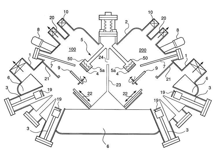
The shown film deposition apparatus basically includes a vacuum
chamber 2 comprising twin deposition rooms 100 and 200 symmetrically
arranged and communicating by a through hole 24 on a bulkhead 23 with
each other. The deposition rooms 100 and 200 are designed in the same
way excluding the symmetrical arrangement.
Each of the deposition rooms 100 and 200is provided with a main
evacuating apparatus 1, at least one K (Knudsen's) cell 3 provided at a
bottom of each deposition room as an evaporation source or a molecular
beam source. A bifurcate sample holder 5 is provided at a top of the
vacuum chamber 2, where each head 50 holds a substrate 4 on which a
2 5 film is to be deposited. The bifurcate sample holder 5 is rotatable around
a symmetrical axis of the vacuum chamber 2 so that the heads 50 can be
aligned at deposition positions in the deposition rooms 100 and 200. The
213~12~
bifurcate sample holder 5 is associated with heaters Sa for heating the
attached substrates 4 to its heads S0. Liquid nitrogen shrouds 6 for
forming cold traps are disposed at a bottom of the vacuum chamber 2 and
around evaporation sources of the K cells 3.
In addition, each of the deposition rooms 100 and 200 is also
provided with a port 10 for exchanging a sample, and a RHEED
(Reflecting High Energy Electron Diffraction) device 8 for evaluating a
film surface roughness during the deposition. In front of the substrate 4
attached to the head S0 of the sample holder S, a shutter 9 is located for
controlling a deposition time during the deposition process. The K cells 3
are also provided with operatable shutters 19.
Additionally, a gas supplying apparatus 7 is provided so as to
introduce an oxidizing gas such as 2, 03, NO2, N2O, etc. in vicinity of
the substrate 4 attached to the head S0 of the sample holder S, so that the
l S oxidizing gas can be supplied to form an oxygen-enriched atmosphere in
the vicinity of the substrate 4 in order to oxidize molecular beams
incoming from the evaporation source in the course of the film
deposition.
Furthermore, each of the deposition rooms 100 and 200 of the film
deposition apparatus additionally includes a partitioning plate 21 for
dividing the vacuum chamber 2 into a first sub-chamber which is
constituted of a lower portion of the vacuum chamber defined below the
partitioning plate 21 and which is coupled to the K cell 3 and the main
evacuating apparatus 1, and a second sub-chamber which is constituted of
2 5 an upper portion of the vacuum chamber defined above the partitioning
plate 21 and in which the head S0 of the sample holder S is located. The
partitioning plate 21 includes a through opening formed at a center
- 10 -
2135125
thereof. The position of the opening is determined to ensure that a beam
emitted from K cells 3 toward the substrate 4 is not obstructed by the
partitioning plate 21. In addition, the size of the opening is determined to
enable restricted molecular flows, particularly oxidation gases, from the
second sub-chamber to the first sub-chamber so that a pressure difference
can be created between the first sub-chamber and the second sub-chamber
even if the opening is open. Therefore, the partitioning plate 21 having
the through opening constitutes a vacuum conductance.
A gate valve 22 is provided on the partitioning plate 21 for
hermetically closing the opening of the partitioning plate 21, so as to
completely shut off the molecular flows between the first sub-chamber
and the second sub-chamber when the gate valve 22 is closed. An opening
and closing of this gate valve 22 is controlled from the outside of the film
deposition apparatus by a not-shown means.
In addition, an auxiliary evacuating apparatus 20 is coupled to the
second sub-chamber for evacuating the second sub-chamber to an ultra-
high vacuum when the gate valve 22 is closed. The auxiliary evacuating
apparatus 20 is constituted of a cryopump. On the other hand, the main
evacuating apparatus 1 is constituted of a diffusion pump.
2 0 The above film deposition apparatus comprises the two deposition
rooms 100 and 200. However, the number of deposition rooms are not
limited two. The film deposition apparatus may comprise more than two
deposition rooms.
Referring to Figure 2 there is shown a diagr~mm~tic sectional view
2 5 of a second embodiment of the film deposition apparatus in accordance
with the present invention.
213~125
The shown film deposition apparatus basically includes a vacuum
chamber 2 similar to the deposition rooms 100 or 200 of Figure 1
provided with a main evacuating apparatus 1, two sets of K cells 31 and
32 provided at a bottom of the vacuum chamber 2, and a bifurcate sample
5 holder S provided at a top of the vacuum chamber 2, each head 50 of
which holds a substrate 4 on which a film is to be deposited. The heads
50 of the bifurcate sample holder S hold substrates 4 so as to face
different directions. The substrates 4 respectively correspond to the sets
of the K cells 31 and 32 when the heads S0 are situated at deposition
10 positions. Namely, K cells 31 are arranged to concentrate emitting
molecular beams on a left side substrate 4 so as to deposit a thin film on it
and K cells 32 are arranged to concentrate emitting molecular beams on a
right side substrate 4 so as to deposit a thin film on it when the heads 50
are situated at the deposition positions. Each head 50 of the bifurcate
1 5 sample holder S is associated with a heater Sa for heating the substrate and shield 5b avoiding incidence of molecular beams from a
non-corresponding set of the K cells. The bifurcate sample holder 5 is
rotatable on its axis so that the heads 50 can be located at the both
deposition positions corresponding to the sets of the K cells 31 and 32. Of
20 course, the sample holder S can branch into three or more so that each
branch has a head corresponding to a set of K cells.
In addition, the vacuum chamber 2is also provided with a port 10
for exchanging a sample, a liquid nitrogen shroud 6 for forming a cold
trap around evaporation sources of the K cells 31 and 32. In front of the
2 5 substrates 4 attached to the heads 50 of the bifurcate sample holder S0,
shutters 9 are located for controlling a deposition time during the
deposition process. The K cells 31 and 32 are provided with an
213512~
operatable shutter 19. There also can be provided with a RHEED device,
as shown in Figure 1, for evaluating a thin film surface roughness during
the deposition (not shown in Figure 2).
Other parts of this film deposition apparatus is the same as those of
the deposition rooms 100 or 200 of Figure 1 so that explanation can be
omitted.
Example
A layered structure of a lower thin film of YlBa2Cu307~ oxide
superconductor and an upper thin film of SrTiO3 dielectric oxide was
formed on a SrTiO3 (100) substrate by using the apparatus of Figure 1.
At first, a SrTiO3 (100) substrate 4 was set to the head 50 of the
sample holder 5 located at the deposition room 100, and metal yttrium,
metal barium and metal copper were set to three K cells 3 of the
deposition room 100 as evaporation sources. A dummy substrate was set
to the other head 50 of the sample holder 5 positioned to the deposition
room 200. Metal strontium and metal titanium were set to two K cells 3
of the deposition room 200 as evaporation sources. Thereafter, the
chamber 2 was closed and the gate valves 22 were opened. The deposition
rooms 100 and 200 of vacuum chamber 2 were evacuated by the main
evacuating apparatuses 1 and the auxiliary evacuating apparatuses 20 to an
ultra-high vacuum of which the pressure was lower than 1 x 10⁻¹⁰ Torr
in which background pressure the film deposition by the co-evaporation
process was conducted. Succeedingly, 2 gas including more than 70
2 5 volume percent O3 was supplied from the gas supplying device 7 of the
deposition room 100 so that the pressure in the second sub-chamber of the
deposition room 100 became 5 x 10⁻⁵ Torr. As mentioned above, the
- 13 -
_` 213~i25
deposition room 100 was provided with the vacuum conductance (the
partitioning plate 21 having the through opening), a pressure difference
of about one digit or more was created between the first sub-chamber and
the second sub-chamber. In addition, the oxidizing gas injected from the
5 gas supplying device 7 was irradiated onto a deposition surface of the
substrate 4, the pressure of the oxidizing gas on the deposition surface of
the substrate 4 was maintained much higher.
Then, the substrate 4 was heated by the heater Sa to a temperature
of 700 C. The K cell 3 of metal yttrium was heated to a temperature of
10 1220 C, the K cell 3 of metal barium was heated to a temperature of 620
C and the K cell 3 of metal copper was heated to a temperature of 1000
C. Precise control of each flux of the molecular beam was conducted by
way of adjusting crucible temperature for stoichiometric deposition.
When the influx of the molecular beams had become to be stable from the
l S evaporation sources after the shutters 19 were opened, the shutter 9 of the
deposition room 100 was opened so as to start deposition of the oxide
superconductor thin film onto the substrate 4. At this time, a surface
roughness of this deposited film was evaluated by the RHEED device.
The oxide superconductor thin film was grown up to a thickness of 50
20 nanometers at a deposition rate of 1 nanometer/minute. The deposition
rate is preferably 0.5 to 2 nanometers/minute.
Until the oxide superconductor thin film was finished to be
deposited in the deposition room 100, the K cell 3 of metal strontium was
heated to a temperature of 520 C and the K cell 3 of metal titanium was
25 heated to a temperature of lS00 C so as to generate molecular beams
with stable operation for stoichiometric deposition. The temperature of
metal strontium is preferably 450 to 600 C and the temperature of metal
- 14 -
2135123
titanium is preferably 1430 C to 1550 C. In addition, 2 gas including
more than 70 volume percent 03 was supplied from the gas supplying
device 7 of the deposition room 200 so that the pressure in the second
chamber of the deposition room 200 became 3 x 10⁻⁵ Torr.
When the oxide superconductor thin film had reached a thickness of
50 nanometers so as to complete deposition of the oxide superconductor
thin film, the sample holder 5 was rotated to transport the SrTiO3 (100)
substrate 4 on which the superconductor thin film was deposited to the
deposition room 200. The substrate 4 was cooled down to a temperature
of 480 C the shutter 9 of the deposition room 200 was opened so as to
start deposition of the SrTiO3 dielectric film onto the oxide
superconductor thin film. The substrate temperature is preferably 430 to
580 C.
At this time, a surface roughness of this deposited film was
evaluated by the RHEED device. The dielectric oxide thin film was
grown up to a thickness of 250 nanometers at a deposition rate of 1.2
nanometer/minute. The deposition rate is preferably 0.5 to 2
nanometers/minute .
When the dielectric oxide thin film has reached a thickness of 250
nanometers, the substrate 4 was cooled down to the room temperature.
While the substrate 4 was cooled down, oxygen supply was m~int~ined in
the condition in which the dielectric oxide thin film was deposited.
After the layered structure of the oxide superconductor thin film
and the dielectric film was obtained, crystal structures, surface and
2 5 interface properties of the layered structure was were evaluated by LEED
and XPS without exposing the oxide superconductor thin film to the air.
It was confirmed that the oxide superconductor thin film was a c-axis
~135~Z5
orientated YlBa2Cu307 ~ oxide superconductor thin film and has high
crystallinity. It was also revealed that the dielectric oxide thin film of the
upper layer of the layered structure had a crystalline smooth surface and
an interface between the oxide superconductor thin film and the dielectric
5 oxide thin film was defined sharply.
As explained above, a layered structure of an oxide superconductor
thin film and a thin film of a different material or composition having an
excellent surface cleanness and roughness, high crystallinity and a sharp
interface can be obtained by the process using the apparatus in accordance
10 with the present invention. It can be also used more than three layer
deposition, which can reduce the interdiffusion between bottom layers.
The layered structure can be favorably applied to superconducting
devices.
The invention has thus been shown and described with reference to
15 the specific embodiments. However, it should be noted that the present
invention is in no way limited to the details of the illustrated structures
but converts and modifications may be made within the scope of the
appended claims.
- 16 -