Note: Descriptions are shown in the official language in which they were submitted.
21~304 ~-`
93/23921 PCT/GB93/009~4
METHOD AND APPARATUS FOR AMPLIFYING. .
~Q~ATIN~ AND_DEMODULATING
The present invention relates to method and circuits for -
processing components of an inp`ut signal to provide a highly
efficient linear amplifier and/or modulator or a demodulator.
A LINC amplifier has been proposed (see D.C. Cox, "Linear
Amplification Using Non-Linear Camponents", IEEE Transactions on
Communications, Vol. COM-22, 1974, pages 1942 to 1945) in which a
modulating signal is split into two phase modulated components with
constant envelopes which can be amplified separately using highly
non~linear but power efficient amplifiers. Combining the two
output signals yields the desired linearly amplified signal. With
a LINC amplifier the potential for dc to RF conversion efficiency
can approach 100~, assuming ideal matching amplifiers. However, in
practical LINC amplifiers, the suppression o~ broadband phase
modulation relies on a very tight tolerance on the gain and phase
match between the two paths. A gain error of 0.01 dB and a phase
error of 0.1 give a component suppression of only 54 dB. Such a
tolerance is impossible to achieve in a open loop system where much
20; greater gain and phase variations can4 occur with changes in
operating frequency, output power and temperature, and the ageing
or components.
It ls an obJect of this invention to provide a linear
amplifier/modulatc,r which does not suffer signi~icantly from these
~ problems.
From GB 2073516 an~ arrangement for amplifying a previously
modulated carrier~signal using two phase locked ioops is already
: known and in which phase feedback and phase comparators are used~
In~ one' embodiment~ the~ feedback signals are taken from a point
; ~ i 30 before the final; summlng circult. In prac~ice the summing circuit ~ ,
will~ be lmperfect and~ any phase errors introduced by the summing
; circuit will degra~de the performan~ce of the system. The input~
s~1gnal~ is~ at;or~near the same ~frequency~as the output signal and~ ~ ¦
where the output i~s to be at radi~o~frequencies~(RF) implementation
21 3 5 ~`0 4
,
of the summing circuits 14 and 15 is, in practice, complicated.
5uch an arrange,~ent could not receive a baseband signal and
incorporate modulation of that signal within the phase loeked loops.
In a second embodiment of GB 2073516, the feedback signal is
taken from a point after the final summing circuit. However
comparisons ffhfith the input signal are made in terms of the
amplitude and phase and, when the input is at RF, such a system
requires accurate RF envelope detection and subtraction and a wide
dynamic range RF phase detector. Such devices are difficuflt tv
10 construct. ` `
,
~ From US 5105168 an arrangement for a vector locked loop for
modulation of an input slgnal is already known. US ,5105168
incorporates a mixer in the feedback path so that comparisons may
be fmade at or near the lnput si~inal frequencyff which may be a
baseband signal with an output signal at RF. However the
realisation of envelope detectors for such an arrangement presents~
problems as they requtre subsequent flltering of the carrier
components, which intrQduces an unacceptable amount of time delay.
Additional signifficant. time delays ar~ introdffffced by the phase
detector which ifS requlred to generate the dlfference component and
the filter which is~required to remove the sum component. ~ :
It ls another object of the ifnvent~ffon to provide an
amplifier/modulator whlch may use the Cartesian components of an
input signal. The advantage~ of the a; Cartesian signal is that a~
representation of the signal can be produced with a low sampling
rate, especially when~derived by a digital signal processor (DSP).
It ls a furt~her object of the invention to provide an
!ampli~ier/n~fdulfator which incorporatesi modulation, ampliflcat`if~ffn `
and summa~tion ffffffithin a feedback loop, so that~there is compensation
for~any~ deficienc~ies in~the~system.~
According to ~one aspect of the~;~invention there is provided ~ :
apparatus for proc~e~ssing components o~ a~n ~nput signal~to provide~a
processed'~ffutp~fft~:sifgnal, comprisi:ng~
;flrst and~ second~ feedback~ control loff-ffps for generating, i~n
35~ re~sponse~to the lffnput signal;, respective components o~ a processed
output~ si~gnal,~or ~for ;use in:~gener;ating the` processed output
;. _3
l..
2135304
signal, and for ensuring that the components are in a correct phase
relationship with each other for this purpose,
each loop comprising means for generating a loop output signal
having a frequency or phase which is variable in response to a
control signal, and which forms one of the components of the
processed output signal, or fram which one such component is
derived, and a comparator for generating the control signal, and
means for combining the loop output signals in deriving a
resultant signal, and
means for. providing f'irst and second feedback signals,
dependent on the resultant signal and in phase quadrature with one
another,
the feedback signals being applied to one input of the
comparators of the first and second loops, respectively, and
another input of eaeh comparator being coupled to receive a
reference signal indicative of a desired value of .the control
signal.
Atcordlng to a second aspect of the invention there is
provided a ~ethod of processing the 'com~onents of an input signal
to provide a processed output signal by using first and second
feedback con~rol loops to generate, in response to the input
signal, respectlve co~ponents of the processed output signal, or
for use in generating the processed output signal, and for ensuring
that the components are in a correct phase relationship with each
Z5 other for this purpose, comprisin~
~: generating a loop output signal for each loop having a
frequency which is variable in response to a respective control
signal andi which ~forms o'ne of the components of the' processed
output signal, or from which one such component is derived,
combining the loop ou~put signals in deriv1ng a resultant
signal, .
generating ~eedback signals from the resultant signal in phase
~ ' quadratu~e with one another, one for each loop, and
: : comparing each feedback signal with a respective reference
: 35 ' signal to provlde the~respective control signals.
:~ ~ Processing carried out by the invention 'may, for example, be
i; J ;,j;`
213S~O~ `
W O 93/23921 `~ PCT!GB93/0095
. . ! !
modulation and/or ampliflcation, or demodulation.
The feedback signals may be provided by mixing the said '
resultant signal with respective quadrature signals from an
oscillator. : .
Where modulation is to :be carried out, the Cartesian
components of the input signals may be applied as the reference
signals and the said resultant signal is the modulated output
signal in which a :signal at the frequency of the oscillator is
: modulated by the input signal, that is freq'ueney translation of the
: 10: input signal to the frequency of:the oscillator occurs.
for amplification, each loop contai:ns an amplifier to amplify~ :
: the loop output signals~ before they are~ combined, and~ if any~:
amplification without modulation is required, then :the: oscil,lator
out~ut frequency is set to zero. ~ `
15 ~ ~:To achieve demodulation the loop output signals are combined ' '
with a modulated si:gnal in ~such a way that:frequency translated~
si~gnals derived from the resultant sign:al indicate: any frequency or
ph~se~ devlations' ;of :~the~ loop output ~s~ignais::~from respective~
compone~nts of the~'modulàted signal.~ Also a zero ~agnitude ~signal
20 ls`~applied as the~ respec:tive; referencP~signals,:~for example::by;~
grounding ;one input~terminal~:~of~ e~ach: comparator, and :the loop~
:output: signals~a~re~.;demodulated us~ing the respective quadrature~
components:of the~os;ci.llator ~output~signals~ to provide components;~
;:of~:the output sl~g:nal~wh~lch~can then:be comblned in~a known~way t;o~
~.derive a slgnal~ representativ~e~:of the~modulatlon of the modulated~
: One:~of~the~:main`advantages of the circuit is ~that i~:~ allows~
components of an ~o!utput ,slgnal,: or a~s1gnal,i,~rom ~whlch:lsulch,
`: components can::be~ derived, to be~generated~:and'~combined:withi:n;~a ;
30~.con~tro1~ loop~so ~ hat;~:~problems~o ';errors~;~in:~comblnation~ are~
s1~gnlfl~cantly~redu~
'~n~ Ot~her ;a vant gè~s:~:~wh~c~h~:~m ~.~be~ ach:ie:ved include~ maximising: the~
e len~cy~ the odulat ~/amp~l;lf~ p~artlc`:larly ~when used;~ n~a~
` t .~ th ~a ~ to~constr ~clrcul~ts~according;to~the~
~ ~13~30~
93~39~1 PCT/GB93/009~4
invention with readily available, low cost, low tolerance
components, and minimising or eliminating the use of complex
digital signal processing.
The demodulator also allows a variable strength input signal,
such as might be received by a radio system, to be converted to two
phase modulated components of constant amplitude which are easier
to process.
It is believed that the input andJor output signals may be
represented by other component systems thah Cartesian components.
For example polar components or non-rectangular components may
possibly be used.
- Embodiments of the invention will now be described by
reference to the following drawings, in which:- ;
Figure 1 is a block diagram of an amplifier/modulator
lS embodying the invention,
Figure 2 is a block diagram of a demodulator embodying the
invention, and
Flgure 3 ls a diagram showins regions of stability for
Flgure 1,
Figure 4 is a block diagram of ~nother amplifier/modulator
embodying the invention,
Figure S is a block diagram of a third amplifier/modulator
embodying the invention,
Figure 6 is a block diagram of an amplifier embodying the
invention
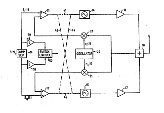
In Figure 1, an input signal s(t) having for example amplitude
or phase variations, or both, is separated by a known component
separator 10 into two component signals which vary in amplitu,de and~
phase~ but àre in phase quadrature. These two components, sj(t) and
30 Sq(t) are the Cartesian components (I and Q) of the input signal
and each component signal is passed to one of two feedback loops.
As an alternative the input signal may be supplied in the form of
separate I and Q signals. The first element in each loop is a
comparator ~11 and 12) and each component signal is passed to the
` ~ :
~`~
2135304
, ~, `. `
- 6 -
non-in~erting input of the eomparator. The output signal of this
comparator is passed in this example by way of connections 41 and
42 (which can be selected ~rom connections 41 to 44 as is described
below) to control the frequency of a voltage controlled oscillator
(VC0) (14 and 15) and the resulting output signal is amplified by
an a non-linear radio-frequency amplifier (16 and 17). The output
signals from the amplifiers are comb'ined by a summing circuit 18
to produce as ~s explained below a frequency translated amplified
version of the input signal s(t) at the frequency of the
oscillator 22. : ~ `
~Feedback control is created for each loop by taking the output
of the summing circuit 18 demodulating that signal with a signal
rj(t) and rq~t)) at a mixer (20 and 21) and passing the resultin~
feedback signal to the non-inverting lnput of the comparator of
~15 that loop. The ~signals r1~t) and rq(t) supplied to each mixer are
the quadrature :Cartesian components of a signal r(t) from an
~ oscillator 22 and the frequency difference between the modulated
`;; ~ : ~ signal at the output of':the summlng circult 18 and thè input to the
component separator ~lO equals the freque~cy of the oscillator 22.
Z0~ ' ; In operatton ~the output of the mixer 20 for example i5
compared by the :comparator ll with ~the signal sj~t) and any
dl~fference assuming:;~the dlrect connections 41: and 42 are~ made~
.` controls'the ~requenc:1es gene.rated by the~:VC0 .14~ sa that its output
slgnal~ls :such:~that:~when:~s~ummed~ ~ith the output of the VC0 15 and~
2~5~: demodul~ated~ by~ the~ mix~er 20 1t forms~a replica of:~sj~t).~ In~a
s:imilar:way~:the~output~signal ~of the VC0 15 when~summed with the
~: output of the VC0~1~4 and~demodulated by the mixer 21 i:s~a~repl1ca
of~ Sq(t)` ~Thusl~when the outpu`t s1gnals~of the' vcos 14i:and 15~are
combined by the~summing c1rcuit~;18 they~ provide a~si~gnal ~:at::~the
~30~: reference~ frequency:::wh~ic:h~ s~ a~::fr~uen:cy trans~lated ampli:~ied
j~ u ~vers1on of s~lt)~ ;'assum~ng~that~:the de ~ d~ulat10n;processes are~exact~perPect ~gai~n~ and~:~pha~se`~ mat:ch~ing~:and that ~the loop ;gain is:
n~ln~ite ~gi~ ing~feed~back ~con~trol~:loops wi~h error:~s~1gnals of zero.
:S~ince ~the~amp1:~tudes~of~the~ outputs of the~VCOs~:are~:inh'ere~ntly
AM~NDED SHE~T
'." :?, 21 3 5 3 0 ~ '
93/;~39;~1 PCl'/(;;~93/009~i4
constant the amplifiers 16 and 17 can be non-linear, for example
Class C, so that high efficiency amplification and modulation can
be achieved. By providing feedback control the frequency and phase
of each signal from the VCOs 14 and 15 is controlled to ensure that
S gain and amplitude matching is as required in combining these
signals as components of the required output signal from the
summing circuit 18. Deviations in gain as well as phase are
corrected by phase variations in the signals combined caused by the
action of feedback.
10Where only modulation is required the amplifiers 16 and 17 can
be omitted or of unity gain. Where only amplification is required,
without frequency translation, then the frequency of the
oscillator 22 is set to zero. For example the oscillator 22 and
the mixers 20 and 21 may be omitted when the signals from the
15summing circuit 18 to the comparators 11 and 12 are arranged to be
in phase quadrature, with the comparator 12 receiving a signal with
a 90 phase shift, as described below in relation to Figure 6.
The modulator of Figure 1 can be viewed as a combination of
two analogue phase locked loops and a basic ùnderstanding of the
factors affecting system per~ormance can b~ drawn from conventional
phase locked loop theory. Loop gain will in practice be limited by
stability of the feedback process, and loop capture range ~ill
dictate the ultimate modulation bandwidth.
Figure 3 is a diagram in which a vector 45 represents the sine
signal rq(t~ from the oscillator 22 and a vector 46 represents the
cos~ne signal rj~t). It can be shown mathematically that, if the
connections 41 and 42 are as shown in Figure 1 without any signal
invelrsion, thelst~bl,e region of lock for the combined loop system
covers the semi-circle 49. This in effect limits the application
of the modulator to formats such as full carrier amplitude
modulation and amplitude shift keying.
~ limited performance in one quadrant does not provlde a
universal modulator and stable operation in all four quadrants can
be ach~eved if the sign of the feedback components is controlled as
'
213S:30~ -:
W 0 93/Z3921 pcT/&B93/oq9s4 ~ i
a function of the sign of the signals sj(t) and Sq(t).
In order to determine the sign of si(t) and Sq~t)~ the t~o
outputs of the component separator 10 are coupled to comparators S0
and 51, respectively, with each comparator providing a logic 1 for
S a positive input and a logic 0 ~or a nec?ative input. These logic
signals are applied to a switch control circuit 53 which controls
the connections 41 to 43 and whether inversion is to occur within
these connections. Such connections may be provided by known
circuits. A number of connection schemes are suitable for
four-quadrant stable operation and one is given in the following
table, by way of example, where a pri,ned connection designation,
for example 41 ' t indicates signal inversion and designations
without primes indicate no inversion.
- .
sl(t) Sq(t)To VC0 14To VC0 lS
1 1 44 43
1 0 41 42
0 1 41' 4~
0 0 ~44' ~3
.
It may be shown, mathematically, that the stable region of
lock for the combined loop system covers more than quadrant 48 and
extends further to include the area up to line 48a.
Figure 2 shows a demodulator according to the invention, in
which an input signal to be demoduiated is received by a summing
ci.ncuit 25 ,firom ~a source in this example illustrated by an
antenna 26 but which could be any modulated signal source. When
VCOs 27 and 28 are operating at exactly the frequencies and phases
of components of the lnput signal. the input signal is cancelled ln
the summing circuit 25. At other times a small error sig?nal
reaches demodulators 32 and 33 where Cartesian components of the
; error signal are generated using quadrature reference signals rj(t)
.
:~ :
2135~0~
; .
W O 93/23921 PCT/GB93/~
and rq(t) from an oscillator 34 at the ~requency which carries ~e
modulation to be detected (that is the carrier frequency)~ Th~s~
Cartesian components, which should be zero when perre~
cancellation occurs in the summing circuit 25, are compared ~h ~
zero magnitude signal in comparators 35 and ~6 obtained ~y
grounding the non-inverting inputs of these comparators. and t~e
outputs obtained control the frequencies of the VCOs 27 and 28. ~s
a result the output frequencies of these VCOs are replicas of the
components of the input signal to the demodulator and are d~wn
converted by demodulators ~7 and 38 using the respective quadrature
outputs of the oscillator 34 to provide demodulated components of
the modulation of the carrier signal. These components ca~ be
combined in a known way to provide a frequency translated replica
of a radio-frequency input signal at thè antenna 26.
15Problems of stability also arise with the demodulation circuit
and can be overcome by the use of ~he same switched connections as
those of Figure 1 controlled by the signs of the outputs of ~h~ '
demodu'lators 32 and 3~.
Amplifiers 29 and 30 are shown in Figure 2 at the outputs of
the VCOs 27 and Z8 and are useful in correcting levels. To this
end the gain of these amplifiers may be greater or less than unity,
and in some circumstances they may not be required.
Figutes 4 and 5 show embodiments of the invention which
~aintain stability in all four quadrants. The input signal is
confined to the quadrant where the amplifier/modulator is stab~e
and the necessary phase shift is added back to the output signal.
~`In figure 4 an input signal Aei~, having for example amplitude
o,r,!phase variiatio,ns,~ or both, is separated by a~ known compdnent l`
separator 61 in a manner as described in relation to ~igure 1.
Alternatively the input signa! may be supplied as separate I and
signals, COSa an,d sin. Each component signal is passed to a phase
shifter 62 which; shifts the phase of each signal by a facto~
which is the difference in phase between the input and the o~tput
signals. The absolute value o~ each phase shifted input component
~::: :
~.
2135~04 ` ~
W O 93/2~92t pcT/GB93/qo954
., ~
'`.. ` i~ - ;.
signal is taken by the 'rectifier' circuits 63 and 64, leaving a
signal containing mainly amplitude information. This ensures that
each component signal is kept in a region for which the combined
system is stable, as illustrated by quadrant 48 of figure 3 and ~ :
described above. The output signals o~ the rectifiers are passed
to the inverting inputs of the comparators 65, 66 in the latter
a~ter inversion. The output signal of the comparator controls the
frequency of a VC0 67. 68 via switchable connections 69, 70, 71 and
72. The resulting output signal may be amplified by a non-linear
RF amplifier 73, 74. As before these amplifiers may be omitted or
of unity gain where only modulation is required. The outputs of
the two amplifiers are combined by summing circuit 75 to produce a
frequency translated amplified version of the input signal.
Feedback control is provided for each loop in a similar manner
to that used in the embodiment illustrated by figure 1, by
demodulating the output of the summing circuit 75, Bei(~+~t) with
quadrature signals cos(~t), sin(~t) produced by the oscillator 76
at the mixers 77, 78. The phase of each input component is added
back into the feedback loop by shifting the demodulated component
of the output signal with the phase of ~he component of the input
signal at a phase shifter 79; thus the signal rrom the mixer 77, 78
are shifted in phase by a factor ~-~. The feedback loop is
completed by passing the resulting signal to the, non-inverting
input of the comparator. The frequency difference between the
output signal and the input signal is that of the frequency of the
oscillator 76.
Figure 5 is a simplified version of the amplifierlmodulator
shown in ~i,gure 4. An input signal Aej, of the type d~escribed in
relation to figure 4 is separated by a known component separator 85
in a manner as described in relation to figure 1. The absolute
val~ue of the input signali ie the amplitude information, is
selected by a 'rectifier' circuit 86 and this value is passed into
the non-inverting input of a comparator 88. The phase component of
each signal is selected by circuit 87 which limits each component
35 signal to unity, with phase information. The non-inverting input
2135~0i
~`
W`O 93/23921 ~ B93/00954
of a comparator 89 is grounded and thus the output of the
comparator mirrors the input of the non-inverting input. The
output signal of the comparator 88, 89 controls the frequency of a
VC0 90. 91 via switchable connections 92, ~3, 94 and 95. The
S resulting output signal may be amplified by a non-linear RF
amplifier 96, 97. As be~ore these amplifiers may be omitted or of
unit gain where only modulation is required. The outputs of the
two amplifiers are combined by summing circuit ~8 to produce a
frequency translated amplified version of the input signal at the
frequency of the oscillator 99.
Feedback control is provided for each loop in a similar manner
so that used in the embodiment illustrated by figure 4, by
demodulating the output of the summing circuit 98, Be j(~+~t~ with
quadrature signals cos (~t), sin(~t) produced by the oscillator 99
at mixers 100, 101. The phase of each input component is added
back into each feedback loop by shifting the demodulated component
of the output signal with the,phase of each omponent of the input
signal at a phase shifter 102. The feedback loop is completed by
passing the resulting signal to the non~inverting input of the
comparator. The frequency difference bet~ween the output signal and
the input signal is that o~ the frequency of the oscillator 98.
Although the input to the loops is constrained to be within
the stable region of the systemi VC0 switching may be required to
~ reduce impulse noise generated by the VC0. When the envelope of
:25 the input signal crosses zero (hereafter 'zero crossing') the phase
of the input signal changes by 180 and this can be illustrated by
plotting a vector of the input signal onto figure ~. ~hen the
enlvelope cro$ses, zéro the vector will cross from one quadrant:to~
the diagonally opposite quadrant and wi 11 pass through the origin.
The output of the VCOs, when summed at the swimming junctiQn,
~, 'produces a similar signal to that of the input and thus when the
': input phase changes by 180 the output will also change by 180.
~: :Since the output is created by summing the output of the two VCOs,
i t can be shown that the output of each VC0 needs t~ change by 180
~:
Z1353 ~ !~ r
WO g3/2392 1 PCl /GB93JO(~
- :
. ;. ' .
_ 12 -
as well. The VOCs introduce a finite delay into the system ~nd
also generate an impulse noise. Figures 4 and 5 include a phase
detector 105 and a differentiator 106 which in combination produce
a signal when the phase changes by 180. The output of the
differentiator is coupled to the non-inverting input of a
comparator 107, the inverting input of which is coupled to a
reference signal. When the output of the diFferentiator crosses a
threshold, which is that of the reference signal, the input to the
VCOs are switched by the switching connections, (69. 70, 71 and 72
in figure 4 and 92, 93~ 94 and 95 in figure 5).
The embodiment illustrated in figure 1 will also generate
impulse noise when zero crossing occurs. For clarity the phase
detector, differentiator, comparator and further switchable
connections have been omitted. Alternativély the switch controls
may take into account zero crossing and switch accordingly.
I~ the system is to amplify without modulation (if the
oscillator is set near to or at zero) an alternative arrangement is
needed to create suitable phase quadrature feedback signals.
Figure 6 is an illustration of a modified version of the embodiment
of the circuit shown in figure 1, whi~h works substantially as
described above. Similar arrangements may be applied to the
embodiments illustrated in figures 4 and 5. An input signal of the
type described in relation to figure 1 is separated by a component
separator, as described above. The component signals are passed to
the inverting input of the comparator 111, 112, the output of
which is connected via switchable connections (as described in
relation to figure 1) to a VCO 113, 114. The VCO generates at its
output two s;ignals I~and Q, which are in phase quadrature withjeach~
other. The Q signal of each VCO (113, 114) is summed by summing
circuit 115. One output of the summing junction forms the feedback
lo~p and is passed to the non-inverting input of the comparator
112. The I signal of each VCO (113, 114) is summed by summing
circuit 116. One output of the summing junction forms the feedbac~
loop and is passed to the non-inverting input of the comparator
. . .
212J53~I
93/23921 PCl /C~B93!0~9~4
111. The other outputs of the summing junctions 115, 116 are
passed to amplifiers 117 and 118 and the amplified signals are
summed by summing junction 119. Switch control for the VCOs may be
provided in the same manner as described in relation to figure 1
S and zero crossing switching may also be applied if desired.
Some alternative arrangements relating to figure 6 will now be
mentioned. In the first, the amplifiers 117 and 118, and the
summing junction 119 are omitted, respective substitute amplifiers
are connected in the I signal paths between the VCOs 113 and 114,
and the summing junction 116, and the output signal is taken from
the summing junction 115. The substitute amplifiers may instead be
~ in corresponding positions in the Q signal paths. In both cases an
attenuator or a futher amplifier is required to ensure that the two
feedback signals are at corresponding levels at the comparators 111
lS and 112. Substitute amplifiers may be used in both I and Q paths
at the VC0 outputs. Such arrangements have the advantage that the
substitute amplifiers are included in the feedback loop before
summation to provide the output signal. The amplifiers 117 and 118
andtor the summing junction 119 may be used in addition to the
substitute amplifiers in any of ~he substitute amplifier
` arrangements.
It will be realised that the invention can be put into
operation in ~any other ways than those specifically described.
For example the VCOs may be any form of frequency generator having
an output signal which can be controlled using a control signal,
for example some forms of unstable ampli~ier or direct digital
~ synthesizers.
; The switching matrlces of figures 1, 4, 5 andi 6 may in some
' ` situations be replaced by permenant connections which give a stable
arrangement and prevent impulse noise on zero crossing.
Since Cartesian components of an input signal, and some
alternative kinds of components, are phase modulated, the invention
can handle any other ;types ~of modulation in addition to those
mentioned.
~ ,
. :
;.: ~ : .