Note: Descriptions are shown in the official language in which they were submitted.
~" 2~3~321
LM 5910
An interface circuit between a four wire line and a two wire line -~
Field of the Invention and Backaround of the Invention.
The present invention relates to an interface circuit between ;
a four wire line and a two wire line, including a four wire
interface with a receive input and a ~send output, as well as a
two wire interface including two terminals facing the two wire `~
line, one for each wire. An output amplifier is located before
each terminal. First circuit means apply, via the amplifiers, a
signal received on the receive input as a differential signal on
said terminals of the two wire intexface. Second circuit means
feed to the send output a differential signal received on said ~ ;
terminals of the two wire interface from the two wire line. Third ~-
circuit means form a longitudinal signal by means of the sum of
voltages appearing on each of said terminals. A feed back~loop `~
extends to each amplifier for an adjustment signal which is
derived from the longitudinal signal, for adjusting the
impedances of the two wire interface to earth, the so called
longitudinal terminating impedances so as to attain longitudinal ~
balance. ~ ;
Generally, a subscriber line is connected to a telephone
exchange office via a so called two wire interface. The telephone ;~`~
exchange office is connected to other telephone exchange offices ;
via a so called four wire interface. Two of the wires are used
for sending speech signals to other exchange offices and the ;~
other two for receiving speech signals from other exchange ;~;
offices. ~ ``
A speech signal which is received on the four wire interface
is passed on to the two wire interface where it appears as a ;~;
transversal (differential) signal. If a transversal signal
arriving from the subscriber appears in the two wire interface it
will be passed on to the four wire interface and possibly further ;~
on to another exchange.
Today, integrated circuits are used for performing the
transformation between the two and four wire interfaces. Such a
circuit usually is ~enominated SLIC, Subscriber Line Interface `'~
Circuit. There are very high demands put on the SLIC that its so `
called longitudinal terminating impedances should be equal, i.e.
;~J ' ~
13~32~
.
the impedance from the two wire interface to earth should be
equal for the wires of the two wire line. ~ `
External disturbances, e.g. from the power network or caused
- by a thunderstorm, may give rise to 50 called longitudinal
signals on the two wire line. Besides that these longitudinal
signals may disturb the speech signals, they may also give rise
to harmful voltages in the two wire interface. Inversely,
transversal signals, e.g. speech signals, may give rise to
longitudinal signals. This may cause cross talk to two wire lines
located nearby.
Description of Related ~rt.
In order to obtain longitudinal balance good enough in a
SLIC, trimming of amplifications in a number of signal paths has
been used, cf. the Swedish patent 448,264, which discloses a
circuit essentially of the kind defined by way of introduction.
The trimming may be performed in several ways during the
manufacture, e.g. by trimming thin film resistances by means of a
laser.
A circuit likewise of essentially the kind defined by way of
introduction is disclosed in the European patent
0,134,229, in which a method is described for automatically
trimming the circuit in its location in the exchange office. More
particularly, this method requires that the circuit is put into a
trimming state, whereupon a number of signal connecting up and
measuring operations followed by trimming adjustments are
performed.
As an example of the general state of the art the following
patent publications may besides be mentioned: SE-B 446,579, EP-A2
272,800, US-A 4,387,273 and W0-A1 90/01837.
Summary.
ne object of the invention is to enable with simple~means,
in a circuit of the kind defined by way of introduction, that
adjustments of the longitudinal balance to maximum may be
performed continuously when the circuit is in operation.
The circuit according to the invention comprises correlator
and control circuit means connected for receiving the ~
longitudinal signal and a transversal signal corresponding to the ~;
differential signal received on said terminals of the two wire
interface from the two wire line. The correlator and control
, ~ . .
~135321
circuit means include circuit means for creating a correction
signal being a measure of the correlation between the longitudi-
nal signal and the transversal signal. The circuit means for
creating the correction signal is connected for using this
correction signal to adaptively control the amplifications in the `
feed back loops so as to minimize the correlation between the
longitudinal and transversal signals. -
There are many methods described for providing a longitudinal
and a transversal signal, below also designated Vl and Vt,
respectively. Basically they are produced by forming the sum and
the difference of the voltages on the wires of the two wire line~
Vt = Va wire ~ Vb-wire
Vl = Va w;re + Vb-wire
The invention is based on the understanding that the
longitudinal balance will be ideal if the correlation between V
and Vl is zero.
The principle is to adaptively control, in accordance with ~
some known algorithm, e.g. LMS (Least Mean Square), the ~-
longitudinal terminating impedances so as to minimize the
correlation between Vt and Vl and thereby maximize the
longitudinal balance. ;~
Adaptive systems are characterized in that they are self-
adjustingly varying with time, i.e. they search an optimum all
the time. They take into consideration a changeable environment,
e.g. components the values of which vary with time, are unknown ~ i
or diverge much, cf. Adaptive Signal Processing, Widrow & ~ -
Stearns, ISBN 0-13-004029-0. `~
That attained in accordance with the invention will ~ ;
henceforth also be called "adaptive longitudinal balance".
In a first embodiment the correlator and control means ~ .. " ,,,, ,~,
include a correlator circuit (32) connected for receiving the
longitudinal signal (Vl) and the transversal signal (Vt) and
realized so as to create the correction signal (33) by means of
these signals, and control circuit means (34,36) connected for
receiving the correction signal (33) and located in the feed back `~
loops (26,14,18; 28,16,20), and including means for correcting,
by means of the correction signal, the adjustment signal so as to ^~
minimize the correlation between the longitudinal and transversal
signals.
,..:~ . ..
,'` '~ "'
-~-`` 213~321
The control circuit means (34,36) may suitably include delays
(z-l) with adjustable coefficients enabling phase shifts in the
current response of the impedances.
- A first embodiment of the correlator circuit (32) may include
a comparator (72) which receives the longitudinal signal and the
transversal signal on its inputs and which on its output emits a
signal indicative of the sign of the product of said two signals
and is fed to an integrator (74) on the output of which the
correction signal (33) appears.
A second embodiment of the correlator circuit (32) may
include a multiplier (76) which forms the product of the
longitudinal signal and the transversal signal and emits it to an
integrator (78) from which the correction signal (33) is
obtained.
In a third embodiment of the correlator circuit means are
provided for converting the transversal signal into a digital
signal, and the correlator circuit works with a digital sign
algorithm (80) which from said digital signal and the sign of the
longitudinal signal provides a signal which after
digital/analogue conversion results in the correction signal
~33).
In a further embodiment of the circuit according to the
invention the signals on said terminals (6,8) of the two wire
interface may be fed via each an A/D converter (44,46) to a
circuit (48) for digital signal treatment, in which they are
treated for creation of the longitudinal signal ~VI) and the -
transversal signal (Vt), which are forwarded to said correlator
and control means (32;50,S2). The correlator circuit may then be
divided into a first separate correlator part (50) in which a
digital transversal signal in the receiving direction in the four ;~
wire interface is correlated with the digital longitudinal signal
(Vl) from the two wire interface (6,8), and a second separate
correlator part (52) in which a digital longitudinal receiver
signal, if any, in the four wire inter~ace is correlated with the ~-
digital transversal signal (Vt) from the two wire interface.
In a further embodiment of the invention components with
great spread in their component values may advantageously be
included in the circuit parts which shall be exposed to adaptive ~;
adjustment.
~ : ;
- ` 2~35321
In still a further advantageous embodiment the circuit
according to the invention may be combined with means (60,62) for
adaptive signal extinction of the signal fed to the send output
of the four wire interface.
Brief Description of the Drawinqs.
Embodiments of the invention will now be described more ~ ;~
closely below with reference to the attached drawings, on which
Fig. 1 is a simplified circuit diagram for illustrating the
principle of the invention,
Figs. 2 and 3 are further simplified circuit diagrams showing ;i-
respective embodiments of the principle illustrated in Fig. 1,
Figs. 4 and 5 in similar circuit diagrams as in Figs. 2 and 3
show cases of use which illustrate advantages of the invention,
Fig. ~6 is a circuit diagram of a simulating model for signal
treatment in connection wikh the invention, ~ ;
Fig. 7 shows a circuit diagram of an embodiment of a control
means included in Fig. 1, and
Figs. 8-lO show circuit diagrams of different embodiments of `` `~
a correlator circuit included in Fig. 1. ;~ -`
Detailed_Description of Embodiments.
In the different embodiments described below the same ~`
reference characters are used for designating the same or similar `~
elements in the different figures. ~ ;
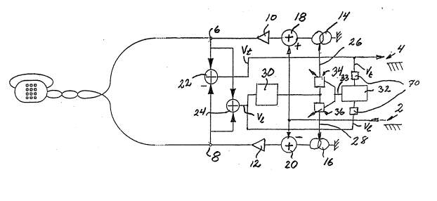
Fig. 1 shows an interface circuit of SLIC type between a four
wire line and a two wire line. It includes, on the one hand, a ;~
four wire interface with a receive input 2 and a send output 4, ;~
on the other hand, a two wire interface including two terminals 6
and 8 facing the two wire line, one for each wire. A raspective
output amplifier 10 and 12 and a respective current generator 14 `~
and 16 are connected to each terminal. -~
The circuit includes first circuit means, schematically
illustrated in the form of adders 18, 20, for applying via the `~
amplifiers 10 and 12 a signal received on the receive input 2 as
a differential signal on said terminals 6, 8 of the two wire
interface. Furthermore the circuit includes second circuit means,
schematically shown as a subtracting element 22, for feeding a
differential signal Vt received from the two wire line on said
terminals of the two wire interface 6, 8, to the send output 4.
Furthermore there are third circuit means, schematically ;~
"
3 2 ~
illustrated in the form of an adder ~4, for forming a
longitudinal signal Vl by means o~ the sum of voltages appearing
on each one of the terminals 6, 8. A respective feed back loop 26
and 28 for an adjusting signal extends via the respective current
generators 14 and 16 to each amplifier 10 and 12. This adjusting
signal is derived from the longitudinal signal Vl in a circuit 30
for adjusting the impedances 10, 18, 14 and 12, 20, 16,
respectively, of the two wire interface to earth, i.e. the so
called longitudinal terminating impedances. The adjustment signal
may be created in the circuit 30 in a way not described here in
detail, by comparing the longitudinal signal Vl with a
longitudinal reference.
That described thus far may be technique of the kind which is
e.g. kno~-n through the above mentioned Swedish patent 448,264 or
European patent 0,134,229, and also through the article "LINE
CIRCUIT COMPONENT SLIC FOR AXE 10" in Ericsson Review No. 4,
1983. Further description is therefore not re~uired here, since
details may be found in e.g. the publications just mentioned.
According to the invention there are furthermore correlator
and control circuits which are connected for receiving the ~ :
longitudinal signal Vl and a transversal signal Vt corresponding ~;~
the di~erential signal received from the two wire line on said
terminals of the two wire interface.
These correlator and control circuits include a correlator
circuit 32 realize~ to create a correction signal 33 baing a `~
measure of the correlation between the longitudinal signal Vl and
the transversal signal Vt. By means of this correction signal
there is performed an adaptive control in control circuits 34 and
36, respectively, of the amplifications in tha feed back loops so
as to minimize the correlation between Vl and Vt. More
particularly, the control circuits 34, 36 in the embodiment
according to Fig. 1, are realized to correct said adjustment
signal by means of the correction signal and located before each
one of the current generators 14 and 16, respectively. As regards
the detailed realization of such an adaptive system in general,
reference is made to the above mentioned document Adaptive Signal
Processing, Widrow & Stearns, ISBN 0-13-004029-0. Henceforth the
denomination "adaptive control loop" will be used for the control
loops extending from the elements 22, 24 via the correlator
--~ 213~321
7 ~-
circuit 32 and the respective control circuits 34 and 36, and
elements 14, 18, 10 and 16, 20, 12, respectively, back to the
elements 22, 24.
In Figs. 2-5, which show different embodiments, there are
included, for the sake o~ clearness, mainly only those circuit
parts which take care of the signal flow for obtaining adaptive
longitudinal balance in accordance with the invention. Circuit
parts taking care of the normal signal flow between the two wire
and four wire interfaces are thus not: shown. The longitudinal ;~
terminating impedances are represented only by blocks 40, and the `~
adjustment of these is illustrated by arrows 42 extending
directly from the correlator circuit 32 to these blocks 40.
. . ~ . ,.
The realization of the adaptive longitudinal balance may be -~-
made by means of digital or analogous signal treatment.
Fig. 2 shows a possible realization by means of digital . ;-~
signal treatment where the signals on the terminals 6 and 8 of
the two wire interface are fed, via an A/D converter 44 and 46, ~ `
respectively, to a digital signal treatment circuit 48 for cre~
ating Vt and Vl. A/D and D/A converters may, however, be located ~ ~
in other conceivable positions in the circuit. `;````
A modification of the solution in Fig. 2 is shown in Fig. 3. `~
The transversal signal in the receiving direction in the four
wire interface most often is digital. In a first separate
correlator part 50 it may suitably be correlated with the
longitudinal signal Vl from the two wire interface 6, 8. A
digital longitudinal received signal, if any, in the four wire
interface may in a corresponding way be correlated with a
transversal signal Vt from the two wire interface 6, 8 in a ~ ~
second separate correlator part 52. The advantage is that more ~ `
control of the incoming signals is obtained.
! ' In order to really use the adaptive longitudinal balancing in
accordance with the invention one may, with reference to Fig. 4,
let components with great spread of the component values, e.g.
over voltage protection elements 54, 56, 58, be included in the
adaptive control loop before the terminals 6, 8 of the two wire
interface.
In order to further increase the quality of the speech signal
one may, with reference to Fig. 5, combine the adaptive control
according to the invention with adaptive signal extinction. In ,,~ ~ `
- - . . ;`' '' ' :'.:
213~321
- ,. .
the Figure a variable filter is designated 60 to which the
longitudinal signal is fed for creating a negative copy thereof.
The negative copy is added to the transversal signal in an adder
62 the output signal of which is used for controlling the filter
60. Such adaptive signal extinction is a method used in many
connections but may not be used alone since it cannot cope with
the problem of cross-talk to nearby located two wire line pairs.
The latter is, however, dealt with by means of the adaptive
control according to the invention.
Here different embodiments o~ the blocks 32, 34 and 36 in
Fig. 1 will now be described more in detail. At first, however,
conceivable algorithms used in connection with creating the
correction signal in the correlator circuit 32 will be briefly
discussed.
When there is unbalance longitudinal signals will exist in
the transversal signal and vice versa. In other words, the
measured object is balanced if the transversal and longitudinal ~ `
signals are uncorrelated.
Two signals, such as Vt and Vl, although denominated x(t) and
y(t) in the discussion below, are uncorrelated at the times tl
and t2, respectively, if, and only if, the correlation
coefficient Rxy(tl,t2) is equal to zero, cf. Kristiansson,
Zetterberg - Signalteori, part 1, and
Rxy(tl,t2) = E( (X(tl)~mx(tl)*(y(t2)-my(t2)) ) (1) . ~.
sx(tl)*sy(t2)
where m in mx(t) and my(t) symbolizes that there is the question
of mean values of the signals, and s in sx(t~ and sy(t)
symbolizes that there is the question of the variance of the `
signalls . j ~,
Thus, a good error signal is thus the idle value of the
product of the two signals with the DC components filtered away.
In Fig. 1 filter circuits for filtering away the DC components
are indicated at 70.
If tl and t2 are equal and one tries to minimize the above
error signal it is only the resistive unbalance which is
compensated for. To be able to balance the capacitive or
inductive unbalance, i.e. the signals themselves are phase
213~321
g . .
shifted, one has to consider two cases. These will be f'ound by
means of a cross correlation matrix.
': '`' ~'
x(O)*y(O) x(l)*y(O) ..-- x(n)*y(O)
x(O)*y(l) x(l)*y(1) .... x(n)*y(1)
(2)
x(O)*y(n) x(l)*y(l) .... x~n)*y(n)
Either the contents y in x is minimized using the columns of
the matrix, or also the contents x in y using the rows of the i~
matrix. ~he "resistive'l correlation corresponds to the diagonal ~-
x(O)*y(O), x(l)*y(1) ... x(n)*y(n) in the matrix.
A sign algorithm for resistive balancing is obtained if one, `~
instead of performing multiplication in the correlation
measurement, compares the signs of the two signals in order to ~; ~
get hold of whether the correlation is positive or negative. ~ `
Updating of the variable quantities, i.e. in the present case ;~``
the change of the longitudinal balance, is performed in a fixed
step. Updating of the resistances is performed according to a
pattern which may be derived by means o~ a heuristic reasoning as -~
follows. `~
Fig. 6 illustrates a simulating model for the treatment of -~;
the longitudinal and transversal signals. Ra and Rb correspond to
the longitudinal input impedances together with R1. Rl has a
negative value in order to get the transversal impedance correct. "'''~"'f,'`~'''
Rm is a measuring resistance. In Ra and Rb errors are introduced
which shall be adapted away. It and Il, respectively, are
currents giving rise to unbalance voltages Vl and Vt, -~
respectively. ``~
In case of a longitudinal signal, i.e. It=O the error signal
is produced by forming sign(Vt(t)*VI(t)), i.e. the sign of the
product within brackets. If Ra is too big the amount of Va will ~- -
be greater than the amount of Vb, i.e. Vt is separated from zero. `~
In order to get balance, Ra shall be reduced and Rb increased. . ~
The opposite is true if Rb is too big. ~;
:.,- :,
'' ` "`'` '~' '
:,:
- 2~3~321
,.
The following table may be set up:
Vt ~I sign(Vt*VI) Ra Rb
neg. neg. pos. decrease increase
neg. pos. neg. increase decrease (3)
- pos. neg. neg. increase decrease
pOS. pO5. pOS. decrease increase
The same discussion may be used if a transversal signal is - ;~
put on, i.e. Il=O. This will give the same relation between
detected signs and correction.
The updating algorithm for Ra and Rb will thus be:
Ra(t)-Rb(t-to) - ~ * sign(Vt(t-to)*VI(t-to)) (4)
Rb(t)=Rb(t-to) + ~ * sign(Vt(t-to)*VI(t-to))
The positive constant ~ determines how fast the algorithm
converges and how big the remaining error is. ~;
~he advantage of the sign algorithm is that it is very ~`
simple.
A faster but somewhat more complex updating algorithm is
obtained if the multiplication is performed in the correlation ;-
measurement. Updating is otherwise done as in the sign algorithm.
The factor ~ should be conversely proportional to the power of
the siqnal, for the algorithm to be really effective. If both a
transversal and a longitudinal signal appears ~ has to be greatly ~ ;
decreased for having the algorithm to converge.
Ra(t)=Ra(t-to) - ~ * Vt(t-to)*VI(t-to) ~5)
Rb(t)=Rb(t-to) + ~ * Vt(t-to)*VI(t-to)
.
Fig. 7 shows an embodiment of the control circuits 34, 36
where they, in order to obtain a complex balancing, include
delays z-l with adjustable coefficients. By means of these delays
phase shifts may be created in the current response of the
impedances. More particularly, the control circuits 34 and 36 may
be so called FIR-filters (FIR=Finite Impulse Response). FIR-
filters are well known within the art of digital signal pro- -
cessing and are i.a. described in DIGITAL SIGNAL PROCESSING, by
~: '
~13~321 :
11 , ~ ,,
Alan V Oppenheim and Ronald W Schafer.
The coefficients k in the FIR filter may be adjusted and
describe the correlation between Vt and Vl in a way that depends
on the fact whether rows or columns are chosen in the cross
correlation matrix (1).
An embodiment of the correlator circuit 32 working according
to the sign algorithm (4) in the analogue version is shown in
Fig. 8. A comparator 72 receives the signals Vtand Vl provides an
output signal that follows the table (3), i.e. plus/minus a
consta~t voltage, and is fed to an integrator 74 on the output of
which the correction signal 33 appears, which is fed to the
control circuits 34 and 36.
In Fig. 9 there is shown an embodiment of the correlator
circuit 32 which uses the product of Vt and Vl, obtained from a ;`~;
multiplier 76. The product is integrated in an integrator 78
which at attainment of steady-state provides a constant output `
voltage. This voltage is a measure of the badness of the balance.
This corresponds to the above described proportional algorithm
(5). ``-"~
In Fig. 10 a further embodiment of the correlator circuit 32 ~ `~
is shown, in which the transversal signal is converted into
digital form by an A/D converter and is received by a circuit 80 ``
working with of a digital sign algorithm. . More particularly, ' -
this algorithm states that the correction at the time t is equal
to the correction at the time (t-1) + ~*sign(VI)*sign(Vt). The
signal created by this digital sign algorithm results in the
correction signal 33 after conversion in a D/A converter. Since ~ ~
the system is time discrete, problems arise with respect to ~ ;
folding distortion implying that Vt and Vl must be band limited. :
The analogous proposals do not have these problems. ;-;
, ~` ~`, ' `''';
' " ~ :. '